ICGOO在线商城 > 集成电路(IC) > PMIC - 稳压器 - DC DC 开关稳压器 > LM2575TV-5G
 Datasheet下载
- 型号: LM2575TV-5G
- 制造商: ON Semiconductor
- 库位|库存: xxxx|xxxx
- 要求:
| 数量阶梯 | 香港交货 | 国内含税 |
| +xxxx | $xxxx | ¥xxxx |
查看当月历史价格
查看今年历史价格
LM2575TV-5G产品简介:
ICGOO电子元器件商城为您提供LM2575TV-5G由ON Semiconductor设计生产,在icgoo商城现货销售,并且可以通过原厂、代理商等渠道进行代购。 LM2575TV-5G价格参考¥6.70-¥15.27。ON SemiconductorLM2575TV-5G封装/规格:PMIC - 稳压器 - DC DC 开关稳压器, 固定 降压,升压,降压升压 开关稳压器 IC 正或负 5V 1 输出 1A TO-220-5 成形引线。您可以下载LM2575TV-5G参考资料、Datasheet数据手册功能说明书,资料中有LM2575TV-5G 详细功能的应用电路图电压和使用方法及教程。
LM2575TV-5G 是一款由 ON Semiconductor(安森美半导体)生产的 DC-DC 开关稳压器,属于 PMIC(电源管理集成电路)类别。该型号为固定输出电压 5V 的降压型稳压器,广泛应用于需要高效、稳定直流电源转换的场景。以下是其主要应用场景:

1. 嵌入式系统
   LM2575TV-5G 常用于嵌入式系统的电源设计中,例如单片机(MCU)、微控制器或 DSP 的供电。它能够将较高的输入电压(如 12V 或 24V)转换为稳定的 5V 输出,满足大多数数字电路的需求。

2. 消费电子设备
   在消费电子产品中,如 USB 充电器、便携式音频设备、数码相机等,LM2575TV-5G 可以提供高效的电源转换,确保设备在不同输入电压条件下正常工作。

3. 工业控制
   工业自动化设备中,如 PLC(可编程逻辑控制器)、传感器接口模块和数据采集系统,需要稳定的 5V 电源来驱动逻辑电路和接口芯片。LM2575TV-5G 的高可靠性使其成为理想选择。

4. 通信设备
   在通信领域,如路由器、交换机和无线模块中,这款稳压器可以为通信芯片和接口电路提供稳定的电源支持,同时具备良好的电磁兼容性(EMC)性能。

5. 汽车电子
   虽然 LM2575TV-5G 不是专门针对汽车级应用设计,但在一些非关键车载设备中(如车用音响、导航仪或辅助控制单元),它可以用来将汽车电池电压转换为稳定的 5V 输出。

6. 实验与开发
   在实验室或开发阶段,工程师常使用 LM2575TV-5G 来快速搭建电源电路。其简单的设计和外部元件少的特点使得原型开发更加便捷。

 特点总结:
- 固定输出电压:5V
- 输入电压范围宽(7V 至 40V)
- 高效率开关稳压器(典型效率可达 80% 以上)
- 内置功率开关管,无需额外 MOSFET
- 外围电路简单,成本低

综上所述,LM2575TV-5G 适用于各种需要从较高电压转换为稳定 5V 输出的应用场合,特别是在对成本敏感且对性能要求适中的场景中表现尤为突出。
| 参数 | 数值 |
| 产品目录 | 集成电路 (IC)半导体 |
| 描述 | IC REG BUCK 5V 1A TO220-5稳压器—开关式稳压器 5V 1A PWR SW REG |
| 产品分类 | |
| 品牌 | ON Semiconductor |
| 产品手册 | |
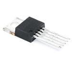
| 产品图片 |
|
| rohs | 符合RoHS无铅 / 符合限制有害物质指令(RoHS)规范要求 |
| 产品系列 | 电源管理 IC,稳压器—开关式稳压器,ON Semiconductor LM2575TV-5G- |
| 数据手册 | |
| 产品型号 | LM2575TV-5G |
| PWM类型 | 电压模式 |
| 产品种类 | 稳压器—开关式稳压器 |
| 供应商器件封装 | TO-220-5 |
| 其它名称 | LM2575TV-5G-ND |
| 包装 | 管件 |
| 同步整流器 | 无 |
| 商标 | ON Semiconductor |
| 安装类型 | 通孔 |
| 安装风格 | Through Hole |
| 封装/外壳 | TO-220-5 成形引线 |
| 封装/箱体 | TO-220-5 |
| 工作温度 | -40°C ~ 125°C |
| 工厂包装数量 | 50 |
| 开关频率 | 52 kHz |
| 最大输入电压 | 45 V |
| 标准包装 | 50 |
| 电压-输入 | 4.75 V ~ 40 V |
| 电压-输出 | 5V |
| 电流-输出 | 1A |
| 类型 | 降压(降压) |
| 系列 | LM2575 |
| 输出数 | 1 |
| 输出电压 | 5 V |
| 输出电流 | 1 A |
| 输出类型 | 固定 |
| 频率-开关 | 52kHz |


- 商务部:美国ITC正式对集成电路等产品启动337调查
- 曝三星4nm工艺存在良率问题 高通将骁龙8 Gen1或转产台积电
- 太阳诱电将投资9.5亿元在常州建新厂生产MLCC 预计2023年完工
- 英特尔发布欧洲新工厂建设计划 深化IDM 2.0 战略
- 台积电先进制程称霸业界 有大客户加持明年业绩稳了
- 达到5530亿美元!SIA预计今年全球半导体销售额将创下新高
- 英特尔拟将自动驾驶子公司Mobileye上市 估值或超500亿美元
- 三星加码芯片和SET,合并消费电子和移动部门,撤换高东真等 CEO
- 三星电子宣布重大人事变动 还合并消费电子和移动部门
- 海关总署:前11个月进口集成电路产品价值2.52万亿元 增长14.8%


PDF Datasheet 数据手册内容提取
LM2575, NCV2575 1.0 A, Adjustable Output Voltage, Step-Down Switching Regulator The LM2575 series of regulators are monolithic integrated circuits ideally suited for easy and convenient design of a step−down switching regulator (buck converter). All circuits of this series are http://onsemi.com capable of driving a 1.0 A load with excellent line and load regulation. These devices are available in fixed output voltages of 3.3 V, 5.0 V, 12 V, 15 V, and an adjustable output version. TO−220 These regulators were designed to minimize the number of external TV SUFFIX 1 components to simplify the power supply design. Standard series of CASE 314B inductors optimized for use with the LM2575 are offered by several 5 different inductor manufacturers. Since the LM2575 converter is a switch−mode power supply, its Heatsink surface connected to Pin 3 efficiency is significantly higher in comparison with popular three−terminal linear regulators, especially with higher input voltages. In many cases, the power dissipated by the LM2575 regulator is so low, that no heatsink is required or its size could be reduced dramatically. The LM2575 features include a guaranteed ±4% tolerance on output TO−220 voltage within specified input voltages and output load conditions, and T SUFFIX ±10% on the oscillator frequency (±2% over 0°C to 125°C). External CASE 314D 1 shutdown is included, featuring 80 (cid:2)A typical standby current. The output switch includes cycle−by−cycle current limiting, as well as 5 thermal shutdown for full protection under fault conditions. Pin 1. Vin 2. Output Features 3. Ground • 3.3 V, 5.0 V, 12 V, 15 V, and Adjustable Output Versions 4. Feedback • Adjustable Version Output Voltage Range of 1.23 V to 37 V ±4% 5. ON/OFF Maximum Over Line and Load Conditions • Guaranteed 1.0 A Output Current • Wide Input Voltage Range: 4.75 V to 40 V • D2PAK Requires Only 4 External Components • D2T SUFFIX 52 kHz Fixed Frequency Internal Oscillator 1 CASE 936A • TTL Shutdown Capability, Low Power Standby Mode 5 • High Efficiency • Heatsink surface (shown as terminal 6 in Uses Readily Available Standard Inductors case outline drawing) is connected to Pin 3 • Thermal Shutdown and Current Limit Protection • Moisture Sensitivity Level (MSL) Equals 1 • Pb−Free Packages are Available* ORDERING INFORMATION See detailed ordering and shipping information in the package Applications dimensions section on page 25 of this data sheet. • Simple and High−Efficiency Step−Down (Buck) Regulators • Efficient Pre−Regulator for Linear Regulators DEVICE MARKING INFORMATION • On−Card Switching Regulators See general marking information in the device marking • Positive to Negative Converters (Buck−Boost) section on page 26 of this data sheet. • Negative Step−Up Converters • Power Supply for Battery Chargers *For additional information on our Pb−Free strategy and soldering details, please download the ON Semiconductor Soldering and Mounting Techniques Reference Manual, SOLDERRM/D. © Semiconductor Components Industries, LLC, 2009 1 Publication Order Number: June, 2009 − Rev. 11 LM2575/D
LM2575, NCV2575 Typical Application (Fixed Output Voltage Versions) Feedback U7.n0r eVg -u la4t0e dV +Vin LM2575 4 330L 1(cid:2)H DC Input 1 Output 5.0 V Regulated 100 C(cid:2)Fin 3 GND 5 ON/OF2F D1N15819 Cout Output 1.0 A Load 330 (cid:2)F Representative Block Diagram and Typical Application Unregulated DC Input +Vin 3.1 V Internal ON/OFF ON/OFF Output R2 1 Regulator 5 Voltage Versions ((cid:3)) Cin 3.3 V 1.7 k 5.0 V 3.1 k 4 12 V 8.84 k Feedback 15 V 11.3 k Current R2 Fixed Gain Limit For adjustable version Error Amplifier Comparator R1 = open, R2 = 0 (cid:3) Driver Regulated R1 1.0 k Freq Latch L1 Output Shift Output Vout 18 kHz 1.0 Amp 2 1.235 V Switch GND D1 Cout Band-Gap 52 kHz Thermal Reference Oscillator Reset Shutdown 3 Load This device contains 162 active transistors. Figure 1. Block Diagram and Typical Application ABSOLUTE MAXIMUM RATINGS (Absolute Maximum Ratings indicate limits beyond which damage to the device may occur.) Rating Symbol Value Unit Maximum Supply Voltage Vin 45 V ON/OFF Pin Input Voltage − −0.3 V ≤ V ≤ +Vin V Output Voltage to Ground (Steady−State) − −1.0 V Power Dissipation Case 314B and 314D (TO−220, 5−Lead) PD Internally Limited W Thermal Resistance, Junction−to−Ambient R(cid:4)JA 65 °C/W Thermal Resistance, Junction−to−Case R(cid:4)JC 5.0 °C/W Case 936A (D2PAK) PD Internally Limited W Thermal Resistance, Junction−to−Ambient (Figure 34) R(cid:4)JA 70 °C/W Thermal Resistance, Junction−to−Case R(cid:4)JC 5.0 °C/W Storage Temperature Range Tstg −65 to +150 °C Minimum ESD Rating (Human Body Model: C = 100 pF, R = 1.5 k(cid:3)) − 2.0 kV Lead Temperature (Soldering, 10 s) − 260 °C Maximum Junction Temperature TJ 150 °C Stresses exceeding Maximum Ratings may damage the device. Maximum Ratings are stress ratings only. Functional operation above the Recommended Operating Conditions is not implied. Extended exposure to stresses above the Recommended Operating Conditions may affect device reliability. http://onsemi.com 2
LM2575, NCV2575 OPERATING RATINGS (Operating Ratings indicate conditions for which the device is intended to be functional, but do not guarantee specific performance limits. For guaranteed specifications and test conditions, see the Electrical Characteristics.) Rating Symbol Value Unit Operating Junction Temperature Range TJ −40 to +125 °C Supply Voltage Vin 40 V SYSTEM PARAMETERS ([Note 1] Test Circuit Figure 14) ELECTRICAL CHARACTERISTICS (Unless otherwise specified, Vin = 12 V for the 3.3 V, 5.0 V, and Adjustable version, Vin = 25 V for the 12 V version, and Vin = 30 V for the 15 V version. ILoad = 200 mA. For typical values TJ = 25°C, for min/max values TJ is the operating junction temperature range that applies [Note 2], unless otherwise noted.) Characteristics Symbol Min Typ Max Unit LM2575−3.3 (Note 1 Test Circuit Figure 14) Output Voltage (Vin = 12 V, ILoad = 0.2 A, TJ = 25°C) Vout 3.234 3.3 3.366 V Output Voltage (4.75 V ≤ Vin ≤ 40 V, 0.2 A ≤ ILoad ≤ 1.0 A) Vout V TJ = 25°C 3.168 3.3 3.432 TJ = −40 to +125°C 3.135 − 3.465 Efficiency (Vin = 12 V, ILoad = 1.0 A) η − 75 − % LM2575−5 ([Note 1] Test Circuit Figure 14) Output Voltage (Vin = 12 V, ILoad = 0.2 A, TJ = 25°C) Vout 4.9 5.0 5.1 V Output Voltage (8.0 V ≤ Vin ≤ 40 V, 0.2 A ≤ ILoad ≤ 1.0 A) Vout V TJ = 25°C 4.8 5.0 5.2 TJ = −40 to +125°C 4.75 − 5.25 Efficiency (Vin = 12 V, ILoad = 1.0 A) η − 77 − % LM2575−12 (Note 1 Test Circuit Figure 14) Output Voltage (Vin = 25 V, ILoad = 0.2 A, TJ = 25°C) Vout 11.76 12 12.24 V Output Voltage (15 V ≤ Vin ≤ 40 V, 0.2 A ≤ ILoad ≤ 1.0 A) Vout V TJ = 25°C 11.52 12 12.48 TJ = −40 to +125°C 11.4 − 12.6 Efficiency (Vin = 15V, ILoad = 1.0 A) η − 88 − % LM2575−15 (Note 1 Test Circuit Figure 14) Output Voltage (Vin = 30 V, ILoad = 0.2 A, TJ = 25°C) Vout 14.7 15 15.3 V Output Voltage (18 V ≤ Vin ≤ 40 V, 0.2 A ≤ ILoad ≤ 1.0 A) Vout V TJ = 25°C 14.4 15 15.6 TJ = −40 to +125°C 14.25 − 15.75 Efficiency (Vin = 18 V, ILoad = 1.0 A) η − 88 − % LM2575 ADJUSTABLE VERSION (Note 1 Test Circuit Figure 14) Feedback Voltage (Vin = 12 V, ILoad = 0.2 A, Vout = 5.0 V, TJ = 25°C) VFB 1.217 1.23 1.243 V Feedback Voltage (8.0 V ≤ Vin ≤ 40 V, 0.2 A ≤ ILoad ≤ 1.0 A, Vout = 5.0 V) VFB V TJ = 25°C 1.193 1.23 1.267 TJ = −40 to +125°C 1.18 − 1.28 Efficiency (Vin = 12 V, ILoad = 1.0 A, Vout = 5.0 V) η − 77 − % 1. External components such as the catch diode, inductor, input and output capacitors can affect switching regulator system performance. When the LM2575 is used as shown in the Figure 14 test circuit, system performance will be as shown in system parameters section. 2. Tested junction temperature range for the LM2575 and the NCV2575: Tlow = −40°C Thigh = +125°C http://onsemi.com 3
LM2575, NCV2575 DEVICE PARAMETERS ELECTRICAL CHARACTERISTICS (Unless otherwise specified, Vin = 12 V for the 3.3 V, 5.0 V, and Adjustable version, Vin = 25 V for the 12 V version, and Vin = 30 V for the 15 V version. ILoad = 200 mA. For typical values TJ = 25°C, for min/max values TJ is the operating junction temperature range that applies [Note 2], unless otherwise noted.) Characteristics Symbol Min Typ Max Unit ALL OUTPUT VOLTAGE VERSIONS Feedback Bias Current (Vout = 5.0 V Adjustable Version Only) Ib nA TJ = 25°C − 25 100 TJ = −40 to +125°C − − 200 Oscillator Frequency Note 3 fosc kHz TJ = 25°C − 52 − TJ = 0 to +125°C 47 − 58 TJ = −40 to +125°C 42 − 63 Saturation Voltage (Iout = 1.0 A Note 4) Vsat V TJ = 25°C − 1.0 1.2 TJ = −40 to +125°C − − 1.3 Max Duty Cycle (“on”) Note 5 DC 94 98 − % Current Limit (Peak Current Notes 4 and 3) ICL A TJ = 25°C 1.7 2.3 3.0 TJ = −40 to +125°C 1.4 − 3.2 Output Leakage Current Notes 6 and 7, TJ = 25°C IL mA Output = 0 V − 0.8 2.0 Output = −1.0 V − 6.0 20 Quiescent Current Note 6 IQ mA TJ = 25°C − 5.0 9.0 TJ = −40 to +125°C − − 11 Standby Quiescent Current (ON/OFF Pin = 5.0 V (“off”)) Istby (cid:2)A TJ = 25°C 15 80 200 TJ = −40 to +125°C − − 400 ON/OFF Pin Logic Input Level (Test Circuit Figure 14) V Vout = 0 V VIH TJ = 25°C 2.2 1.4 − TJ = −40 to +125°C 2.4 − − Vout = Nominal Output Voltage VIL TJ = 25°C − 1.2 1.0 TJ = −40 to +125°C − − 0.8 ON/OFF Pin Input Current (Test Circuit Figure 14) (cid:2)A ON/OFF Pin = 5.0 V (“off”), TJ = 25°C IIH − 15 30 ON/OFF Pin = 0 V (“on”), TJ = 25°C IIL − 0 5.0 3. The oscillator frequency reduces to approximately 18 kHz in the event of an output short or an overload which causes the regulated output voltage to drop approximately 40% from the nominal output voltage. This self protection feature lowers the average dissipation of the IC by lowering the minimum duty cycle from 5% down to approximately 2%. 4. Output (Pin 2) sourcing current. No diode, inductor or capacitor connected to output pin. 5. Feedback (Pin 4) removed from output and connected to 0 V. 6. Feedback (Pin 4) removed from output and connected to +12 V for the Adjustable, 3.3 V, and 5.0 V versions, and +25 V for the 12 V and 15 V versions, to force the output transistor “off”. 7. Vin = 40 V. http://onsemi.com 4
LM2575, NCV2575 TYPICAL PERFORMANCE CHARACTERISTICS (Circuit of Figure 14) 0.6 1.0 %) Vin = 20 V %) ILoad = 200 mA GE ( 0.4 INLooarmd =a li2z0e0d matA GE ( 0.8 TJ = 25°C HAN TJ = 25°C HAN C 0.2 C 0.6 3.3 V, 5.0 V and Adj E E G G A A LT 0 LT 0.4 O O V V T T U -0.2 U 0.2 P P T T U U O O , ut-0.4 , ut 0 12 V and 15 V Vo Vo -0.6 -0.2 -50 -25 0 25 50 75 100 125 0 5.0 10 15 20 25 30 35 40 TJ, JUNCTION TEMPERATURE (°C) Vin, INPUT VOLTAGE (V) Figure 2. Normalized Output Voltage Figure 3. Line Regulation 1.2 3.0 E (V) 1.1 A) 2.5 AG 1.0 T ( OLT 0.9 REN 2.0 N V -40°C UR O 0.8 C 1.5 TI T URA 0.7 25°C TPU T U 1.0 A O V, Ssat 00..56 125°C I, O 0.5 Vin = 25 V 0.4 0 0 0.1 0.2 0.3 0.4 0.5 0.6 0.7 0.8 0.9 1.0 -50 -25 0 25 50 75 100 125 SWITCH CURRENT (A) TJ, JUNCTION TEMPERATURE (°C) Figure 4. Switch Saturation Voltage Figure 5. Current Limit 2.0 20 V) (cid:5)Vout = 5% Vout = 5.0 V RENTIAL ( 11..86 ILoad = 1.0 A Rind = 0.2 (cid:3) RENT (mA) 1186 MGTJre o=au s2nu5dr°e PCdi nat T DIFFE 11..24 NT CUR 1142 ILoad = 1.0 A U E T-OUTP 01..80 ILoad = 200 mA QUIESC 81.00 ILoad = 200 mA PU , Q IN 0.6 I 6.0 0.4 4.0 -50 -25 0 25 50 75 100 125 0 5.0 10 15 20 25 30 35 40 TJ, JUNCTION TEMPERATURE (°C) Vin, INPUT VOLTAGE (V) Figure 6. Dropout Voltage Figure 7. Quiescent Current http://onsemi.com 5
LM2575, NCV2575 120 120 μNT ( (cid:2)A) 100 TJ = 25°C μNT ( (cid:2)A) 100 VViOn N=/O 1F2F V= 5.0 V E E R R R R U 80 U 80 C C T T N N CE 60 CE 60 S S E E UI UI Q 40 Q 40 Y Y B B D D AN 20 AN 20 T T S S , by 0 , by 0 Ist 0 5.0 10 15 20 25 30 35 40 Ist -50 -25 0 25 50 75 100 125 Vin, INPUT VOLTAGE (V) TJ, JUNCTION TEMPERATURE (°C) Figure 8. Standby Quiescent Current Figure 9. Standby Quiescent Current 2.0 40 Adjustable Y (%) 0 VNionr =m 1a2liz Ved at 25°C T (nA) Version Only C N 20 N E UE -2.0 RR Q U E C R N ZED F -4.0 CK PI 0 RMALI -6.0 EEDBA -20 O F N -8.0 , B F I -10 -40 -50 -25 0 25 50 75 100 125 -50 -25 0 25 50 75 100 125 TJ, JUNCTION TEMPERATURE (°C) TJ, JUNCTION TEMPERATURE (°C) Figure 10. Oscillator Frequency Figure 11. Feedback Pin Current E G OLTAmV) OUTPUT 10 V T VGE (100 VOLTAGE UN (PIN 2) 0 OUTPCHA 0 OUTPUT 1.0 A , ut -100 CURRENT Vo (PIN 2) 0 A) 1.0 A NT ( 1.0 INDUCTOR E CURRENT 0.5 A RR 0.5 U C OUTPUT 20 mV AD 0 RIPPLE /DIV LO VOLTAGE , d a o 5.0 (cid:2)s/DIV IL 100 (cid:2)s/DIV Figure 12. Switching Waveforms Figure 13. Load Transient Response http://onsemi.com 6
LM2575, NCV2575 5.0 Output Voltage Versions Feedback 4 Vin L1 Vout + 1 LM2575−5 330 (cid:2)H Regulated Output Output 2 Vin 3 GND 5 ON/OFF Unregulated Cin Cout DC Input 100 (cid:2)F/50 V D1 330 (cid:2)F 8.0 V - 40 V 1N5819 /16 V Load - Adjustable Output Voltage Versions Feedback 4 Vin LM2575 L1 Vout + 1 Adjustable 330 (cid:2)H Regulated Output Output 2 3 GND 5 ON/OFF UnDrCeg Iunlpautetd C10in0 (cid:2)F/50 V D1 C33o0ut (cid:2)F R2 8.0 V - 40 V Load 1N5819 /16 V R1 - (cid:3) (cid:5) V (cid:2)V 1(cid:4)(cid:2)R2 out ref(cid:2) R1 (cid:3) (cid:5) V R2(cid:2)R1 out(cid:2)(cid:2)1 V ref Where Vref = 1.23 V, R1 between 1.0 k(cid:3) and 5.0 k(cid:3) Figure 14. Typical Test Circuit PCB LAYOUT GUIDELINES As in any switching regulator, the layout of the printed On the other hand, the PCB area connected to the Pin 2 circuit board is very important. Rapidly switching currents (emitter of the internal switch) of the LM2575 should be associated with wiring inductance, stray capacitance and kept to a minimum in order to minimize coupling to sensitive parasitic inductance of the printed circuit board traces can circuitry. generate voltage transients which can generate Another sensitive part of the circuit is the feedback. It is electromagnetic interferences (EMI) and affect the desired important to keep the sensitive feedback wiring short. To operation. As indicated in the Figure 14, to minimize assure this, physically locate the programming resistors near inductance and ground loops, the length of the leads to the regulator, when using the adjustable version of the indicated by heavy lines should be kept as short as possible. LM2575 regulator. For best results, single−point grounding (as indicated) or ground plane construction should be used. http://onsemi.com 7
LM2575, NCV2575 PIN FUNCTION DESCRIPTION Pin Symbol Description (Refer to Figure 1) 1 Vin This pin is the positive input supply for the LM2575 step−down switching regulator. In order to minimize voltage transients and to supply the switching currents needed by the regulator, a suitable input bypass capacitor must be present (Cin in Figure 1). 2 Output This is the emitter of the internal switch. The saturation voltage Vsat of this output switch is typically 1.0 V. It should be kept in mind that the PCB area connected to this pin should be kept to a minimum in order to minimize coupling to sensitive circuitry. 3 GND Circuit ground pin. See the information about the printed circuit board layout. 4 Feedback This pin senses regulated output voltage to complete the feedback loop. The signal is divided by the internal resistor divider network R2, R1 and applied to the non−inverting input of the internal error amplifier. In the Adjustable version of the LM2575 switching regulator this pin is the direct input of the error amplifier and the resistor network R2, R1 is connected externally to allow programming of the output voltage. 5 ON/OFF It allows the switching regulator circuit to be shut down using logic level signals, thus dropping the total input supply current to approximately 80 (cid:2)A. The input threshold voltage is typically 1.4 V. Applying a voltage above this value (up to +Vin) shuts the regulator off. If the voltage applied to this pin is lower than 1.4 V or if this pin is connected to ground, the regulator will be in the “on” condition. DESIGN PROCEDURE Buck Converter Basics current loop. This removes the stored energy from the The LM2575 is a “Buck” or Step−Down Converter which inductor. is the most elementary forward−mode converter. Its basic The inductor current during this time is: schematic can be seen in Figure 15. (cid:3) (cid:5) The operation of this regulator topology has two distinct V V t out D off time periods. The first one occurs when the series switch is I (cid:2) on, the input voltage is connected to the input of the inductor. L(off) L The output of the inductor is the output voltage, and the This period ends when the power switch is once again rectifier (or catch diode) is reverse biased. During this turned on. Regulation of the converter is accomplished by period, since there is a constant voltage source connected varying the duty cycle of the power switch. It is possible to across the inductor, the inductor current begins to linearly describe the duty cycle as follows: ramp upwards, as described by the following equation: (cid:3) (cid:5) d(cid:2)ton, where T is the period of switching. T Vin Vout ton I (cid:2) For the buck converter with ideal components, the duty L(on) L cycle can also be described as: During this “on” period, energy is stored within the core V material in the form of magnetic flux. If the inductor is d(cid:2) out V properly designed, there is sufficient energy stored to carry in the requirements of the load during the “off” period. Figure 16 shows the buck converter idealized waveforms of the catch diode voltage and the inductor current. Power L Switch Vout Vin D1 Cout RLoad Figure 15. Basic Buck Converter The next period is the “off” period of the power switch. When the power switch turns off, the voltage across the inductor reverses its polarity and is clamped at one diode voltage drop below ground by catch dioded. Current now flows through the catch diode thus maintaining the load http://onsemi.com 8
LM2575, NCV2575 Von(SW) ge Power Power Power a olt Switch Switch Switch e V Off Power Off On od Switch Di On Time VD(FWD) nt e urr Ipk C or ILoad(AV) duct Imin Power Power In Diode Switch Diode Switch Time Figure 16. Buck Converter Idealized Waveforms http://onsemi.com 9
LM2575, NCV2575 Procedure (Fixed Output Voltage Version) In order to simplify the switching regulator design, a step−by−step design procedure and example is provided. Procedure Example Given Parameters: Given Parameters: Vout = Regulated Output Voltage (3.3 V, 5.0 V, 12 V or 15 V) Vout = 5.0 V Vin(max) = Maximum DC Input Voltage Vin(max) = 20 V ILoad(max) = Maximum Load Current ILoad(max) = 0.8 A 1. Controller IC Selection 1. Controller IC Selection According to the required input voltage, output voltage and According to the required input voltage, output voltage, current, select the appropriate type of the controller IC output current polarity and current value, use the LM2575−5 voltage version. controller IC 2. Input Capacitor Selection (Cin) 2. Input Capacitor Selection (Cin) To prevent large voltage transients from appearing at the input A 47 (cid:2)F, 25 V aluminium electrolytic capacitor located near and for stable operation of the converter, an aluminium or to the input and ground pins provides sufficient bypassing. tantalum electrolytic bypass capacitor is needed between the input pin +Vin and ground pin GND. This capacitor should be located close to the IC using short leads. This capacitor should have a low ESR (Equivalent Series Resistance) value. 3. Catch Diode Selection (D1) 3. Catch Diode Selection (D1) A.For this example the current rating of the diode is 1.0 A. A.Since the diode maximum peak current exceeds the regulator maximum load current the catch diode current rating must be at least 1.2 times greater than the maximum load current. For a robust design the diode should have a current rating equal to the maximum current limit of the LM2575 to be able to withstand a continuous output short B.Use a 30 V 1N5818 Schottky diode, or any of the B.The reverse voltage rating of the diode should be at least suggested fast recovery diodes shown in the Table 4. 1.25 times the maximum input voltage. 4. Inductor Selection (L1) 4. Inductor Selection (L1) A.According to the required working conditions, select the A.Use the inductor selection guide shown in Figures 17 correct inductor value using the selection guide from to 21. Figures 17 to 21. B.From the appropriate inductor selection guide, identify the B.From the selection guide, the inductance area intersected inductance region intersected by the Maximum Input by the 20 V line and 0.8 A line is L330. Voltage line and the Maximum Load Current line. Each region is identified by an inductance value and an inductor code. C.Select an appropriate inductor from the several different C.Inductor value required is 330 (cid:2)H. From the Table 1 or manufacturers part numbers listed in Table 1 or Table 2. Table 2, choose an inductor from any of the listed When using Table 2 for selecting the right inductor the manufacturers. designer must realize that the inductor current rating must be higher than the maximum peak current flowing through the inductor. This maximum peak current can be calculated as follows: (cid:3) (cid:5) I (cid:2)I (cid:4) VinVout ton p(max) Load(max) 2L where ton is the “on” time of the power switch and V out 1 ton (cid:2) Vin x fosc For additional information about the inductor, see the inductor section in the “External Components” section of this data sheet. http://onsemi.com 10
LM2575, NCV2575 Procedure (Fixed Output Voltage Version) (continued)In order to simplify the switching regulator design, a step−by−step design procedure and example is provided. Procedure Example 5. Output Capacitor Selection (Cout) 5. Output Capacitor Selection (Cout) A.Since the LM2575 is a forward−mode switching regulator A.Cout = 100 (cid:2)F to 470 (cid:2)F standard aluminium electrolytic. with voltage mode control, its open loop 2−pole−2−zero frequency characteristic has the dominant pole−pair determined by the output capacitor and inductor values. For stable operation and an acceptable ripple voltage, (approximately 1% of the output voltage) a value between 100 (cid:2)F and 470 (cid:2)F is recommended. B.Due to the fact that the higher voltage electrolytic capacitors B.Capacitor voltage rating = 16 V. generally have lower ESR (Equivalent Series Resistance) numbers, the output capacitor’s voltage rating should be at least 1.5 times greater than the output voltage. For a 5.0 V regulator, a rating at least 8V is appropriate, and a 10 V or 16 V rating is recommended. Procedure (Adjustable Output Version: LM2575−Adj) Procedure Example Given Parameters: Given Parameters: Vout = Regulated Output Voltage Vout = 8.0 V Vin(max) = Maximum DC Input Voltage Vin(max) = 12 V ILoad(max) = Maximum Load Current ILoad(max) = 1.0 A 1. Programming Output Voltage 1. Programming Output Voltage (selecting R1 and R2) To select the right programming resistor R1 and R2 value (see Select R1 and R2: Figure 14) use the following formula: (cid:3) (cid:5) (cid:3) (cid:5) Vout(cid:2)1.23 1(cid:4) RR21 Select R1 = 1.8 k(cid:3) ResistoVro Rut1 (cid:2)canV rbeef b1et(cid:4)weeRRn21 1.0w kh earned V 5re.0f =k (cid:3)1..2 (3F oVr best R2(cid:2)R1(cid:3)VVout(cid:6)1(cid:5)(cid:2)1.8k(cid:3)18..203VV(cid:6)1(cid:5) ref temperature coefficient and stability with time, use 1% metal film resistors). (cid:3) (cid:5) R2 = 9.91 k(cid:3), choose a 9.88 k metal film resistor. V R2(cid:2)R1 out 1 V ref 2. Input Capacitor Selection (Cin) 2. Input Capacitor Selection (Cin) To prevent large voltage transients from appearing at the input A 100 (cid:2)F aluminium electrolytic capacitor located near the and for stable operation of the converter, an aluminium or input and ground pin provides sufficient bypassing. tantalum electrolytic bypass capacitor is needed between the input pin +Vin and ground pin GND This capacitor should be located close to the IC using short leads. This capacitor should have a low ESR (Equivalent Series Resistance) value. For additional information see input capacitor section in the “External Components” section of this data sheet. 3. Catch Diode Selection (D1) 3. Catch Diode Selection (D1) A.Since the diode maximum peak current exceeds the A.For this example, a 3.0 A current rating is adequate. regulator maximum load current the catch diode current rating must be at least 1.2 times greater than the maximum load current. For a robust design, the diode should have a current rating equal to the maximum current limit of the LM2575 to be able to withstand a continuous output short. B.The reverse voltage rating of the diode should be at least B.Use a 20 V 1N5820 or MBR320 Schottky diode or any 1.25 times the maximum input voltage. suggested fast recovery diode in the Table 4. http://onsemi.com 11
LM2575, NCV2575 Procedure (Adjustable Output Version: LM2575−Adj) (continued) Procedure Example 4. Inductor Selection (L1) 4. Inductor Selection (L1) A.Use the following formula to calculate the inductor Volt x A.Calculate E x T [V x (cid:2)s] constant: microsecond [V x (cid:2)s] constant: (cid:3) (cid:5) ExT(cid:2) V V Vout x 106 [Vx(cid:2)s] ExT(cid:2)(cid:3)12 8.0(cid:5)x 8.0 x 1000(cid:2)51[Vx(cid:2)s] in out Von F[Hz] 12 52 B.Match the calculated E x T value with the corresponding B.E x T = 51 [V x (cid:2)s] number on the vertical axis of the Inductor Value Selection Guide shown in Figure 21. This E x T constant is a measure of the energy handling capability of an inductor and is dependent upon the type of core, the core area, the number of turns, and the duty cycle. C.Next step is to identify the inductance region intersected by C.ILoad(max) = 1.0 A the E x T value and the maximum load current value on the Inductance Region = L220 horizontal axis shown in Figure 21. D.From the inductor code, identify the inductor value. Then D.Proper inductor value = 220 (cid:2)H select an appropriate inductor from the Table 1 or Table 2. Choose the inductor from the Table 1 or Table 2. The inductor chosen must be rated for a switching frequency of 52 kHz and for a current rating of 1.15 x IIoad. The inductor current rating can also be determined by calculating the inductor peak cur(cid:3)rent: (cid:5) Vin Vout ton I (cid:2)I (cid:4) p(max) Load(max) 2L where ton is the “on” time of the power switch and V ton (cid:2) Voinut x fo1sc For additional information about the inductor, see the inductor section in the “External Components” section of this data sheet. 5. Output Capacitor Selection (Cout) 5. Output Capacitor Selection (Cout) A.Since the LM2575 is a forward−mode switching regulator A. with voltage mode control, its open loop 2−pole−2−zero Cout (cid:7)7.785 8.12220 (cid:2) 53μF frequency characteristic has the dominant pole−pair determined by the output capacitor and inductor values. To achieve an acceptable ripple voltage, select Cout = 100 (cid:2)F electrolytic capacitor. For stable operation, the capacitor must satisfy the following requirement: V C (cid:7)7.785 in(max) [μF] out V xL[μH] out B.Capacitor values between 10 (cid:2)F and 2000 (cid:2)F will satisfy the loop requirements for stable operation. To achieve an acceptable output ripple voltage and transient response, the output capacitor may need to be several times larger than the above formula yields. C.Due to the fact that the higher voltage electrolytic capacitors generally have lower ESR (Equivalent Series Resistance) numbers, the output capacitor’s voltage rating should be at least 1.5 times greater than the output voltage. For a 5.0 V regulator, a rating of at least 8V is appropriate, and a 10 V or 16 V rating is recommended. http://onsemi.com 12
LM2575, NCV2575 INDUCTOR VALUE SELECTION GUIDE 60 60 H1000 40 H1500 V) 20 V) 25 TAGE ( 1150 L680 L470 TAGE ( 2105 H1000 L680 L L O 8.0 O T V L330 T V 12 L470 PU 7.0 PU M IN L220 M IN 10 L330 U 6.0 L150 U 9.0 M M XI XI L220 A A , Mn L100 , Mn 8.0 L150 Vi Vi 5.0 7.0 0.2 0.3 0.4 0.5 0.6 0.8 1.0 0.2 0.3 0.4 0.5 0.6 0.7 0.8 0.9 1.0 IL, MAXIMUM LOAD CURRENT (A) IL, MAXIMUM LOAD CURRENT (A) Figure 17. LM2575−3.3 Figure 18. LM2575−5.0 60 60 V) 40 H2200 H1500 V) 40 H2200 GE ( 30 H1000 GE ( 3350 H1500 TA 25 H680 TA H1000 L L T VO 20 H470 T VO 25 H680 H470 PU PU 22 N 18 N UM I 17 L680 UM I 20 AXIM 16 L470 L330 AXIM 19 L680 L470 L330 , Mn 15 L220 , Mn 18 L220 Vi Vi 14 17 0.2 0.3 0.4 0.5 0.6 0.7 0.8 0.9 1.0 0.2 0.3 0.4 0.5 0.6 0.7 0.8 0.9 1.0 IL, MAXIMUM LOAD CURRENT (A) IL, MAXIMUM LOAD CURRENT (A) Figure 19. LM2575−12 Figure 20. LM2575−15 200 150 H2200 H1500 s) 125 H1000 μV 100 H680 H470 E ( M 80 TI 70 GE 60 L680 A LT 50 L470 O V 40 L330 T, E L220 30 L150 L100 20 0.2 0.3 0.4 0.5 0.6 0.7 0.8 0.9 1.0 IL, MAXIMUM LOAD CURRENT (A) Figure 21. LM2575−Adj NOTE: This Inductor Value Selection Guide is applicable for continuous mode only. http://onsemi.com 13
LM2575, NCV2575 Table 1. Inductor Selection Guide Inductor Inductor Code Value Pulse Eng Renco AIE Tech 39 L100 100 (cid:2)H PE−92108 RL2444 415−0930 77 308 BV L150 150 (cid:2)H PE−53113 RL1954 415−0953 77 358 BV L220 220 (cid:2)H PE−52626 RL1953 415−0922 77 408 BV L330 330 (cid:2)H PE−52627 RL1952 415−0926 77 458 BV L470 470 (cid:2)H PE−53114 RL1951 415−0927 − L680 680 (cid:2)H PE−52629 RL1950 415−0928 77 508 BV H150 150 (cid:2)H PE−53115 RL2445 415−0936 77 368 BV H220 220 (cid:2)H PE−53116 RL2446 430−0636 77 410 BV H330 330 (cid:2)H PE−53117 RL2447 430−0635 77 460 BV H470 470 (cid:2)H PE−53118 RL1961 430−0634 − H680 680 (cid:2)H PE−53119 RL1960 415−0935 77 510 BV H1000 1000 (cid:2)H PE−53120 RL1959 415−0934 77 558 BV H1500 1500 (cid:2)H PE−53121 RL1958 415−0933 − H2200 2200 (cid:2)H PE−53122 RL2448 415−0945 77 610 BV Table 2. Inductor Selection Guide Inductance Current Schott Renco Pulse Engineering Coilcraft ((cid:2)H) (A) THT SMT THT SMT THT SMT SMT 0.32 67143940 67144310 RL−1284−68−43 RL1500−68 PE−53804 PE−53804−S DO1608−68 0.58 67143990 67144360 RL−5470−6 RL1500−68 PE−53812 PE−53812−S DO3308−683 68 0.99 67144070 67144450 RL−5471−5 RL1500−68 PE−53821 PE−53821−S DO3316−683 1.78 67144140 67144520 RL−5471−5 − PE−53830 PE−53830−S DO5022P−683 0.48 67143980 67144350 RL−5470−5 RL1500−100 PE−53811 PE−53811−S DO3308−104 100 0.82 67144060 67144440 RL−5471−4 RL1500−100 PE−53820 PE−53820−S DO3316−104 1.47 67144130 67144510 RL−5471−4 − PE−53829 PE−53829−S DO5022P−104 0.39 − 67144340 RL−5470−4 RL1500−150 PE−53810 PE−53810−S DO3308−154 150 0.66 67144050 67144430 RL−5471−3 RL1500−150 PE−53819 PE−53819−S DO3316−154 1.20 67144120 67144500 RL−5471−3 − PE−53828 PE−53828−S DO5022P−154 0.32 67143960 67144330 RL−5470−3 RL1500−220 PE−53809 PE−53809−S DO3308−224 220 0.55 67144040 67144420 RL−5471−2 RL1500−220 PE−53818 PE−53818−S DO3316−224 1.00 67144110 67144490 RL−5471−2 − PE−53827 PE−53827−S DO5022P−224 0.42 67144030 67144410 RL−5471−1 RL1500−330 PE−53817 PE−53817−S DO3316−334 330 0.80 67144100 67144480 RL−5471−1 − PE−53826 PE−53826−S DO5022P−334 NOTE: Table 1 and Table 2 of this Indicator Selection Guide shows some examples of different manufacturer products suitable for design with the LM2575. http://onsemi.com 14
LM2575, NCV2575 Table 3. Example of Several Inductor Manufacturers Phone/Fax Numbers Phone + 1−619−674−8100 Pulse Engineering Inc. Fax + 1−619−674−8262 Phone + 353 93 24 107 Pulse Engineering Inc. Europe Fax + 353 93 24 459 Phone + 1−516−645−5828 Renco Electronics Inc. Fax + 1−516−586−5562 Phone + 1−813−347−2181 AIE Magnetics Fax Phone + 1−708−322−2645 Coilcraft Inc. Fax + 1−708−639−1469 Phone + 44 1236 730 595 Coilcraft Inc., Europe Fax + 44 1236 730 627 Phone + 33 8425 2626 Tech 39 Fax + 33 8425 2610 Phone + 1−612−475−1173 Schott Corp. Fax + 1−612−475−1786 Table 4. Diode Selection Guide gives an overview about both surface−mount and through−hole diodes for an effective design. Device listed in bold are available from ON Semiconductor. Schottky Ultra−Fast Recovery 1.0 A 3.0 A 1.0 A 3.0 A VR SMT THT SMT THT SMT THT SMT THT 20 V SK12 1N5817 SK32 1N5820 SR102 MBRD320 MBR320 SR302 30 V MBRS130LT3 1N5818 SK33 1N5821 MURS320T3 SK13 SR103 MBRD330 MBR330 MURS120T3 MUR120 11DQ03 SR303 11DF1 31DQ03 HER102 40 V MBRS140T3 1N5819 MBRS340T3 1N5822 10BF10 MURD320 MUR320 SK14 SR104 MBRD340 MBR340 30WF10 10BQ040 11DQ04 30WQ04 SR304 MUR420 10MQ040 SK34 31DQ04 50 V MBRS150 MBR150 MBRD350 MBR350 31DF1 10BQ050 SR105 SK35 SR305 HER302 11DQ05 30WQ05 11DQ05 http://onsemi.com 15
LM2575, NCV2575 EXTERNAL COMPONENTS Input Capacitor (C ) (below 0.05 (cid:3)), there is a possibility of an unstable feedback in The Input Capacitor Should Have a Low ESR loop, resulting in oscillation at the output. This situation can For stable operation of the switch mode converter a low occur when a tantalum capacitor, that can have a very low ESR (Equivalent Series Resistance) aluminium or solid ESR, is used as the only output capacitor. tantalum bypass capacitor is needed between the input pin At Low Temperatures, Put in Parallel Aluminium and the ground pin to prevent large voltage transients from Electrolytic Capacitors with Tantalum Capacitors appearing at the input. It must be located near the regulator Electrolytic capacitors are not recommended for and use short leads. With most electrolytic capacitors, the temperatures below −25°C. The ESR rises dramatically at capacitance value decreases and the ESR increases with cold temperatures and typically rises 3 times at −25°C and lower temperatures. For reliable operation in temperatures below −25°C larger values of the input capacitor may be as much as 10 times at −40°C. Solid tantalum capacitors have much better ESR spec at cold temperatures and are needed. Also paralleling a ceramic or solid tantalum recommended for temperatures below −25°C. They can be capacitor will increase the regulator stability at cold also used in parallel with aluminium electrolytics. The value temperatures. of the tantalum capacitor should be about 10% or 20% of the RMS Current Rating of Cin total capacitance. The output capacitor should have at least The important parameter of the input capacitor is the RMS 50% higher RMS ripple current rating at 52 kHz than the current rating. Capacitors that are physically large and have peak−to−peak inductor ripple current. large surface area will typically have higher RMS current ratings. For a given capacitor value, a higher voltage Catch Diode electrolytic capacitor will be physically larger than a lower Locate the Catch Diode Close to the LM2575 voltage capacitor, and thus be able to dissipate more heat to The LM2575 is a step−down buck converter; it requires a the surrounding air, and therefore will have a higher RMS fast diode to provide a return path for the inductor current current rating. The consequence of operating an electrolytic when the switch turns off. This diode must be located close capacitor above the RMS current rating is a shortened to the LM2575 using short leads and short printed circuit operating life. In order to assure maximum capacitor traces to avoid EMI problems. operating lifetime, the capacitor’s RMS ripple current rating Use a Schottky or a Soft Switching should be: Ultra−Fast Recovery Diode Irms > 1.2 x d x ILoad Since the rectifier diodes are very significant source of losses within switching power supplies, choosing the where d is the duty cycle, for a buck regulator rectifier that best fits into the converter design is an d(cid:2)ton(cid:2)Vout important process. Schottky diodes provide the best T V performance because of their fast switching speed and low in and d(cid:2)toTn(cid:2)|V |V|o(cid:4)ut|V for abuck(cid:6)boost regulator. forTwhaeryd pvroolvtaidgee tdhreo bpe.st efficiency especially in low output out in voltage applications (5.0 V and lower). Another choice could be Fast−Recovery, or Ultra−Fast Recovery diodes. It Output Capacitor (C ) out has to be noted, that some types of these diodes with an For low output ripple voltage and good stability, low ESR abrupt turnoff characteristic may cause instability or EMI output capacitors are recommended. An output capacitor troubles. has two main functions: it filters the output and provides A fast−recovery diode with soft recovery characteristics regulator loop stability. The ESR of the output capacitor and can better fulfill a quality, low noise design requirements. the peak−to−peak value of the inductor ripple current are the Table 4 provides a list of suitable diodes for the LM2575 main factors contributing to the output ripple voltage value. regulator. Standard 50/60 Hz rectifier diodes such as the Standard aluminium electrolytics could be adequate for 1N4001 series or 1N5400 series are NOT suitable. some applications but for quality design low ESR types are recommended. Inductor An aluminium electrolytic capacitor’s ESR value is The magnetic components are the cornerstone of all related to many factors such as the capacitance value, the switching power supply designs. The style of the core and voltage rating, the physical size and the type of construction. the winding technique used in the magnetic component’s In most cases, the higher voltage electrolytic capacitors have design has a great influence on the reliability of the overall lower ESR value. Often capacitors with much higher power supply. voltage ratings may be needed to provide low ESR values Using an improper or poorly designed inductor can cause that are required for low output ripple voltage. high voltage spikes generated by the rate of transitions in current within the switching power supply, and the The Output Capacitor Requires an ESR Value possibility of core saturation can arise during an abnormal That Has an Upper and Lower Limit operational mode. Voltage spikes can cause the As mentioned above, a low ESR value is needed for low semiconductors to enter avalanche breakdown and the part output ripple voltage, typically 1% to 2% of the output can instantly fail if enough energy is applied. It can also voltage. But if the selected capacitor’s ESR is extremely low http://onsemi.com 16
LM2575, NCV2575 cause significant RFI (Radio Frequency Interference) and the physical volume the inductor must fit within, and the EMI (Electro−Magnetic Interference) problems. amount of EMI (Electro−Magnetic Interference) shielding that the core must provide. The inductor selection guide Continuous and Discontinuous Mode of Operation covers different styles of inductors, such as pot core, E−core, The LM2575 step−down converter can operate in both the toroid and bobbin core, as well as different core materials continuous and the discontinuous modes of operation. The such as ferrites and powdered iron from different regulator works in the continuous mode when loads are manufacturers. relatively heavy, the current flows through the inductor For high quality design regulators the toroid core seems to continuously and never falls to zero. Under light load be the best choice. Since the magnetic flux is completely conditions, the circuit will be forced to the discontinuous contained within the core, it generates less EMI, reducing mode when inductor current falls to zero for certain period noise problems in sensitive circuits. The least expensive is of time (see Figure 22 and Figure 23). Each mode has the bobbin core type, which consists of wire wound on a distinctively different operating characteristics, which can ferrite rod core. This type of inductor generates more EMI affect the regulator performance and requirements. In many due to the fact that its core is open, and the magnetic flux is cases the preferred mode of operation is the continuous not completely contained within the core. mode. It offers greater output power, lower peak currents in When multiple switching regulators are located on the the switch, inductor and diode, and can have a lower output same printed circuit board, open core magnetics can cause ripple voltage. On the other hand it does require larger interference between two or more of the regulator circuits, inductor values to keep the inductor current flowing especially at high currents due to mutual coupling. A toroid, continuously, especially at low output load currents and/or pot core or E−core (closed magnetic structure) should be high input voltages. used in such applications. To simplify the inductor selection process, an inductor selection guide for the LM2575 regulator was added to this Do Not Operate an Inductor Beyond its data sheet (Figures 17 through 21). This guide assumes that Maximum Rated Current the regulator is operating in the continuous mode, and Exceeding an inductor’s maximum current rating may selects an inductor that will allow a peak−to−peak inductor cause the inductor to overheat because of the copper wire ripple current to be a certain percentage of the maximum losses, or the core may saturate. Core saturation occurs when design load current. This percentage is allowed to change as the flux density is too high and consequently the cross different design load currents are selected. For light loads sectional area of the core can no longer support additional (less than approximately 200 mA) it may be desirable to lines of magnetic flux. operate the regulator in the discontinuous mode, because the This causes the permeability of the core to drop, the inductor value and size can be kept relatively low. inductance value decreases rapidly and the inductor begins Consequently, the percentage of inductor peak−to−peak to look mainly resistive. It has only the dc resistance of the current increases. This discontinuous mode of operation is winding. This can cause the switch current to rise very perfectly acceptable for this type of switching converter. rapidly and force the LM2575 internal switch into Any buck regulator will be forced to enter discontinuous cycle−by−cycle current limit, thus reducing the dc output mode if the load current is light enough. load current. This can also result in overheating of the inductor and/or the LM2575. Different inductor types have different saturation characteristics, and this should be kept H WITCT (A)1.0 in mind when selecting an inductor. SN R RE POWECUR 0 WITCHT (A)0.1 SN ORT (A)1.0 WER URRE 0 TN OC CE P UR DR NU IC 0 ORT (A)0.1 HORIZONTAL TIME BASE: 5.0 (cid:2)s/DIV CTEN UR DR 0 NU Figure 22. Continuous Mode Switching IC Current Waveforms HORIZONTAL TIME BASE: 5.0 (cid:2)s/DIV Selecting the Right Inductor Style Figure 23. Discontinuous Mode Switching Some important considerations when selecting a core type Current Waveforms are core material, cost, the output power of the power supply, http://onsemi.com 17
LM2575, NCV2575 GENERAL RECOMMENDATIONS Output Voltage Ripple and Transients Heatsinking and Thermal Considerations Source of the Output Ripple The Through−Hole Package TO−220 Since the LM2575 is a switch mode power supply The LM2575 is available in two packages, a 5−pin regulator, its output voltage, if left unfiltered, will contain a TO−220(T, TV) and a 5−pin surface mount D2PAK(D2T). sawtooth ripple voltage at the switching frequency. The There are many applications that require no heatsink to keep output ripple voltage value ranges from 0.5% to 3% of the the LM2575 junction temperature within the allowed output voltage. It is caused mainly by the inductor sawtooth operating range. The TO−220 package can be used without ripple current multiplied by the ESR of the output capacitor. a heatsink for ambient temperatures up to approximately 50°C (depending on the output voltage and load current). Short Voltage Spikes and How to Reduce Them Higher ambient temperatures require some heatsinking, The regulator output voltage may also contain short either to the printed circuit (PC) board or an external voltage spikes at the peaks of the sawtooth waveform (see heatsink. Figure 24). These voltage spikes are present because of the fast switching action of the output switch, and the parasitic The Surface Mount Package D2PAK and its inductance of the output filter capacitor. There are some Heatsinking other important factors such as wiring inductance, stray The other type of package, the surface mount D2PAK, is capacitance, as well as the scope probe used to evaluate these designed to be soldered to the copper on the PC board. The transients, all these contribute to the amplitude of these copper and the board are the heatsink for this package and spikes. To minimize these voltage spikes, low inductance the other heat producing components, such as the catch capacitors should be used, and their lead lengths must be diode and inductor. The PC board copper area that the kept short. The importance of quality printed circuit board package is soldered to should be at least 0.4 in2 (or 100 mm2) layout design should also be highlighted. and ideally should have 2 or more square inches (1300 mm2) of 0.0028 inch copper. Additional increasing of copper area Voltage spikes caused by switching action of the output beyond approximately 3.0 in2 (2000 mm2) will not improve switch and the parasitic inductance of the output capacitor heat dissipation significantly. If further thermal improvements are needed, double sided or multilayer PC boards with large copper areas should be considered. UNFILTERED OUTPUT Thermal Analysis and Design VOLTAGE The following procedure must be performed to determine whether or not a heatsink will be required. First determine: VERTICAL RESOLUTION: 1. P maximum regulator power dissipation in D(max) 20 mV/DIV the application. FILTERED 2. TA(max) maximum ambient temperature in the OUTPUT application. VOLTAGE 3. T maximum allowed junction temperature J(max) (125°C for the LM2575). For a conservative HORIZONTAL TIME BASE: 10 (cid:2)s/DIV design, the maximum junction temperature Figure 24. Output Ripple Voltage Waveforms should not exceed 110°C to assure safe operation. For every additional 10°C Minimizing the Output Ripple temperature rise that the junction must In order to minimize the output ripple voltage it is possible withstand, the estimated operating lifetime to enlarge the inductance value of the inductor L1 and/or to of the component is halved. use a larger value output capacitor. There is also another way 4. R(cid:4)JC package thermal resistance junction−case. to smooth the output by means of an additional LC filter (20 (cid:2)H, 100 (cid:2)F), that can be added to the output (see 5. R(cid:4)JA package thermal resistance junction−ambient. (Refer to Absolute Maximum Ratings in this data sheet or Figure 33) to further reduce the amount of output ripple and transients. With such a filter it is possible to reduce the R(cid:4)JC and R(cid:4)JA values). output ripple voltage transients 10 times or more. Figure 24 The following formula is to calculate the total power shows the difference between filtered and unfiltered output dissipated by the LM2575: waveforms of the regulator shown in Figure 33. P = (V x I ) + d x I x V D in Q Load sat The upper waveform is from the normal unfiltered output where d is the duty cycle and for buck converter of the converter, while the lower waveform shows the output ripple voltage filtered by an additional LC filter. http://onsemi.com 18
LM2575, NCV2575 d(cid:2)ton(cid:2)VO, UDCnr eIngpuulatted Feedback T Vin 12 V to 25 V +Vin 4 L1 LM2575−12 100 (cid:2)H IQ (quiescent current) and Vsat can be found in the Cin 1 Output LM2575 data sheet, 100 (cid:2)F 2 /50 V 3 GND 5 ON/OFF D1 Cout Vin is minimum input voltage applied, 1N5819 1800 (cid:2)F V is the regulator output voltage, /16 V O I is the load current. Load Regulated The dynamic switching losses during turn−on and Output -12 V @ 0.35 A turn−off can be neglected if proper type catch diode is used. Packages Not on a Heatsink (Free−Standing) Figure 25. Inverting Buck−Boost Regulator Using the For a free−standing application when no heatsink is used, LM2575−12 Develops −12 V @ 0.35 A the junction temperature can be determined by the following expression: ADDITIONAL APPLICATIONS TJ = (R(cid:4)JA) (PD) + TA Inverting Regulator An inverting buck−boost regulator using the LM2575−12 where (R(cid:4)JA)(PD) represents the junction temperature rise is shown in Figure 25. This circuit converts a positive input caused by the dissipated power and T is the maximum A voltage to a negative output voltage with a common ground ambient temperature. by bootstrapping the regulators ground to the negative Packages on a Heatsink output voltage. By grounding the feedback pin, the regulator If the actual operating junction temperature is greater than senses the inverted output voltage and regulates it. the selected safe operating junction temperature determined In this example the LM2575−12 is used to generate a in step 3, than a heatsink is required. The junction −12 V output. The maximum input voltage in this case temperature will be calculated as follows: cannot exceed +28 V because the maximum voltage appearing across the regulator is the absolute sum of the TJ = PD (R(cid:4)JA + R(cid:4)CS + R(cid:4)SA) + TA input and output voltages and this must be limited to a where R(cid:4)JC is the thermal resistance junction−case, maximum of 40 V. R(cid:4)CS is the thermal resistance case−heatsink, This circuit configuration is able to deliver approximately R(cid:4)SA is the thermal resistance heatsink−ambient. 0.35 A to the output when the input voltage is 12 V or higher. If the actual operating temperature is greater than the At lighter loads the minimum input voltage required drops selected safe operating junction temperature, then a larger to approximately 4.7 V, because the buck−boost regulator heatsink is required. topology can produce an output voltage that, in its absolute value, is either greater or less than the input voltage. Some Aspects That can Influence Thermal Design Since the switch currents in this buck−boost configuration It should be noted that the package thermal resistance and are higher than in the standard buck converter topology, the the junction temperature rise numbers are all approximate, available output current is lower. and there are many factors that will affect these numbers, This type of buck−boost inverting regulator can also such as PC board size, shape, thickness, physical position, require a larger amount of startup input current, even for location, board temperature, as well as whether the light loads. This may overload an input power source with surrounding air is moving or still. a current limit less than 1.5 A. Other factors are trace width, total printed circuit copper Such an amount of input startup current is needed for at area, copper thickness, single− or double−sided, multilayer least 2.0 ms or more. The actual time depends on the output board, the amount of solder on the board or even color of the voltage and size of the output capacitor. traces. Because of the relatively high startup currents required by The size, quantity and spacing of other components on this inverting regulator topology, the use of a delayed startup the board can also influence its effectiveness to dissipate or an undervoltage lockout circuit is recommended. the heat. http://onsemi.com 19
LM2575, NCV2575 Using a delayed startup arrangement, the input capacitor can charge up to a higher voltage before the switch−mode +Vin +Vin regulator begins to operate. LM2575−XX 1 The high input current needed for startup is now partially supplied by the input capacitor Cin. C10in0 (cid:2)F 47R 1k Shutdown 5 ON/OFF 3 GND Design Recommendations: Input 5.0 V The inverting regulator operates in a different manner Off than the buck converter and so a different design procedure 0 R3 has to be used to select the inductor L1 or the output On 470 R2 47 k capacitor C . out The output capacitor values must be larger than is -Vout normally required for buck converter designs. Low input MOC8101 voltages or high output currents require a large value output capacitor (in the range of thousands of (cid:2)F). NOTE: This picture does not show the complete circuit. The recommended range of inductor values for the inverting converter design is between 68 (cid:2)H and 220 (cid:2)H. To Figure 27. Inverting Buck−Boost Regulator Shut Down Circuit Using an Optocoupler select an inductor with an appropriate current rating, the inductor peak current has to be calculated. With the inverting configuration, the use of the ON/OFF The following formula is used to obtain the peak inductor pin requires some level shifting techniques. This is caused current: by the fact, that the ground pin of the converter IC is no I (cid:8) ILoad(Vin (cid:4) |VO|) (cid:4) Vinxton longer at ground. Now, the ON/OFF pin threshold voltage peak V 2L (1.4 V approximately) has to be related to the negative in 1 |V | output voltage level. There are many different possible shut whereton (cid:2) Vin (cid:4)O|VO| x fo1sc, and fosc (cid:2) 52kHz. down methods, two of them are shown in Figures 27 and 28. Under normal continuous inductor current operating +V Shutdown conditions, the worst case occurs when Vin is minimal. Off Input Note that the voltage appearing across the regulator is the 0 On absolute sum of the input and output voltage, and must not R2 5.6 k exceed 40 V. +Vin +Vin Unregulated 1 DC Input Feedback Cin LM2575−XX 12 V to 25 V +Vin 4 L1 100 (cid:2)F LM2575−12 100 (cid:2)H 100 C(cid:2)Fin C1 1 O2utput Q2N13906 5 ON/OFF 3 GND /50 V 0.1 (cid:2)F 5 ON/OFF3 GND D1 Cout R1 4R71 k R2 1N5819 1/1860 V0 (cid:2)F 12 k -Vout 47 k NOTE: This picture does not show the complete circuit. Regulated Figure 28. Inverting Buck−Boost Regulator Shut Down Output -12 V @ 0.35 A Circuit Using a PNP Transistor Figure 26. Inverting Buck−Boost Regulator with Delayed Startup Negative Boost Regulator This example is a variation of the buck−boost topology and is called a negative boost regulator. This regulator It has been already mentioned above, that in some experiences relatively high switch current, especially at low situations, the delayed startup or the undervoltage lockout input voltages. The internal switch current limiting results in features could be very useful. A delayed startup circuit lower output load current capability. applied to a buck−boost converter is shown in Figure 26. The circuit in Figure 29 shows the negative boost Figure 32 in the “Undervoltage Lockout” section describes configuration. The input voltage in this application ranges an undervoltage lockout feature for the same converter from −5.0 V to −12 V and provides a regulated −12 V output. topology. http://onsemi.com 20
LM2575, NCV2575 If the input voltage is greater than −12 V, the output will rise cause some problems by coupling the ripple into the above −12 V accordingly, but will not damage the regulator. ON/OFF pin, the regulator could be switched periodically on and off with the line (or double) frequency. 4 C10o0ut0 (cid:2)F +Vin +Vin LM2575−XX +Vin LM2575−12 Feedback /16 V 1 D1 1 Output C1 100 C(cid:2)Fin 3 GND 5 ON/O2FF 1N5817 ReOguutlpautetd Cin 0.1 (cid:2)F 5 ON/OFF 3 GND /50 V Vout = -12 V 100 (cid:2)F R1 47 k R2 Load Current from 47 k L1 200 mA for Vin = -5.2 V to 500 mA for Vin = -7.0 V 150 (cid:2)H Unregulated DC Input NOTE: This picture does not show the complete circuit. -Vin = -5.0 V to -12 V Figure 30. Delayed Startup Circuitry Figure 29. Negative Boost Regulator Undervoltage Lockout Design Recommendations: Some applications require the regulator to remain off until The same design rules as for the previous inverting the input voltage reaches a certain threshold level. Figure 31 buck−boost converter can be applied. The output capacitor shows an undervoltage lockout circuit applied to a buck Cout must be chosen larger than would be required for a regulator. A version of this circuit for buck−boost converter standard buck converter. Low input voltages or high output is shown in Figure 32. Resistor R3 pulls the ON/OFF pin currents require a large value output capacitor (in the range high and keeps the regulator off until the input voltage of thousands of (cid:2)F). The recommended range of inductor reaches a predetermined threshold level, which is values for the negative boost regulator is the same as for determined by the following expression: inverting converter design. (cid:3) (cid:5) Another important point is that these negative boost Vth(cid:8)VZ1(cid:4) 1(cid:4)RR21 VBE(Q1) converters cannot provide current limiting load protection in the event of a short in the output so some other means, such as a fuse, may be necessary to provide the load protection. +Vin +Vin Delayed Startup LM2575−5.0 1 There are some applications, like the inverting regulator already mentioned above, which require a higher amount of R2 R3 Cin startup current. In such cases, if the input power source is 10 k 47 k 100 (cid:2)F 5 ON/OFF 3 GND limited, this delayed startup feature becomes very useful. To provide a time delay between the time the input voltage Z1 is applied and the time when the output voltage comes up, 1N5242B the circuit in Figure 30 can be used. As the input voltage is Q1 applied, the capacitor C1 charges up, and the voltage across 2N3904 the resistor R2 falls down. When the voltage on the ON/OFF R1 Vth ≈ 13 V pin falls below the threshold value 1.4 V, the regulator starts 10 k up. Resistor R1 is included to limit the maximum voltage applied to the ON/OFF pin, reduces the power supply noise sensitivity, and also limits the capacitor C1 discharge NOTE: This picture does not show the complete circuit. current, but its use is not mandatory. Figure 31. Undervoltage Lockout Circuit for When a high 50 Hz or 60 Hz (100 Hz or 120 Hz Buck Converter respectively) ripple voltage exists, a long delay time can http://onsemi.com 21
LM2575, NCV2575 Adjustable Output, Low−Ripple Power Supply A 1.0 A output current capability power supply that +Vin +Vin features an adjustable output voltage is shown in Figure 33. LM2575−5.0 1 This regulator delivers 1.0 A into 1.2 V to 35 V output. The input voltage ranges from roughly 8.0 V to 40 V. In order R2 R3 Cin 15 k 68 k 100 (cid:2)F 5 ON/OFF 3 GND to achieve a 10 or more times reduction of output ripple, an additional L−C filter is included in this circuit. Z1 1N5242B Vth ≈ 13 V Q1 2N3904 R1 15 k Vout = -5.0 V NOTE: This picture does not show the complete circuit. Figure 32. Undervoltage Lockout Circuit for Buck−Boost Converter Feedback Unregulated 4 D+C Input +Vi1n LM2575−Adj 150L 1(cid:2)H 20L (cid:2)2H Regulated Output Output Voltage 2 1.2 V to 35 V @1.0 A 3 GND 5 ON/OFF R2 50 k C1 Cin 100 (cid:2)F 100 (cid:2)F D1 Cout /50 V 1N5819 2200 (cid:2)F R1 1.1 k Optional Output Ripple Filter Figure 33. Adjustable Power Supply with Low Ripple Voltage 80 PD(max) for TA = 50°C 3.5 N (W) E O ESISTANC°R ( C/W) 6700 VMFeroeruteinc atAelildry 2.0 oz. Copper 23..50 DISSIPATI HERMAL R TION‐TO‐AI 50 MSiizneim Puamd LÎÎÎÎÎÎL ÎÎÎÎÎÎ2.0 M POWER , TθJAJUNC 40 ÎÎÎÎ1.5 AXIMU R M R(cid:4)JA , D P 30 1.0 0 5.0 10 15 20 25 30 L, LENGTH OF COPPER (mm) Figure 34. D2PAK Thermal Resistance and Maximum Power Dissipation versus P.C.B. Copper Length http://onsemi.com 22
LM2575, NCV2575 THE LM2575−5.0 STEP−DOWN VOLTAGE REGULATOR WITH 5.0 V @ 1.0 A OUTPUT POWER CAPABILITY. TYPICAL APPLICATION WITH THROUGH−HOLE PC BOARD LAYOUT Feedback 4 Unregulated +Vin L1 +Vin = +7.0 V DtoC + I4n0p uVt 1 LM2575−5.0 Output 330 (cid:2)H Regulated Output 2 +Vout1 = 5.0 V @ 1.0 A 3 GND 5 ON/OFF C1 100 (cid:2)F J1 D1 Cout /50 V 1N5819 330 (cid:2)F /16 V GNDin GNDout C1 − 100 (cid:2)F, 50 V, Aluminium Electrolytic C2 − 330 (cid:2)F, 16 V, Aluminium Electrolytic D1 − 1.0 A, 40 V, Schottky Rectifier, 1N5819 L1 − 330 (cid:2)H, Tech 39: 77 458 BV, Toroid Core, Through−Hole, Pin 3 = Start, Pin 7 = Finish Figure 35. Schematic Diagram of the LM2575−5.0 Step−Down Converter GNDin U1 LM2575 GNDout C1 J1 C2 D1 L1 DC-DC Converter +Vin +Vout1 NOTE: Not to scale. NOTE: Not to scale. Figure 36. Printed Circuit Board Figure 37. Printed Circuit Board Component Side Copper Side http://onsemi.com 23
LM2575, NCV2575 THE LM2575−ADJ STEP−DOWN VOLTAGE REGULATOR WITH 8.0 V @ 1.0 A OUTPUT POWER CAPABILITY. TYPICAL APPLICATION WITH THROUGH−HOLE PC BOARD LAYOUT Regulated Output Unfiltered Vout1 = 8.0 V @1.0 A 4 Feedback Unregulated DC Input +Vin L1 L2 +Vin = +10 V to + 40 V 1 LM2575−Adj Output 330 (cid:2)H 25 (cid:2)H ROeugtpuulat tFeidltered 2 Vout2 = 8.0 V @1.0 A 3 GND 5 ON/OFF R2 10 k C3 C1 100 (cid:2)F 100 (cid:2)F D1 C2 /16 V /50 V 1N5819 330 (cid:2)F R1 /16 V 1.8 k (cid:3) (cid:5) V (cid:2)V (cid:4) 1(cid:4)R2 out ref R1 C1 − 100 (cid:2)F, 50 V, Aluminium Electrolytic VRr1e fi s= b1e.2tw3e Ven 1.0 k and 5.0 k C2 − 330 (cid:2)F, 16 V, Aluminium Electrolytic C3 − 100 (cid:2)F, 16 V, Aluminium Electrolytic D1 − 1.0 A, 40 V, Schottky Rectifier, 1N5819 L1 − 330 (cid:2)H, Tech 39: 77 458 BV, Toroid Core, Through−Hole, Pin 3 = Start, Pin 7 = Finish L2 − 25 (cid:2)H, TDK: SFT52501, Toroid Core, Through−Hole R1 − 1.8 k R2 − 10 k Figure 38. Schematic Diagram of the 8.0 V @ 1.0 V Step−Down Converter Using the LM2575−Adj (An additional LC filter is included to achieve low output ripple voltage) GNDin U1 LM2575 GNDout C3 C1 C2 L1 D1 J1 L2 +Vout2 +Vin +Vout1 R2 R1 NOTE: Not to scale. NOTE: Not to scale. Figure 39. PC Board Component Side Figure 40. PC Board Copper Side References • National Semiconductor LM2575 Data Sheet and Application Note • National Semiconductor LM2595 Data Sheet and Application Note • Marty Brown “Practical Switching Power Supply Design”, Academic Press, Inc., San Diego 1990 • Ray Ridley “High Frequency Magnetics Design”, Ridley Engineering, Inc. 1995 http://onsemi.com 24
LM2575, NCV2575 ORDERING INFORMATION Nominal Operating Device Output Voltage Temperature Range Package Shipping† LM2575TV−ADJG TO−220 (Vertical Mount) (Pb−Free) LM2575T−ADJG TO−220 (Straight Lead) 50 Units/Rail (Pb−Free) LM2575D2T−ADJG D2PAK (Surface Mount) (Pb−Free) LM2575D2T−ADJR4G 1.23 V to 37 V TJ = −40° to +125°C D2PAK (Surface Mount) 800 Tape & Reel (Pb−Free) NCV2575D2T−ADJG D2PAK (Surface Mount) 50 Units/Rail (Pb−Free) NCV2575D2T−ADJR4G D2PAK (Surface Mount) 800 Tape & Reel (Pb−Free) LM2575TV−3.3G TO−220 (Vertical Mount) (Pb−Free) LM2575T−3.3G TO−220 (Straight Lead) 50 Units/Rail (Pb−Free) LM2575D2T−3.3G 3.3 V TJ = −40° to +125°C D2PAK (Surface Mount) (Pb−Free) LM2575D2T−3.3R4G D2PAK (Surface Mount) 800 Tape & Reel (Pb−Free) LM2575TV−5G TO−220 (Vertical Mount) (Pb−Free) LM2575T−5G TO−220 (Straight Lead) 50 Units/Rail (Pb−Free) LM2575D2T−5G D2PAK (Surface Mount) (Pb−Free) LM2575D2T−5R4G 5.0 V TJ = −40° to +125°C D2PAK (Surface Mount) 800 Tape & Reel (Pb−Free) NCV2575D2T−5G D2PAK (Surface Mount) 50 Units/Rail (Pb−Free) NCV2575D2T−5R4G D2PAK (Surface Mount) 800 Tape & Reel (Pb−Free) LM2575TV−012G TO−220 (Vertical Mount) (Pb−Free) LM2575T−012G TO−220 (Straight Lead) 50 Units/Rail (Pb−Free) LM2575D2T−012G D2PAK (Surface Mount) (Pb−Free) LM2575D2T−12R4G 12 V TJ = −40° to +125°C D2PAK (Surface Mount) 800 Tape & Reel (Pb−Free) NCV2575D2T−12G D2PAK (Surface Mount) 50 Units/Rail (Pb−Free) NCV2575D2T−12R4G D2PAK (Surface Mount) 800 Tape & Reel (Pb−Free) †For information on tape and reel specifications, including part orientation and tape sizes, please refer to our Tape and Reel Packaging Specifications Brochure, BRD8011/D. http://onsemi.com 25
LM2575, NCV2575 ORDERING INFORMATION Nominal Operating Device Output Voltage Temperature Range Package Shipping† LM2575TV−015G TO−220 (Vertical Mount) (Pb−Free) LM2575T−015G TO−220 (Straight Lead) 50 Units/Rail (Pb−Free) LM2575D2T−015G 15 V TJ = −40° to +125°C D2PAK (Surface Mount) (Pb−Free) LM2575D2T−15R4G D2PAK (Surface Mount) 800 Tape & Reel (Pb−Free) †For information on tape and reel specifications, including part orientation and tape sizes, please refer to our Tape and Reel Packaging Specifications Brochure, BRD8011/D. MARKING DIAGRAMS TO−220 TO−220 D2PAK D2PAK TV SUFFIX T SUFFIX D2T SUFFIX D2T SUFFIX CASE 314B CASE 314D CASE 936A CASE 936A LM NC 2575−xxx V2575−xxx LM LM AWLYWWG AWLYWWG 2575T−xxx 2575T−xxx AWLYWWG AWLYWWG 1 5 1 5 1 5 1 5 xxx = 3.3, 5.0, 12, 15, or ADJ A = Assembly Location WL = Wafer Lot Y = Year WW= Work Week G = Pb−Free Package http://onsemi.com 26
LM2575, NCV2575 PACKAGE DIMENSIONS TO−220 TV SUFFIX CASE 314B−05 ISSUE L B C NOTES: 1. DIMENSIONING AND TOLERANCING PER ANSI Q −P− OCHPATIMOFNEARL E 2. YC1O4N.5TMR,O 1L9L8I2N.G DIMENSION: INCH. 3. DIMENSION D DOES NOT INCLUDE INTERCONNECT BAR (DAMBAR) PROTRUSION. DIMENSION D INCLUDING PROTRUSION SHALL NOT EXCEED 0.043 (1.092) MAXIMUM. A U INCHES MILLIMETERS S L W V DIM MIN MAX MIN MAX A 0.572 0.613 14.529 15.570 F K B 0.390 0.415 9.906 10.541 C 0.170 0.180 4.318 4.572 D 0.025 0.038 0.635 0.965 E 0.048 0.055 1.219 1.397 F 0.850 0.935 21.590 23.749 G 0.067 BSC 1.702 BSC H 0.166 BSC 4.216 BSC 5X J KJ 00..091050 01..012050 202..388610 207..693450 G 0.24 (0.610) M T H L 0.320 0.365 8.128 9.271 5X D N 0.320 BSC 8.128 BSC Q 0.140 0.153 3.556 3.886 0.10 (0.254) M T P M N S --- 0.620 --- 15.748 U 0.468 0.505 11.888 12.827 −T− SEATING V --- 0.735 --- 18.669 PLANE W 0.090 0.110 2.286 2.794 TO−220 T SUFFIX CASE 314D−04 ISSUE F −T− SEATING NOTES: PLANE 1.DIMENSIONING AND TOLERANCING PER ANSI B Y14.5M, 1982. −Q− B1 DETAIL A-A E C 23..DCIOMNETNRSOIOLLNI NDG D DOIEMSE NNSOITO INN:C INLUCDHE. INTERCONNECT BAR (DAMBAR) PROTRUSION. DIMENSION D INCLUDING PROTRUSION SHALL NOT EXCEED 10.92 (0.043) MAXIMUM. U A INCHES MILLIMETERS L DIM MIN MAX MIN MAX 12345 A 0.572 0.613 14.529 15.570 K B 0.390 0.415 9.906 10.541 B1 0.375 0.415 9.525 10.541 C 0.170 0.180 4.318 4.572 D 0.025 0.038 0.635 0.965 E 0.048 0.055 1.219 1.397 G 0.067 BSC 1.702 BSC J H 0.087 0.112 2.210 2.845 G H J 0.015 0.025 0.381 0.635 D 5 PL K 0.977 1.045 24.810 26.543 L 0.320 0.365 8.128 9.271 0.356 (0.014) M T Q M Q 0.140 0.153 3.556 3.886 U 0.105 0.117 2.667 2.972 B B1 DETAIL A−A http://onsemi.com 27
LM2575, NCV2575 PACKAGE DIMENSIONS D2PAK D2T SUFFIX CASE 936A−02 ISSUE C −T− TERMINAL 6 N1O.TDEISM:ENSIONING AND TOLERANCING PER ANSI A OCHPATIMOFNEARL E U 2. YC1O4N.5TMR,O 1L9L8IN2.G DIMENSION: INCH. 3. TAB CONTOUR OPTIONAL WITHIN DIMENSIONS A AND K. K S 4. DIMENSIONS U AND V ESTABLISH A MINIMUM V MOUNTING SURFACE FOR TERMINAL 6. B 5. DIMENSIONS A AND B DO NOT INCLUDE MOLD H FLASH OR GATE PROTRUSIONS. MOLD FLASH 1 2 3 4 5 AND GATE PROTRUSIONS NOT TO EXCEED 0.025 M L (0.635) MAXIMUM. INCHES MILLIMETERS D DIM MIN MAX MIN MAX N P A 0.386 0.403 9.804 10.236 0.010 (0.254) M T G R B 0.356 0.368 9.042 9.347 C 0.170 0.180 4.318 4.572 D 0.026 0.036 0.660 0.914 E 0.045 0.055 1.143 1.397 G 0.067 BSC 1.702 BSC H 0.539 0.579 13.691 14.707 K 0.050 REF 1.270 REF C L 0.000 0.010 0.000 0.254 M 0.088 0.102 2.235 2.591 N 0.018 0.026 0.457 0.660 P 0.058 0.078 1.473 1.981 SOLDERING FOOTPRINT* R 5 (cid:2) REF 5 (cid:2) REF S 0.116 REF 2.946 REF U 0.200 MIN 5.080 MIN 8.38 V 0.250 MIN 6.350 MIN 0.33 1.702 0.067 10.66 0.42 1.016 3.05 0.04 0.12 16.02 0.63 (cid:3) (cid:5) mm SCALE 3:1 inches *For additional information on our Pb−Free strategy and soldering details, please download the ON Semiconductor Soldering and Mounting Techniques Reference Manual, SOLDERRM/D. ON Semiconductor and are registered trademarks of Semiconductor Components Industries, LLC (SCILLC). SCILLC reserves the right to make changes without further notice to any products herein. SCILLC makes no warranty, representation or guarantee regarding the suitability of its products for any particular purpose, nor does SCILLC assume any liability arising out of the application or use of any product or circuit, and specifically disclaims any and all liability, including without limitation special, consequential or incidental damages. “Typical” parameters which may be provided in SCILLC data sheets and/or specifications can and do vary in different applications and actual performance may vary over time. All operating parameters, including “Typicals” must be validated for each customer application by customer’s technical experts. SCILLC does not convey any license under its patent rights nor the rights of others. SCILLC products are not designed, intended, or authorized for use as components in systems intended for surgical implant into the body, or other applications intended to support or sustain life, or for any other application in which the failure of the SCILLC product could create a situation where personal injury or death may occur. Should Buyer purchase or use SCILLC products for any such unintended or unauthorized application, Buyer shall indemnify and hold SCILLC and its officers, employees, subsidiaries, affiliates, and distributors harmless against all claims, costs, damages, and expenses, and reasonable attorney fees arising out of, directly or indirectly, any claim of personal injury or death associated with such unintended or unauthorized use, even if such claim alleges that SCILLC was negligent regarding the design or manufacture of the part. SCILLC is an Equal Opportunity/Affirmative Action Employer. This literature is subject to all applicable copyright laws and is not for resale in any manner. PUBLICATION ORDERING INFORMATION LITERATURE FULFILLMENT: N. American Technical Support: 800−282−9855 Toll Free ON Semiconductor Website: www.onsemi.com Literature Distribution Center for ON Semiconductor USA/Canada P.O. Box 5163, Denver, Colorado 80217 USA Europe, Middle East and Africa Technical Support: Order Literature: http://www.onsemi.com/orderlit Phone: 303−675−2175 or 800−344−3860 Toll Free USA/Canada Phone: 421 33 790 2910 Fax: 303−675−2176 or 800−344−3867 Toll Free USA/Canada Japan Customer Focus Center For additional information, please contact your local Email: orderlit@onsemi.com Phone: 81−3−5773−3850 Sales Representative http://onsemi.com LM2575/D 28
Mouser Electronics Authorized Distributor Click to View Pricing, Inventory, Delivery & Lifecycle Information: O N Semiconductor: LM2575D2T-12R4G LM2575D2T-15R4G LM2575D2T-3.3R4G LM2575D2T-5G LM2575D2T-5R4G LM2575D2T- ADJG LM2575D2T-ADJR4G LM2575T-12G LM2575T-15G LM2575T-3.3G LM2575T-5G LM2575T-ADJG LM2575TV-012G LM2575TV-3.3G LM2575TV-5G LM2575TV-ADJG NCV2575D2T-12R4G NCV2575D2TADJR4G NCV2575D2T-5R4G