ICGOO在线商城 > 集成电路(IC) > PMIC - 稳压器 - DC DC 开关稳压器 > LM25011AMYE
 Datasheet下载
- 型号: LM25011AMYE
- 制造商: Texas Instruments
- 库位|库存: xxxx|xxxx
- 要求:
| 数量阶梯 | 香港交货 | 国内含税 |
| +xxxx | $xxxx | ¥xxxx |
查看当月历史价格
查看今年历史价格
LM25011AMYE产品简介:
ICGOO电子元器件商城为您提供LM25011AMYE由Texas Instruments设计生产,在icgoo商城现货销售,并且可以通过原厂、代理商等渠道进行代购。 LM25011AMYE价格参考。Texas InstrumentsLM25011AMYE封装/规格:PMIC - 稳压器 - DC DC 开关稳压器, 可调式 降压 开关稳压器 IC 正 2.51V 1 输出 2A 10-TFSOP,10-MSOP(0.118",3.00mm 宽)裸露焊盘。您可以下载LM25011AMYE参考资料、Datasheet数据手册功能说明书,资料中有LM25011AMYE 详细功能的应用电路图电压和使用方法及教程。
LM25011AMYE 是由德州仪器(Texas Instruments)生产的一款 PMIC - DC/DC 开关稳压器。该型号适用于多种需要高效电源转换和稳定电压输出的场景,以下是其主要应用场景:

1. 工业设备:
   LM25011AMYE 可用于工业自动化设备、传感器模块、数据采集系统等,提供稳定的电源支持。其高效率和宽输入电压范围(4.5V 至 36V)使其适合复杂的工业环境。

2. 通信设备:
   在通信基站、路由器、交换机等设备中,该稳压器可用于为信号处理芯片、射频模块和其他关键组件供电,确保系统的可靠运行。

3. 汽车电子:
   由于其宽电压输入范围和良好的抗干扰能力,LM25011AMYE 可应用于汽车电子系统,如车载信息娱乐系统、导航设备和传感器接口电路。

4. 消费类电子产品:
   该器件可为便携式设备(如无线耳机充电盒、智能家居设备)提供高效的电源管理解决方案,延长电池寿命并减少热量产生。

5. 医疗设备:
   在便携式医疗设备(如血压计、血糖仪)中,LM25011AMYE 的低功耗特性和小尺寸封装使其成为理想选择,确保设备长时间稳定工作。

6. 电池供电系统:
   适用于各种电池供电的应用场景,例如手持工具、无人机电源模块等,能够有效提升电池利用率并优化系统性能。

7. LED 驱动:
   通过调节输出电流和电压,LM25011AMYE 可用作 LED 驱动器,广泛应用于照明系统和显示面板背光控制。

总结来说,LM25011AMYE 凭借其高效能、高可靠性及灵活性,非常适合需要稳定直流电源输出的各种电子设备和系统。
| 参数 | 数值 |
| 产品目录 | 集成电路 (IC)半导体 |
| 描述 | IC REG BUCK ADJ 2A 10MSOP稳压器—开关式稳压器 42V,2A COT Switching Reg w/Adj Crnt Limit |
| 产品分类 | |
| 品牌 | Texas Instruments |
| 产品手册 | http://www.ti.com/litv/snvs617g |
| 产品图片 |
|
| rohs | 符合RoHS无铅 / 符合限制有害物质指令(RoHS)规范要求 |
| 产品系列 | 电源管理 IC,稳压器—开关式稳压器,Texas Instruments LM25011AMYE- |
| 数据手册 | |
| 产品型号 | LM25011AMYE |
| PWM类型 | - |
| 产品种类 | 稳压器—开关式稳压器 |
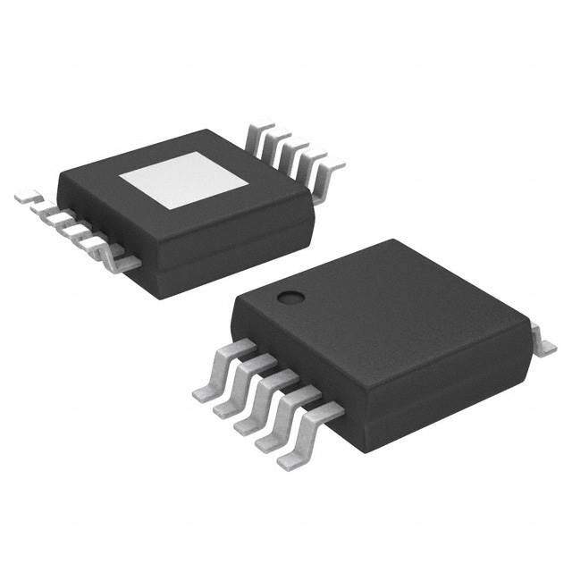
| 供应商器件封装 | 10-MSOP-PowerPad |
| 其它名称 | 296-36402-2 |
| 包装 | 带卷 (TR) |
| 同步整流器 | 无 |
| 商标 | Texas Instruments |
| 安装类型 | 表面贴装 |
| 安装风格 | SMD/SMT |
| 封装 | Reel |
| 封装/外壳 | 10-TFSOP,10-MSOP(0.118",3.00mm 宽)裸焊盘 |
| 封装/箱体 | HVSSOP-10 |
| 工作温度 | -40°C ~ 125°C |
| 工厂包装数量 | 250 |
| 开关频率 | 2.25 MHz |
| 拓扑结构 | Buck |
| 最大工作温度 | + 125 C |
| 最大输入电压 | 42 V |
| 最小工作温度 | - 40 C |
| 最小输入电压 | 6 V |
| 标准包装 | 250 |
| 电压-输入 | 6 V ~ 42 V |
| 电压-输出 | 2.51 V ~ 40 V |
| 电流-输出 | 2A |
| 类型 | Step-Down Regulators |
| 系列 | LM25011 |
| 输出数 | 1 |
| 输出电压 | 2.51 V to 40 V |
| 输出电流 | 2 A |
| 输出端数量 | 1 Output |
| 输出类型 | 可调式 |
| 频率-开关 | 最高 2MHz |


- 商务部:美国ITC正式对集成电路等产品启动337调查
- 曝三星4nm工艺存在良率问题 高通将骁龙8 Gen1或转产台积电
- 太阳诱电将投资9.5亿元在常州建新厂生产MLCC 预计2023年完工
- 英特尔发布欧洲新工厂建设计划 深化IDM 2.0 战略
- 台积电先进制程称霸业界 有大客户加持明年业绩稳了
- 达到5530亿美元!SIA预计今年全球半导体销售额将创下新高
- 英特尔拟将自动驾驶子公司Mobileye上市 估值或超500亿美元
- 三星加码芯片和SET,合并消费电子和移动部门,撤换高东真等 CEO
- 三星电子宣布重大人事变动 还合并消费电子和移动部门
- 海关总署:前11个月进口集成电路产品价值2.52万亿元 增长14.8%


PDF Datasheet 数据手册内容提取
Product Order Technical Tools & Support & Folder Now Documents Software Community LM25011,LM25011-Q1,LM25011A,LM25011A-Q1 SNVS617H–APRIL2009–REVISEDNOVEMBER2014 LM25011, LM25011-Q1, LM25011A, LM25011A-Q1 42-V 2-A Constant On-Time Switching Regulator With Adjustable Current Limit 1 Features 3 Description • LM25011-Q1isanAutomotiveGradeProductthat The LM25011 constant on-time step-down switching 1 regulator features all the functions needed to isAEC-Q100Grade1Qualified(–40°Cto+125°C implement a low-cost, efficient, buck bias regulator OperatingJunctionTemperature) capable of supplying up to 2 A of load current. This • LM25011AAllowsLow-DropoutOperationatHigh high-voltage regulator contains an N-Channel Buck SwitchingFrequency switch, a startup regulator, current limit detection, and • InputOperatingVoltageRange:6Vto42V internal ripple control. The constant on-time regulation principle requires no loop compensation, • AbsoluteMaximumInputRating:45V results in fast load transient response, and simplifies • Integrated2-AN-ChannelBuckSwitch circuit implementation. The operating frequency • AdjustableCurrentLimitAllowsforSmaller remains constant with line and load. The adjustable Inductor valley current limit detection results in a smooth transition from constant voltage to constant current • AdjustableOutputVoltagefrom2.51V mode when current limit is reached, without the use • MinimumRippleVoltageatV OUT of current limit foldback. The PGD output indicates • PowerGoodOutput the output voltage has increased to within 5% of the • SwitchingFrequencyAdjustableto2MHz expected regulation value. Additional features include: Low output ripple, VIN under-voltage lock- • COTTopologyFeatures: out, adjustable soft-start timing, thermal shutdown, – SwitchingFrequencyRemainsNearly gate drive pre-charge, gate drive under-voltage lock- ConstantwithLoadCurrentandInputVoltage out,andmaximumdutycyclelimit. Variations The LM25011A has a shorter minimum off-time than – Ultra-FastTransientResponse the LM25011, which allows for higher frequency – NoLoopCompensationRequired operationatlowinputvoltages. – StableOperationwithCeramicOutput DeviceInformation(1) Capacitors PARTNUMBER PACKAGE BODYSIZE(NOM) – AllowsforSmallerOutputCapacitorand LM25011/-Q1 CurrentSenseResistor HVSSOP(10) 3.00mm×3.00mm LM25011A/-Q1 • AdjustableSoft-StartTiming (1) For all available packages, see the orderable addendum at • ThermalShutdown theendofthedatasheet. • Precision2%FeedbackReference • Package:10-Pin,HVSSOP TypicalApplication • CreateaCustomDesignUsingtheLM25011 6V to 42V Input FamilywiththeWEBENCHPowerDesigner VIN BST LM25011 CBST L1 2 Applications CIN RT SW D1 • AutomotiveSafety RT • Infotainment RPGD CS VOUT VPGD • Telecommunication Power PGD RS COUT Good CSG RFB2 • FrontCamera SS CSS SGND FB RFB1 1 An IMPORTANT NOTICE at the end of this data sheet addresses availability, warranty, changes, use in safety-critical applications, intellectualpropertymattersandotherimportantdisclaimers.PRODUCTIONDATA.
LM25011,LM25011-Q1,LM25011A,LM25011A-Q1 SNVS617H–APRIL2009–REVISEDNOVEMBER2014 www.ti.com Table of Contents 1 Features.................................................................. 1 7.4 DeviceFunctionalModes........................................15 2 Applications........................................................... 1 8 ApplicationandImplementation........................ 16 3 Description............................................................. 1 8.1 ApplicationInformation............................................16 4 RevisionHistory..................................................... 2 8.2 TypicalApplication..................................................16 5 PinConfigurationandFunctions......................... 3 9 PowerSupplyRecommendations...................... 23 6 Specifications......................................................... 4 10 Layout................................................................... 23 6.1 AbsoluteMaximumRatings .....................................4 10.1 LayoutGuidelines.................................................23 6.2 HandlingRatings:LM25011......................................4 10.2 LayoutExample....................................................23 6.3 HandlingRatings:LM25011-Q1................................4 10.3 PowerDissipation.................................................23 6.4 RecommendedOperatingConditions.......................4 11 DeviceandDocumentationSupport................. 24 6.5 ThermalInformation..................................................5 11.1 CustomDesignwithWEBENCHTools.................24 6.6 ElectricalCharacteristics...........................................6 11.2 ReceivingNotificationofDocumentationUpdates24 6.7 TypicalCharacteristics..............................................7 11.3 RelatedLinks........................................................24 7 DetailedDescription............................................ 10 11.4 Trademarks...........................................................24 7.1 Overview.................................................................10 11.5 ElectrostaticDischargeCaution............................24 7.2 FunctionalBlockDiagram.......................................10 11.6 Glossary................................................................24 7.3 FeatureDescription.................................................10 12 Mechanical,Packaging,andOrderable Information........................................................... 24 4 Revision History NOTE:Pagenumbersforpreviousrevisionsmaydifferfrompagenumbersinthecurrentversion. ChangesfromRevisionG(February2013)toRevisionH Page • AddedPinConfigurationandFunctionssection,HandlingRatingtable,FeatureDescriptionsection,Device FunctionalModes,ApplicationandImplementationsection,PowerSupplyRecommendationssection,Layout section,DeviceandDocumentationSupportsection,andMechanical,Packaging,andOrderableInformation section ................................................................................................................................................................................... 1 ChangesfromRevisionF(February2013)toRevisionG Page • ChangedlayoutofNationalSemiconductorDataSheettoTIformat.................................................................................. 23 2 SubmitDocumentationFeedback Copyright©2009–2014,TexasInstrumentsIncorporated ProductFolderLinks:LM25011 LM25011-Q1 LM25011A LM25011A-Q1
LM25011,LM25011-Q1,LM25011A,LM25011A-Q1 www.ti.com SNVS617H–APRIL2009–REVISEDNOVEMBER2014 5 Pin Configuration and Functions 10-Pin HVSSOPPackage TopView Exposed Pad on Bottom Connect to Ground VIN 1 10 BST RT 2 9 SW PGD 3 8 CS SS 4 7 CSG SGND 5 6 FB PinFunctions PIN I/O DESCRIPTION APPLICATIONINFORMATION NUMBER NAME 1 VIN I Inputsupplyvoltage Operatinginputrangeis6Vto42V.Transientcapabilityis45V. AlowESRcapacitormustbeplacedascloseaspossibletothe VINandSGNDpins. 2 RT I On-timeControl AnexternalresistorfromVINtothispinsetsthebuckswitchon- timeandtheswitchingfrequency. 3 PGD – PowerGood LogicoutputindicateswhenthevoltageattheFBpinhas increasedtoabove95%oftheinternalreferencevoltage. Hysteresisisprovided.Anexternalpull-upresistortoavoltage lessthan7Visrequired. 4 SS I Soft-Start Aninternalcurrentsourcechargesanexternalcapacitorto providethesoft-startfunction. 5 SGND SignalGround Groundforallinternalcircuitryotherthanthecurrentlimitsense circuit. 6 FB I Feedback Internallyconnectedtotheregulationcomparator.Theregulation levelis2.51V. 7 CSG – CurrentSenseGround Groundconnectionforthecurrentlimitsensingcircuit.Connectto groundandtothecurrentsenseresistor. 8 CS I Currentsense Connecttothecurrentsenseresistorandtheanodeofthefree- wheelingdiode. 9 SW O SwitchingNode Internallyconnectedtothebuckswitchsource.Connecttothe externalinductor,cathodeofthefree-wheelingdiode,and bootstrapcapacitor. 10 BST I Bootstrapcapacitorconnectionof Connecta0.1-µFcapacitorfromSWtothispin.Thecapacitoris thebuckswitchgatedriver. chargedduringthebuckswitchoff-timeviaaninternaldiode. - EP – ExposedPad Exposedpadontheundersideofthepackage.Thispadshould besolderedtothePCboardgroundplanetoaidinheat dissipation. Copyright©2009–2014,TexasInstrumentsIncorporated SubmitDocumentationFeedback 3 ProductFolderLinks:LM25011 LM25011-Q1 LM25011A LM25011A-Q1
LM25011,LM25011-Q1,LM25011A,LM25011A-Q1 SNVS617H–APRIL2009–REVISEDNOVEMBER2014 www.ti.com 6 Specifications 6.1 Absolute Maximum Ratings(1) MIN MAX UNIT VINtoSGND(T =25°C) 45 V J BSTtoSGND 52 V SWtoSGND(SteadyState) –1.5 45 V BSTtoSW –0.3 7 V CStoCSG –0.3 0.3 V CSGtoSGND –0.3 0.3 V PGDtoSGND –0.3 7 V SStoSGND –0.3 3 V RTtoSGND –0.3 1 V FBtoSGND –0.3 7 V Forsolderingspecs,seewww.ti.com/packaging. JunctionTemperature 150 °C (1) AbsoluteMaximumRatings(1)arelimitsbeyondwhichdamagetothedevicemayoccur.RecommendedOperatingConditionsare conditionsunderwhichoperationofthedeviceisintendedtobefunctional.Forspecificationsandtestconditions,seetheElectrical Characteristics. 6.2 Handling Ratings: LM25011 MIN MAX UNIT T Storagetemperaturerange –65 150 °C stg Humanbodymodel(HBM),perANSI/ESDA/JEDECJS-001, 2000 allpins(1) V Electrostaticdischarge V (ESD) Chargeddevicemodel(CDM),perJEDECspecification 750 JESD22-C101,allpins(2) (1) JEDECdocumentJEP155statesthat500-VHBMallowssafemanufacturingwithastandardESDcontrolprocess. (2) JEDECdocumentJEP157statesthat250-VCDMallowssafemanufacturingwithastandardESDcontrolprocess. 6.3 Handling Ratings: LM25011-Q1 MIN MAX UNIT T Storagetemperaturerange –65 150 °C stg Humanbodymodel(HBM),perAECQ100-002(1) 2000 Cornerpins(1,5,6, 750 V(ESD) Electrostaticdischarge Chargeddevicemodel(CDM),per and10) V AECQ100-011 Otherpins 750 (1) AECQ100-002indicatesHBMstressingisdoneinaccordancewiththeANSI/ESDA/JEDECJS-001specification. 6.4 Recommended Operating Conditions overoperatingfree-airtemperaturerange(unlessotherwisenoted)(1) MIN MAX UNIT VINVoltage 6.0 42 V JunctionTemperature –40 125 °C (1) AbsoluteMaximumRatings(1)arelimitsbeyondwhichdamagetothedevicemayoccur.RecommendedOperatingConditionsare conditionsunderwhichoperationofthedeviceisintendedtobefunctional.Forspecificationsandtestconditions,seetheElectrical Characteristics. 4 SubmitDocumentationFeedback Copyright©2009–2014,TexasInstrumentsIncorporated ProductFolderLinks:LM25011 LM25011-Q1 LM25011A LM25011A-Q1
LM25011,LM25011-Q1,LM25011A,LM25011A-Q1 www.ti.com SNVS617H–APRIL2009–REVISEDNOVEMBER2014 6.5 Thermal Information HVSSOP(DGQ) THERMALMETRIC(1) UNIT 10PINS R Junction-to-ambientthermalresistance 48 θJA R Junction-to-case(top)thermalresistance 54.3 θJC(top) R Junction-to-boardthermalresistance 34.2 θJB °C/W ψ Junction-to-topcharacterizationparameter 4.0 JT ψ Junction-to-boardcharacterizationparameter 33.9 JB R Junction-to-case(bottom)thermalresistance 10 θJC(bot) (1) Formoreinformationabouttraditionalandnewthermalmetrics,seetheICPackageThermalMetricsapplicationreport,SPRA953. Copyright©2009–2014,TexasInstrumentsIncorporated SubmitDocumentationFeedback 5 ProductFolderLinks:LM25011 LM25011-Q1 LM25011A LM25011A-Q1
LM25011,LM25011-Q1,LM25011A,LM25011A-Q1 SNVS617H–APRIL2009–REVISEDNOVEMBER2014 www.ti.com 6.6 Electrical Characteristics TypicalvaluescorrespondtoT =25°C.Minimumandmaximumlimitsapplyover–40°Cto125°Cjunctiontemperaturerange J unlessotherwisestated.Unlessotherwisestated,thefollowingconditionsapply:V =12V,R =50kΩ.(1) (2) (3) IN T PARAMETER TESTCONDITIONS MIN TYP MAX UNIT INPUT(VINPIN) I Inputoperatingcurrent Non-switching,FB=3V 1200 1600 µA IN UVLO V undervoltagelock-outthreshold V increasing 4.6 5.3 5.9 V VIN IN IN V undervoltagelock-outthresholdhysteresis 200 mV IN SWITCHCHARACTERISTICS R BuckSwitchR I =200mA 0.3 0.6 Ω DS(ON) DS(ON) TEST UVLO GateDriveUVLO BST-SW 2.4 3.4 4.4 V GD UVLO Hysteresis 350 mV GD Pre-chargeswitchvoltage I =10mAintoSWpin 1.4 V TEST Pre-chargeswitchon-time 120 ns SOFT-STARTPIN V Pullupvoltage 2.51 V SS I Internalcurrentsource 10 µA SS V Shutdownthreshold 70 140 mV SS-SH CURRENTLIMIT V ThresholdvoltageatCS –146 –130 –115 mV ILIM CSbiascurrent FB=3V –120 µA CSGbiascurrent FB=3V –35 µA ONTIMER,RTPIN t -1 On-time V =12V,R =50kΩ 150 200 250 ns ON IN T t -2 On-time V =32V,R =50kΩ 75 ns ON IN T t -3 On-time(currentlimit)LM25011 V =12V,R =50kΩ 100 ns ON IN T t -3 On-time(currentlimit)LM25011A V =12V,R =50kΩ 200 ns ON IN T t -4 On-time V =12V,R =301kΩ 1020 ns ON IN T t -5 On-time V =9V,R =30.9kΩ 130 171 215 ns ON IN T t -6 On-time V =12V,R =30.9kΩ 105 137 170 ns ON IN T t -7 On-time V =16V,R =30.9kΩ 79 109 142 ns ON IN T OFFTIMER t Minimumoff-time(LM25011) 90 150 208 ns OFF Minimumoff-time(LM25011A) 52 75 93 REGULATIONCOMPARATOR(FBPIN) V FBregulationthreshold SSpin=steadystate 2.46 2.51 2.56 V REF FBbiascurrent FB=3V 100 nA POWERGOOD(PGDPIN) ThresholdatFB,withrespecttoV FBincreasing 91% 95% REF Thresholdhysteresis 3.3% PGD Lowstatevoltage I =1mA,FB=0V 125 180 mV VOL PGD PGD Offstateleakage V =7V,FB=3V 0.1 µA LKG PGD THERMALSHUTDOWN T Thermalshutdown Junctiontemperatureincreasing 155 °C SD Thermalshutdownhysteresis 20 °C (1) Currentflowoutofapinisindicatedasanegativenumber. (2) Allhotandcoldlimitsarespecifiedbycorrelatingtheelectricalcharacteristicstoprocessandtemperaturevariationsandapplying statisticalprocesscontrol. (3) Thejunctiontemperature(T in°C)iscalculatedfromtheambienttemperature(T in°C)andpowerdissipation(P inwatts)asfollows: J A D T =T +(P ×R )whereR (in°C/W)isthepackagethermalimpedanceprovidedintheThermalInformationsection. J A D θJA θJA 6 SubmitDocumentationFeedback Copyright©2009–2014,TexasInstrumentsIncorporated ProductFolderLinks:LM25011 LM25011-Q1 LM25011A LM25011A-Q1
LM25011,LM25011-Q1,LM25011A,LM25011A-Q1 www.ti.com SNVS617H–APRIL2009–REVISEDNOVEMBER2014 6.7 Typical Characteristics Figure1.Efficiency(CircuitofFigure19) Figure2.Efficiencyat2MHz Figure3.On-TimevsV andR Figure4.VoltageattheRTPin IN T Figure5.ShutdownCurrentintoVIN Figure6.OperatingCurrentintoVIN Copyright©2009–2014,TexasInstrumentsIncorporated SubmitDocumentationFeedback 7 ProductFolderLinks:LM25011 LM25011-Q1 LM25011A LM25011A-Q1
LM25011,LM25011-Q1,LM25011A,LM25011A-Q1 SNVS617H–APRIL2009–REVISEDNOVEMBER2014 www.ti.com Typical Characteristics (continued) Figure7.PGDLowVoltagevsSinkCurrent Figure8.ReferenceVoltagevsTemperature Figure9.CurrentLimitThresholdvsTemperature Figure10.OperatingCurrentvsTemperature Figure11.VINUVLOvsTemperature Figure12.SSPinShutdownThresholdvsTemperature 8 SubmitDocumentationFeedback Copyright©2009–2014,TexasInstrumentsIncorporated ProductFolderLinks:LM25011 LM25011-Q1 LM25011A LM25011A-Q1
LM25011,LM25011-Q1,LM25011A,LM25011A-Q1 www.ti.com SNVS617H–APRIL2009–REVISEDNOVEMBER2014 Typical Characteristics (continued) 190 170 s) E (n 150 LM25011 M TI 130 F- F O M 110 U M NI 90 LM25011A MI 70 50 -40 -20 0 20 40 60 80 100 120 JUNCTION TEMPERATURE (°C) Figure13.On-TimevsTemperature Figure14.MinimumOff-TimevsTemperature Copyright©2009–2014,TexasInstrumentsIncorporated SubmitDocumentationFeedback 9 ProductFolderLinks:LM25011 LM25011-Q1 LM25011A LM25011A-Q1
LM25011,LM25011-Q1,LM25011A,LM25011A-Q1 SNVS617H–APRIL2009–REVISEDNOVEMBER2014 www.ti.com 7 Detailed Description 7.1 Overview The LM25011 constant on-time step-down switching regulator features all the functions needed to implement a low-cost, efficient buck bias power converter capable of supplying up to 2.0 A to the load. This high-voltage regulator contains an N-Channel buck switch, is easy to implement, and is available in a 10-pin VSSOP, PowerPAD power enhanced package. The operation of the regulator is based on a constant on-time control principle with the on-time inversely proportional to the input voltage. This feature results in the operating frequency remaining relatively constant with load and input voltage variations. The constant on-time feedback control principle requires no loop compensation resulting in very fast load transient response. The adjustable valley current limit detection results in a smooth transition from constant voltage to constant current when current limitisreached.Toaidincontrollingexcessiveswitchcurrentduetoapossiblesaturatinginductor,theon-timeis reduced by approximately 40% when the current limit is detected. The Power Good output (PGD pin) indicates whentheoutputvoltageiswithin5%oftheexpectedregulationvoltage. The LM25011 can be implemented to efficiently step-down higher voltages in non-isolated applications. Additional features include: low output ripple, VIN under-voltage lock-out, adjustable soft-start timing, thermal shutdown,gatedrivepre-charge,gatedriveunder-voltagelock-out,andmaximumduty-cyclelimit. 7.2 Functional Block Diagram 6V to 42V VIN LM25011(A) 5V REGULATOR Input CIN CBYP CL UVLO RT THERMAL ON TIMER OFF TIMER SHUTDOWN RT FINISH START START FINISH BST 2.5V Gate Drive SD 10 VIN PA UVLO CBST SS CSS LOGIC LEVEL SHIFT L1 VOUT FCIC SW CONTROL FB + CL + Pre-Chg D1 COUT - REGULATION CURRENT - RFB2 COMPARATOR LIMIT COMPARATOR CS RPGD PGoowoedr PGD - 0.8V CTUHRRREESNHTO LLIDMIT +- 125 mV RS CSG RFB2 + 2.375V SGND 7.3 Feature Description 7.3.1 ControlCircuitOverview The LM25011 buck regulator employs a control principle based on a comparator and a one-shot on-timer, with the output voltage feedback (FB) compared to an internal reference (2.51 V). If the FB voltage is below the reference, the internal buck switch is switched on for the one-shot timer period which is a function of the input voltage and the programming resistor (R ). Following the on-time, the switch remains off until the FB voltage falls T below the reference, but never less than the minimum off-time forced by the off-time one-shot timer. When the FB pin voltage falls below the reference and the off-time one-shot period expires, the buck switch is then turned onforanotheron-timeone-shotperiod. 10 SubmitDocumentationFeedback Copyright©2009–2014,TexasInstrumentsIncorporated ProductFolderLinks:LM25011 LM25011-Q1 LM25011A LM25011A-Q1
LM25011,LM25011-Q1,LM25011A,LM25011A-Q1 www.ti.com SNVS617H–APRIL2009–REVISEDNOVEMBER2014 Feature Description (continued) When in regulation, the LM25011 operates in continuous conduction mode at heavy load currents and discontinuous conduction mode at light load currents. In continuous conduction mode, the inductor current is always greater than zero and the operating frequency remains relatively constant with load and line variations. The minimum load current for continuous conduction mode is one-half of the ripple current amplitude of the inductor.Theapproximateoperatingfrequencyiscalculatedasfollows: V OUT F = S (4.1 x 10⁻¹¹ x (R + 0.5k)) + (V x 15 ns) T IN (1) Thebuckswitchdutycycleisapproximatelyequalto: tON VOUT DC = tON + tOFF = tON x FS = VIN (2) When the load current is less than one-half of the ripple current amplitude of the inductor, the circuit operates in discontinuous conduction mode. The off-time is longer than in continuous conduction mode while the inductor currentiszero,causingtheswitchingfrequencytoreduceastheloadcurrentisreduced.Conversionefficiencyis maintainedatlightloadsbecausetheswitchinglossesarereducedwiththereductioninloadandfrequency.The approximatediscontinuousoperatingfrequencycanbecalculatedasfollows: V 2 x L1 x 1.19 x 1021 OUT F = S 2 R x R L T (3) whereR =theloadresistance,andL1istheinductorinthecircuit. L The output voltage is set by the two feedback resistors (R , R in the Functional Block Diagram ). The FB1 FB2 regulatedoutputvoltageiscalculatedasfollows: V =2.51V×(R +R )/R (4) OUT FB1 FB2 FB1 Ripple voltage, which is required at the input of the regulation comparator for proper output regulation, is generated internally in the LM25011, and externally when the LM25011A is used. In the LM25011 the ERM (emulated ripple mode) control circuit generates the required internal ripple voltage from the ripple waveform at the CS pin. The LM25011A, which is designed for higher frequency operation, requires additional ripple voltage which must be generated externally and provided to the FB pin. This is described in the Application and Implementationsection. 7.3.2 On-TimeTimer The on-time for the LM25011/LM25011A is determined by the R resistor and the input voltage (V ), calculated T IN from: 4.1 x 10⁻¹¹ x (R + 500:) T t = + 15 ns ON (V ) IN (5) The inverse relationship with V results in a nearly constant frequency as V is varied. To set a specific IN IN continuousconductionmodeswitchingfrequency(F ),theR resistorisdeterminedfromthefollowing: S T V - (V x F x 15 ns) R = OUT IN S - 500: T -11 F x 4.1 x 10 S (6) Theon-timemustbechosengreaterthan90nsforproperoperation.Equation1,Equation5,andEquation6are valid only during normal operation; that is, the circuit is not in current limit. When the LM25011 operates in currentlimit,theon-timeisreducedbyapproximately40%(thisfeatureisnotpresentinLM25011A).Thisfeature reduces the peak inductor current which may be excessively high if the load current and the input voltage are simultaneously high. This feature operates on a cycle-by-cycle basis until the load current is reduced and the Copyright©2009–2014,TexasInstrumentsIncorporated SubmitDocumentationFeedback 11 ProductFolderLinks:LM25011 LM25011-Q1 LM25011A LM25011A-Q1
LM25011,LM25011-Q1,LM25011A,LM25011A-Q1 SNVS617H–APRIL2009–REVISEDNOVEMBER2014 www.ti.com Feature Description (continued) output voltage resumes its normal regulated value. The maximum continuous current into the RT pin must be less than 2 mA. For high-frequency applications, the maximum switching frequency is limited at the maximum input voltage by the minimum on-time one-shot period (90 ns). At minimum input voltage the maximum switching frequency is limited by the minimum off-time one-shot period which, if reached, prevents achievement of the properdutycycle. 7.3.3 CurrentLimit Current limit detection occurs during the off-time by monitoring the voltage across the external current sense resistor R . Referring to the Functional Block Diagram , during the off-time the recirculating current flows through S the inductor, through the load, through the sense resistor, and through D1 to the inductor. If the voltage across the sense resistor exceeds the threshold (V ), the current limit comparator output switches to delay the start of ILIM the next on-time period. The next on-time starts when the recirculating current decreases such that the voltage across R reduces to the threshold and the voltage at FB is below 2.51 V. The operating frequency is typically S lower due to longer-than-normal off-times. When current limit is detected, the on-time is reduced by approximately 40% (only in LM25011) if the voltage at the FB pin is below its threshold when the voltage across R reducestoitsthreshold(V islowduetocurrentlimiting). S OUT Figure 15 illustrates the inductor current waveform during normal operation and in current limit. During the first normal operation, the load current is I , the average of the inductor current waveform. As the load resistance is 01 reduced, the inductor current increases until the lower peak of the inductor ripple current exceeds the threshold. During the current limited portion of Figure 15, each on-time is reduced by approximately 40%, resulting in lower ripple amplitude for the inductor current. During this time the LM25011 is in a constant-current mode with an average load current equal to the current limit threshold plus half the ripple amplitude (I ), and the output OCL voltageisbelowthenormalregulatedvalue.Normaloperationresumeswhentheloadcurrentisreduced(toI ), O2 allowing V and the on-time to return to their normal values. Note that in the second period of normal OUT operation, even though the peak current of the inductor exceeds the current limit threshold during part of each cycle, the circuit is not in current limit because the inductor current falls below the current limit threshold during each off-time. The peak current allowed through the buck switch is 3.5 A and the maximum allowed average currentis2.0A. IPK IOCL Current ’I IO2 LimitThreshold Inductor Current IO1 0V Voltage at the CS Pin Voltage at the FB Pin 2.51V Load Normal Current Current Normal Operation Increases Limited Load Current Operation Decreases Figure15. NormalandCurrentLimitOperation 12 SubmitDocumentationFeedback Copyright©2009–2014,TexasInstrumentsIncorporated ProductFolderLinks:LM25011 LM25011-Q1 LM25011A LM25011A-Q1
LM25011,LM25011-Q1,LM25011A,LM25011A-Q1 www.ti.com SNVS617H–APRIL2009–REVISEDNOVEMBER2014 Feature Description (continued) 7.3.4 RippleRequirements The LM25011 requires about 25 mV of ripple voltage at the CS pin. Higher switching frequencies may require P-P more ripple. That ripple voltage is generated by the decreasing recirculating current (the inductor ripple current) throughR duringtheoff-time.SeeFigure16. S Inductor Current ’I 0V Voltage at CS V RIPPLE tOFF tON Figure16. CSPinWaveform Theripplevoltageisequalto: V =ΔI×R (7) RIPPLE S whereΔIistheinductorcurrentrippleamplitude,andR isthecurrent-senseresistorattheCSpin. S Moreripplecanbeachievedbydecreasingtheinductorvalue. The LM25011A, with its shorter minimum off-time, typically will require more ripple than the LM25011. An external circuit to increase the effective ripple voltage may be needed. Different methods of generating this ripple areexplainedintheExternalComponentssection. 7.3.5 N-ChannelBuckSwitchandDriver The LM25011 integrates an N-Channel buck switch and associated floating high-voltage gate driver. The gate driver circuit works in conjunction with an external bootstrap capacitor (C ) and an internal high-voltage diode. BST A 0.1-µF capacitor connected between BST and SW provides the supply voltage for the driver during the on- time. During each off-time, the SW pin is at approximately –1 V, and C is recharged from the internal 5-V BST regulator for the next on-time. The minimum off-time ensures a sufficient time each cycle to recharge the bootstrapcapacitor. Inapplicationswithrelativelyhighoutputvoltageandlowminimumloadcurrent,theinternalpre-chargedeviceof the LM25011 may not pull the SW pin sufficiently low during the off-time to maintain the voltage on the bootstrap capacitor. If the bootstrap capacitor (C ) discharges during the long off-times, and the regulator will cycle on BST and off at a low frequency. Decreasing the values of the feedback resistors R and R to provide a minimum FB1 FB2 load of typically 1mA at nominal V will increase the minimum switching frequency and maintain sufficient OUT bootstrapcapacitorvoltage. 7.3.6 Soft-Start The soft-start feature allows the converter to gradually reach a steady-state operating point, thereby reducing startup stresses and current surges. Upon turn-on, when V reaches its undervoltage lock-out threshold an IN internal 10-µA current source charges the external capacitor at the SS pin to 2.51 V (t1 in Figure 17). The ramping voltage at SS ramps the non-inverting input of the regulation comparator and the output voltage, in a controlledmanner.Forproperoperation,thesoft-startcapacitorshouldbenosmallerthan1000pF. Copyright©2009–2014,TexasInstrumentsIncorporated SubmitDocumentationFeedback 13 ProductFolderLinks:LM25011 LM25011-Q1 LM25011A LM25011A-Q1
LM25011,LM25011-Q1,LM25011A,LM25011A-Q1 SNVS617H–APRIL2009–REVISEDNOVEMBER2014 www.ti.com Feature Description (continued) The LM25011 can be employed as a tracking regulator by applying the controlling voltage to the SS pin. The output voltage of the regulator tracks the applied voltage, gained up by the ratio of the feedback resistors. The appliedvoltageattheSSpinmustbewithintherangeof0.5Vto2.6V.TheabsolutemaximumratingfortheSS pin is 3.0 V. If the tracking function causes the voltage at the FB pin to go below the thresholds for the PGD pin, thePGDpinwillswitchlow(seethePowerGoodOutput(PGD) section).AninternalswitchgroundstheSSpinif the input voltage at VIN is below its undervoltage lock-out threshold or if the thermal shutdown activates. If the tracking function (described above) is used, the tracking voltage applied to the SS pin must be current limited to amaximumof1mA. UVLO VIN SW Pin Inductor Current SS Pin VOUT PGD t1 Figure17. StartupSequence 7.3.7 PowerGoodOutput(PGD) The Power Good output (PGD) indicates when the voltage at the FB pin is close to the internal 2.51-V reference voltage.TherisingthresholdattheFBpinforthePGDoutputtoswitchhighis95%oftheinternalreference.The fallingthresholdforthePGDoutputtoswitchlowisapproximately3.3%belowtherisingthreshold. The PGD pin is internally connected to the drain of an N-channel MOSFET switch. An external pull-up resistor (R ), connected to an appropriate voltage not exceeding 7 V, is required at PGD to indicate the LM25011 PGD statustoothercircuitry.WhenPGDislow,thepinvoltageisdeterminedbythecurrentintothepin.SeeFigure7, PGDLowVoltagevsSinkCurrent. 14 SubmitDocumentationFeedback Copyright©2009–2014,TexasInstrumentsIncorporated ProductFolderLinks:LM25011 LM25011-Q1 LM25011A LM25011A-Q1
LM25011,LM25011-Q1,LM25011A,LM25011A-Q1 www.ti.com SNVS617H–APRIL2009–REVISEDNOVEMBER2014 Feature Description (continued) Upon powering up the LM25011, the PGD pin is high until the voltage at V reaches 2 V, at which time PGD IN switches low. As V is increased, PGD stays low until the output voltage takes the voltage at the FB pin above IN 95% of the internal reference voltage, at which time PGD switches high. As V is decreased (during shutdown), IN PGDremainshighuntileitherthevoltageattheFBpinfallsbelowapproximately92%oftheinternalreferenceor when V falls below its lower UVLO threshold, whichever occurs first. PGD then switches low, and remains low IN until V falls below 2 V, at which time PGD switches high. If the LM25011 is used as a tracking regulator (see IN the Soft-Start section), the PGD output is high as long as the voltage at the FB pin is above the thresholds mentionedabove. 7.3.8 ThermalShutdown The LM25011 should be operated so the junction temperature does not exceed 125°C. If the junction temperature increases above that, an internal thermal shutdown circuit activates (typically) at 155°C, taking the controller to a low-power reset state by disabling the buck switch and taking the SS pin to ground. This feature helpspreventcatastrophicfailuresfromaccidentaldeviceoverheating.Whenthejunctiontemperaturedecreases below135°C(typicalhysteresis=20°C),normaloperationresumes. 7.4 Device Functional Modes 7.4.1 ShutdownFunction The SS pin can be used to shutdown the LM25011 by grounding the SS pin as shown in Figure 18. Releasing thepinallowsnormaloperationtoresume. SS LM25011 STOP C SS RUN Figure18. ShutdownImplementation Copyright©2009–2014,TexasInstrumentsIncorporated SubmitDocumentationFeedback 15 ProductFolderLinks:LM25011 LM25011-Q1 LM25011A LM25011A-Q1
LM25011,LM25011-Q1,LM25011A,LM25011A-Q1 SNVS617H–APRIL2009–REVISEDNOVEMBER2014 www.ti.com 8 Application and Implementation NOTE Information in the following applications sections is not part of the TI component specification, and TI does not warrant its accuracy or completeness. TI’s customers are responsible for determining suitability of components for their purposes. Customers should validateandtesttheirdesignimplementationtoconfirmsystemfunctionality. 8.1 Application Information The LM25011/LM25011-Q1 is a non-synchronous buck regulator designed to operate over a wide input voltage range and output current. Spreadsheet-based quick-start calculation tools and the on-line WEBENCH® software can be used to create a buck design with the bill of materials, estimated efficiency, and the complete solution cost. 8.2 Typical Application 8.2.1 LM25011ExampleCircuit ThefinalcircuitisshowninFigure19,anditsperformanceisshowninFigure20andFigure21.Thecurrentlimit measuresapproximately1.62AatV =8V,and1.69AatV =36V. IN IN 8V to 36V Input BST CBYP VIN CBST 0.1 PF CIN RT 0.1 PF LM25011 L1 10 PH 4.7 PF 118 k: SW RT D1 VOUT 5V VPGD CS 1R0P kG:D RS C10O UPTF 80 m: Power PGD Good RFB2 CSG 4.99 k: SS CSS SGND FB 0.022 PF RFB1 4.99 k: Figure19. ExampleCircuit 8.2.1.1 DesignRequirements Table1showsthedesignparameters. Table1.DesignParameters DESIGNPARAMETER VALUE Inputvoltagerange 8Vto36V Outputvoltage 5V Maximumloadcurrent(I ) 1.5A OUT(max) Minimumloadcurrent(I ) 300mA OUT(min) Switchingfrequency(F ) 1MHz SW Soft-starttime 5ms 16 SubmitDocumentationFeedback Copyright©2009–2014,TexasInstrumentsIncorporated ProductFolderLinks:LM25011 LM25011-Q1 LM25011A LM25011A-Q1
LM25011,LM25011-Q1,LM25011A,LM25011A-Q1 www.ti.com SNVS617H–APRIL2009–REVISEDNOVEMBER2014 8.2.1.2 DetailedDesignProcedure 8.2.1.2.1 CustomDesignwithWEBENCHTools ClickheretocreateacustomdesignusingtheLM25011devicewiththe WEBENCH® PowerDesigner. 1. StartbyenteringyourV ,V andI requirements. IN OUT OUT 2. Optimize your design for key parameters like efficiency, footprint and cost using the optimizer dial and comparethisdesignwithotherpossiblesolutionsfromTexasInstruments. 3. WEBENCH Power Designer provides you with a customized schematic along with a list of materials with real timepricingandcomponentavailability. 4. Inmostcases,youwillalsobeableto: – Runelectricalsimulationstoseeimportantwaveformsandcircuitperformance, – Runthermalsimulationstounderstandthethermalperformanceofyourboard, – ExportyourcustomizedschematicandlayoutintopopularCADformats, – PrintPDFreportsforthedesign,andshareyourdesignwithcolleagues. 5. GetmoreinformationaboutWEBENCHtoolsatwww.ti.com/webench. 8.2.1.2.2 ExternalComponents The procedure for calculating the external components is illustrated with a design example using the LM25011. ReferringtotheFunctionalBlockDiagram,thecircuitistobeconfiguredforthefollowingspecifications: • V =5V OUT • V =8Vto36V IN • MinimumloadcurrentforcontinuousconductionmodeI =300mA OUT(min) • MaximumloadcurrentI =1.5A OUT(max) • Switchingfrequency(F )=1.0MHz SW • Soft-starttime=5ms R andR :Theseresistorssettheoutputvoltage,andtheirratioiscalculatedfrom: FB2 FB1 R /R =(V /2.51V)–1 (8) FB2 FB1 OUT For this example, R /R = 0.992. R and R should be chosen from standard value resistors in the range FB2 FB1 FB1 FB2 of1.0kΩ to10kΩ whichsatisfytheaboveratio.Forthisexample,4.99kΩ ischosenforbothresistors,providing a5.02-Voutput. R :This resistor sets the on-time and (by default) the switching frequency. First check that the desired frequency T does not require an on-time or off-time shorter than the minimum allowed values (90 ns and 150, respectively). Theminimumon-timeoccursatthemaximuminputvoltage.Forthisexample: V OUT 5V t = = = 139 ns ON(min) V x F 36V x 1 MHz IN(max) S (9) Theminimumoff-timeoccursattheminimuminputvoltage.Forthisexample: VIN(min) - VOUT 8V - 5V t = = = 375 ns OFF(min) V x F 8V x 1 MHz IN(min) S (10) Both the on-time and off-time are acceptable because they are significantly greater than the minimum value for each.TheR resistoriscalculatedfromEquation6usingtheminimuminputvoltage: T 5 - (8V x 1MHz x 15 ns) R = - 500:(cid:3)= 118.5 k: T -11 1MHz x 4.1 x 10 (11) A standard value 118-kΩ resistor is selected. The minimum on-time calculates to 152 ns at V = 36 V, and the IN maximumon-timecalculatesto672nsatV =8V. IN Copyright©2009–2014,TexasInstrumentsIncorporated SubmitDocumentationFeedback 17 ProductFolderLinks:LM25011 LM25011-Q1 LM25011A LM25011A-Q1
LM25011,LM25011-Q1,LM25011A,LM25011A-Q1 SNVS617H–APRIL2009–REVISEDNOVEMBER2014 www.ti.com L1: The parameters controlled by the inductor are the inductor current ripple amplitude (I ), and the ripple OR voltage amplitude across the current sense resistor R . The minimum load current is used to determine the S maximum allowable ripple to maintain continuous conduction mode (the lower peak does not reach 0 mA). This is not a requirement of the LM25011, but serves as a guideline for selecting L1. For this example, the maximum ripplecurrentshouldbelessthan: I =2×I =600mA (12) OR(max) OUT(min) P-P For applications where the minimum load current is zero, a good starting point for allowable ripple is 20% of the maximum load current. In this case substitute 20% of I for I in Equation 12. The ripple amplitude OUT(max) OUT(min) calculatedinEquation12isthenusedinEquation13: t x (V -V ) ON(min) IN(max) OUT L1 = = 7.85 PH (min) I OR(max) (13) A standard value 10-µH inductor is chosen. Using this inductor value, the maximum ripple current amplitude, which occurs at maximum V , calculates to 472 mA , and the peak current is 1736 mA at maximum load IN P-P current. Ensure the selected inductor is rated for this peak current. The minimum ripple current, which occurs at minimumV ,calculatesto200mA . IN P-P R : The minimum current limit threshold is calculated at maximum load current using the minimum ripple current S calculated above. The current limit threshold is the lower peak of the inductor current waveform when in current limit(seeFigure15). I =1.5A–(0.2A/2)=1.4A (14) LIM Currentlimitdetectionoccurswhenthevoltageacrossthesenseresistor(R )reachesthecurrentlimitthreshold. S Toallowfortolerances,thesenseresistorvalueiscalculatedusingtheminimumthresholdspecification: R =115mV/1.4A=82mΩ (15) S The next smaller standard value, 80 mΩ, is selected. The next step is to ensure that sufficient ripple voltage occurs across R with this value sense resistor. As mentioned in the Ripple Requirements section, a minimum of S 15-mV voltage ripple is required across the R sense resistor during the off-time to ensure the regulation P-P S circuit operates properly. The ripple voltage is the product of the inductor ripple current amplitude and the sense resistorvalue.Inthiscase,theminimumripplevoltagecalculatesto: V =ΔI×R =200mA×0.080Ω=16mV (16) RIPPLE S If the ripple voltage had calculated to less than 15 mV , the inductor value would have to be reduced to P-P increase the ripple current amplitude. This would have required a recalculation of I and R in the above LIM S equations.Becausetheminimumrequirementissatisfiedinthiscase,nochangeisnecessary. Thenominalcurrentlimitthresholdcalculatesto1.63A.Theminimumandmaximumthresholdscalculateto1.44 A and 1.83 A, respectively, using the minimum and maximum limits for the current limit threshold specification. The load current is equal to the threshold current plus one-half of the ripple current. Under normal load conditions,themaximumpowerdissipationinR occursatmaximumloadcurrent,andatmaximuminputvoltage S wheretheon-timedutycycleisminimum.Inthisdesignexample,theminimumon-timedutycycleis: VOUT 5V Duty Cycle = D = = = 13.9% V 36V IN (17) Atmaximumloadcurrent,thepowerdissipationinR isequalto: S P =(1.5A)2×0.080Ω×(1–0.139)=155mW (18) (RS) WhenincurrentlimitthemaximumpowerdissipationinR calculatesto S P =(1.83A+0.472A/4)2×0.080Ω=304mW (19) (RS) Duty cycle is not included in this power calculation because the on-time duty cycle is typically <5% when in currentlimit. C : The output capacitor should typically be no smaller than 3.3 µF, although that is dependent on the OUT frequency and the desired output characteristics. C should be a low ESR good-quality ceramic capacitor. OUT Experimentation is usually necessary to determine the minimum value for C , as the nature of the load may OUT require a larger value. A load which creates significant transients requires a larger value for C than a non- OUT varyingload. 18 SubmitDocumentationFeedback Copyright©2009–2014,TexasInstrumentsIncorporated ProductFolderLinks:LM25011 LM25011-Q1 LM25011A LM25011A-Q1
LM25011,LM25011-Q1,LM25011A,LM25011A-Q1 www.ti.com SNVS617H–APRIL2009–REVISEDNOVEMBER2014 C and C :The purpose of C is to supply most of the switch current during the on-time, and limit the voltage IN BYP IN ripple at V , because it is assumed the voltage source feeding V has some amount of source impedance. IN IN When the buck switch turns on, the current into V suddenly increases to the lower peak of the inductor ripple IN current,thenrampsuptotheupperpeak,andfinallydropstozeroatturn-off.Theaveragecurrentduringtheon- time is the average load current. For a worst case calculation, C must supply this average load current during IN the maximum on-time, without letting the voltage at the VIN pin drop below a minimum operating level of 5.5 V. For this exercise 0.5 V is chosen as the maximum allowed input ripple voltage. Using the maximum load current, theminimumvalueforC iscalculatedfrom: IN IOUT(max) x tON(max) 1.5A x 672 ns C = = = 2.02 PF IN ’V 0.5V (20) where t is the maximum on-time, and ΔV is the allowable ripple voltage at V . The purpose of C is to ON IN BYP minimize transients and ringing due to long lead inductance leading to the VIN pin. A low ESR 0.1-µF ceramic chipcapacitorisrecommended,andC mustbelocatedclosetotheVINandSGNDpins. BYP C : The recommended value for C is 0.1 µF. A high-quality ceramic capacitor with low ESR is BST BST recommended as C supplies a surge current to charge the buck switch gate at each turn-on. A low ESR also BST helpsensureacompleterechargeduringeachoff-time. C :ThecapacitorattheSSpindeterminesthesoft-starttime,thatis,thetimefortheoutputvoltagetoreachits SS finalvalue(t1inFigure17).Forasoft-starttimeof5ms,thecapacitorvalueisdeterminedfromthefollowing: 5 ms x 10 PA C = = 0.02 PF SS 2.51V (21) D1: A Schottky diode is recommended. Ultra-fast recovery diodes are not recommended as the high-speed transitions at the SW pin may affect the regulator operation due to the reverse recovery transients of the diode. The diode must be rated for the maximum input voltage, the maximum load current, and the peak current which occurs when the current limit and maximum ripple current are reached simultaneously. The average power dissipationofthediodeiscalculatedfrom: P =V ×I ×(1–D) (22) D1 F OUT whereV istheforwardvoltagedropofthediode,andDistheon-timedutycycle. F 8.2.1.3 ApplicationCurves Figure20.Efficiency(CircuitofFigure19) Figure21.FrequencyvsV (CircuitofFigure19) IN Copyright©2009–2014,TexasInstrumentsIncorporated SubmitDocumentationFeedback 19 ProductFolderLinks:LM25011 LM25011-Q1 LM25011A LM25011A-Q1
LM25011,LM25011-Q1,LM25011A,LM25011A-Q1 SNVS617H–APRIL2009–REVISEDNOVEMBER2014 www.ti.com 8.2.2 OutputRippleControl High frequency applications of the LM25011 or LM25011A are likely to require more ripple voltage than is internally generated across the R resistor. Additional ripple can be supplied to the FB pin, in phase with the S switching waveform at the SW pin, for proper operation. The required ripple can be supplied from ripple generated at V , through the feedback resistors, as described in Option A: Lowest Cost Configuration . Option OUT B: Intermediate V Ripple Configuration and Option C: Minimum V Ripple Configuration use one or two OUT OUT additionalcomponentstoproviderippleattheFBpinwithloweroutputrippleatV . OUT TheamountofadditionalripplevoltageneededattheFBpinistypicallyintherangeof30mVto150mV.Higher switching frequencies or higher inductor values (less ripple current) require more external ripple voltage injected at the FB pin. Insufficient ripple voltage will result in frequency jitter. For a particular application, add only as muchrippleasneededtostabilizetheswitchingfrequencyovertherequiredinputvoltage. 8.2.2.1 OptionA:LowestCostConfiguration In this configuration R1 is installed in series with the output capacitor (C ) as shown in Figure 22. The ripple OUT currentoftheinductorpassesthroughR1,generatingaripplevoltageatV .TheminimumvalueforR1is: OUT V x (R + R ) RIPPLE FB2 FB1 R1 = ’I x R FB1 (23) where ΔI is the minimum ripple current amplitude, which occurs at minimum V , and V is the peak to peak IN RIPPLE ripplevoltageinjectedattheFBpin. BST C LM25011A BST L1 SW V OUT D1 CS RFB2 R1 RS C OUT CSG R FB FB1 SGND Figure22. OptionA – LowestCostRippleConfiguration 8.2.2.2 OptionB:IntermediateV RippleConfiguration OUT This configuration generates less ripple at V than Option A by the addition of capacitor (Cff) as shown in OUT Figure23. BecausetheoutputrippleispassedbyCfftotheFBpinwithlittleornoattenuation,theR1valueandV ripple OUT canbesmallerthaninOptionA.TheminimumvalueforR1iscalculatedfrom: V R1 = RIPPLE ’I (24) where ΔI is the minimum ripple current amplitude, which occurs at minimum V , and V is the peak-to-peak IN RIPPLE ripplevoltageinjectedattheFBpin.TheminimumvalueforCffiscalculatedfrom: 3 x t ON(max) Cff > R //R FB1 FB2 (25) wheret isthemaximumon-time(atminimumV ),andR //R istheparallelequivalentofthefeedback ON(max) IN FB1 FB2 resistors. 20 SubmitDocumentationFeedback Copyright©2009–2014,TexasInstrumentsIncorporated ProductFolderLinks:LM25011 LM25011-Q1 LM25011A LM25011A-Q1
LM25011,LM25011-Q1,LM25011A,LM25011A-Q1 www.ti.com SNVS617H–APRIL2009–REVISEDNOVEMBER2014 BST CBST LM25011A L1 SW VOUT D1 CS R1 Cff RFB2 RS COUT CSG FB RFB1 SGND Figure23. OptionB – IntermediateRippleConfiguration Copyright©2009–2014,TexasInstrumentsIncorporated SubmitDocumentationFeedback 21 ProductFolderLinks:LM25011 LM25011-Q1 LM25011A LM25011A-Q1
LM25011,LM25011-Q1,LM25011A,LM25011A-Q1 SNVS617H–APRIL2009–REVISEDNOVEMBER2014 www.ti.com 8.2.2.3 OptionC:MinimumV RippleConfiguration OUT In some applications, the V ripple induced by series resistor R1 may not be acceptable. When low V ripple OUT OUT is required, an external ripple circuit, as shown in Figure 24, can be used to provide the required ripple at the FB pin. 1. The time constant Rr × Cr should be more than 8 to 10 times the switching period to generate a triangular waveformatthejunctionofRr,CrandCac. 2. TheminimumrippleatFB(atminimumV )isequalto:V =(V –V )×T /(RrxCr). IN RIPPLE IN(min) OUT ON(max) 3. The ripple capacitor Cr should much smaller than the ac coupling capacitor Cac. Typically Cac = 100 nF, Cr =1nF,andRrischosentosatisfyconditions1and2above. BST C LM25011A BST L1 SW VOUT D1 Rr Cr CS Cac COUT RS CSG FB RFB1 SGND Figure24. OptionC:MinimumOutputRippleConfiguration 22 SubmitDocumentationFeedback Copyright©2009–2014,TexasInstrumentsIncorporated ProductFolderLinks:LM25011 LM25011-Q1 LM25011A LM25011A-Q1
LM25011,LM25011-Q1,LM25011A,LM25011A-Q1 www.ti.com SNVS617H–APRIL2009–REVISEDNOVEMBER2014 9 Power Supply Recommendations The LM25011 is designed to operate with an input power supply capable of supplying a voltage range between 6 V and 42 V. The power supply should be well regulated and capable of supplying sufficient current to the regulator during peak load operation. Also, like in all applications, the power supply source impedance must be smallcomparedtothemoduleinputimpedancetomaintainthestabilityoftheconverter. 10 Layout 10.1 Layout Guidelines The LM25011 regulation and current limit comparators are very fast, and respond to short-duration noise pulses. Layout considerations are therefore critical for optimum performance. The layout must be as neat and compact as possible, and all of the components must be as close as possible to their associated pins. The two major current loops conduct currents which switch very fast, and therefore those loops must be as small as possible to minimize conducted and radiated EMI. The first loop is formed by C , through the VIN to SW pins, L , C , IN IND OUT and back to C . The second current loop is formed by R , D1, L , C , and back to R . The ground IN S IND OUT S connectionfromCSGtothegroundendofC shouldbeasshortanddirectaspossible. IN 10.2 Layout Example C RT CIN BST IN D1 CIN R LIND C RFB1 S SS RFB2 C OUT GND Power Trace Signal Trace GND OUT Figure25. TypicalLayout 10.3 Power Dissipation The power dissipation within the LM25011 can be approximated by determining the total conversion loss (P – IN P ) of the circuit, and then subtracting the power losses in the free-wheeling diode, the sense resistor, and the OUT inductor.Thepowerlossinthediodeisapproximately: P =I ×V ×(1–D) (26) D1 OUT F where I is the load current, V is the forward voltage drop of the diode, and D is the on-time duty cycle. The OUT F powerlossinthesenseresistoris: P =(I )2×R ×(1–D) (27) RS OUT S Thepowerlossintheinductorisapproximately: P =I 2×R ×1.1 (28) L1 OUT L where R is the dc resistance of the inductor, and the 1.1 factor is an approximation for the ac losses. If it is L expectedthattheinternaldissipationoftheLM25011willproduceexcessivejunctiontemperaturesduringnormal operation, good use of the ground plane of the PC board can help to dissipate heat. Additionally the use of wide PC board traces, where possible, can help conduct heat away from the IC pins. Judicious positioning of the PC board within the end product, along with the use of any available air flow (forced or natural convection) can help reducethejunctiontemperature. Copyright©2009–2014,TexasInstrumentsIncorporated SubmitDocumentationFeedback 23 ProductFolderLinks:LM25011 LM25011-Q1 LM25011A LM25011A-Q1
LM25011,LM25011-Q1,LM25011A,LM25011A-Q1 SNVS617H–APRIL2009–REVISEDNOVEMBER2014 www.ti.com 11 Device and Documentation Support 11.1 Custom Design with WEBENCH Tools ClickheretocreateacustomdesignusingtheLM25011devicewiththe WEBENCH® PowerDesigner. 1. StartbyenteringyourV ,V andI requirements. IN OUT OUT 2. Optimize your design for key parameters like efficiency, footprint and cost using the optimizer dial and comparethisdesignwithotherpossiblesolutionsfromTexasInstruments. 3. WEBENCH Power Designer provides you with a customized schematic along with a list of materials with real timepricingandcomponentavailability. 4. Inmostcases,youwillalsobeableto: – Runelectricalsimulationstoseeimportantwaveformsandcircuitperformance, – Runthermalsimulationstounderstandthethermalperformanceofyourboard, – ExportyourcustomizedschematicandlayoutintopopularCADformats, – PrintPDFreportsforthedesign,andshareyourdesignwithcolleagues. 5. GetmoreinformationaboutWEBENCHtoolsatwww.ti.com/webench. 11.2 Receiving Notification of Documentation Updates To receive notification of documentation updates, navigate to the device product folder on ti.com. In the upper right corner, click on Alert me to register and receive a weekly digest of any product information that has changed.Forchangedetails,reviewtherevisionhistoryincludedinanyreviseddocument. 11.3 Related Links The table below lists quick access links. Categories include technical documents, support and community resources,toolsandsoftware,andquickaccesstosampleorbuy. Table2.RelatedLinks TECHNICAL TOOLS& SUPPORT& PARTS PRODUCTFOLDER SAMPLE&BUY DOCUMENTS SOFTWARE COMMUNITY LM25011 Clickhere Clickhere Clickhere Clickhere Clickhere LM25011-Q1 Clickhere Clickhere Clickhere Clickhere Clickhere 11.4 Trademarks WEBENCHisaregisteredtrademarkofTexasInstruments. Allothertrademarksarethepropertyoftheirrespectiveowners. 11.5 Electrostatic Discharge Caution Thesedeviceshavelimitedbuilt-inESDprotection.Theleadsshouldbeshortedtogetherorthedeviceplacedinconductivefoam duringstorageorhandlingtopreventelectrostaticdamagetotheMOSgates. 11.6 Glossary SLYZ022—TIGlossary. Thisglossarylistsandexplainsterms,acronyms,anddefinitions. 12 Mechanical, Packaging, and Orderable Information The following pages include mechanical, packaging, and orderable information. This information is the most current data available for the designated devices. This data is subject to change without notice and revision of thisdocument.Forbrowser-basedversionsofthisdatasheet,refertotheleft-handnavigation. 24 SubmitDocumentationFeedback Copyright©2009–2014,TexasInstrumentsIncorporated ProductFolderLinks:LM25011 LM25011-Q1 LM25011A LM25011A-Q1
PACKAGE OPTION ADDENDUM www.ti.com 6-Feb-2020 PACKAGING INFORMATION Orderable Device Status Package Type Package Pins Package Eco Plan Lead/Ball Finish MSL Peak Temp Op Temp (°C) Device Marking Samples (1) Drawing Qty (2) (6) (3) (4/5) LM25011AMY ACTIVE HVSSOP DGQ 10 1000 Green (RoHS SN Level-3-260C-168 HR -40 to 125 SN9B & no Sb/Br) LM25011AMYE ACTIVE HVSSOP DGQ 10 250 Green (RoHS SN Level-3-260C-168 HR -40 to 125 SN9B & no Sb/Br) LM25011AMYX ACTIVE HVSSOP DGQ 10 3500 Green (RoHS SN Level-3-260C-168 HR -40 to 125 SN9B & no Sb/Br) LM25011AQ1MY/NOPB ACTIVE HVSSOP DGQ 10 1000 Green (RoHS SN Level-3-260C-168 HR -40 to 125 SZZA & no Sb/Br) LM25011AQ1MYX/NOPB ACTIVE HVSSOP DGQ 10 3500 Green (RoHS SN Level-3-260C-168 HR -40 to 125 SZZA & no Sb/Br) LM25011MY/NOPB ACTIVE HVSSOP DGQ 10 1000 Green (RoHS SN Level-3-260C-168 HR -40 to 125 SVUB & no Sb/Br) LM25011MYX/NOPB ACTIVE HVSSOP DGQ 10 3500 Green (RoHS SN Level-3-260C-168 HR -40 to 125 SVUB & no Sb/Br) LM25011Q1MY/NOPB ACTIVE HVSSOP DGQ 10 1000 Green (RoHS SN Level-3-260C-168 HR -40 to 125 SZFB & no Sb/Br) LM25011Q1MYX/NOPB ACTIVE HVSSOP DGQ 10 3500 Green (RoHS SN Level-3-260C-168 HR -40 to 125 SZFB & no Sb/Br) (1) The marketing status values are defined as follows: ACTIVE: Product device recommended for new designs. LIFEBUY: TI has announced that the device will be discontinued, and a lifetime-buy period is in effect. NRND: Not recommended for new designs. Device is in production to support existing customers, but TI does not recommend using this part in a new design. PREVIEW: Device has been announced but is not in production. Samples may or may not be available. OBSOLETE: TI has discontinued the production of the device. (2) RoHS: TI defines "RoHS" to mean semiconductor products that are compliant with the current EU RoHS requirements for all 10 RoHS substances, including the requirement that RoHS substance do not exceed 0.1% by weight in homogeneous materials. Where designed to be soldered at high temperatures, "RoHS" products are suitable for use in specified lead-free processes. TI may reference these types of products as "Pb-Free". RoHS Exempt: TI defines "RoHS Exempt" to mean products that contain lead but are compliant with EU RoHS pursuant to a specific EU RoHS exemption. Green: TI defines "Green" to mean the content of Chlorine (Cl) and Bromine (Br) based flame retardants meet JS709B low halogen requirements of <=1000ppm threshold. Antimony trioxide based flame retardants must also meet the <=1000ppm threshold requirement. (3) MSL, Peak Temp. - The Moisture Sensitivity Level rating according to the JEDEC industry standard classifications, and peak solder temperature. Addendum-Page 1
PACKAGE OPTION ADDENDUM www.ti.com 6-Feb-2020 (4) There may be additional marking, which relates to the logo, the lot trace code information, or the environmental category on the device. (5) Multiple Device Markings will be inside parentheses. Only one Device Marking contained in parentheses and separated by a "~" will appear on a device. If a line is indented then it is a continuation of the previous line and the two combined represent the entire Device Marking for that device. (6) Lead/Ball Finish - Orderable Devices may have multiple material finish options. Finish options are separated by a vertical ruled line. Lead/Ball Finish values may wrap to two lines if the finish value exceeds the maximum column width. Important Information and Disclaimer:The information provided on this page represents TI's knowledge and belief as of the date that it is provided. TI bases its knowledge and belief on information provided by third parties, and makes no representation or warranty as to the accuracy of such information. Efforts are underway to better integrate information from third parties. TI has taken and continues to take reasonable steps to provide representative and accurate information but may not have conducted destructive testing or chemical analysis on incoming materials and chemicals. TI and TI suppliers consider certain information to be proprietary, and thus CAS numbers and other limited information may not be available for release. In no event shall TI's liability arising out of such information exceed the total purchase price of the TI part(s) at issue in this document sold by TI to Customer on an annual basis. OTHER QUALIFIED VERSIONS OF LM25011, LM25011-Q1 : •Catalog: LM25011 •Automotive: LM25011-Q1 NOTE: Qualified Version Definitions: •Catalog - TI's standard catalog product •Automotive - Q100 devices qualified for high-reliability automotive applications targeting zero defects Addendum-Page 2
PACKAGE MATERIALS INFORMATION www.ti.com 6-Sep-2019 TAPE AND REEL INFORMATION *Alldimensionsarenominal Device Package Package Pins SPQ Reel Reel A0 B0 K0 P1 W Pin1 Type Drawing Diameter Width (mm) (mm) (mm) (mm) (mm) Quadrant (mm) W1(mm) LM25011AMY HVSSOP DGQ 10 1000 178.0 12.4 5.3 3.4 1.4 8.0 12.0 Q1 LM25011AMYE HVSSOP DGQ 10 250 178.0 12.4 5.3 3.4 1.4 8.0 12.0 Q1 LM25011AMYX HVSSOP DGQ 10 3500 330.0 12.4 5.3 3.4 1.4 8.0 12.0 Q1 LM25011AQ1MY/NOPB HVSSOP DGQ 10 1000 178.0 12.4 5.3 3.4 1.4 8.0 12.0 Q1 LM25011AQ1MYX/NOPB HVSSOP DGQ 10 3500 330.0 12.4 5.3 3.4 1.4 8.0 12.0 Q1 LM25011MY/NOPB HVSSOP DGQ 10 1000 178.0 12.4 5.3 3.4 1.4 8.0 12.0 Q1 LM25011MYX/NOPB HVSSOP DGQ 10 3500 330.0 12.4 5.3 3.4 1.4 8.0 12.0 Q1 LM25011Q1MY/NOPB HVSSOP DGQ 10 1000 178.0 12.4 5.3 3.4 1.4 8.0 12.0 Q1 LM25011Q1MYX/NOPB HVSSOP DGQ 10 3500 330.0 12.4 5.3 3.4 1.4 8.0 12.0 Q1 PackMaterials-Page1
PACKAGE MATERIALS INFORMATION www.ti.com 6-Sep-2019 *Alldimensionsarenominal Device PackageType PackageDrawing Pins SPQ Length(mm) Width(mm) Height(mm) LM25011AMY HVSSOP DGQ 10 1000 210.0 185.0 35.0 LM25011AMYE HVSSOP DGQ 10 250 210.0 185.0 35.0 LM25011AMYX HVSSOP DGQ 10 3500 367.0 367.0 35.0 LM25011AQ1MY/NOPB HVSSOP DGQ 10 1000 210.0 185.0 35.0 LM25011AQ1MYX/NOPB HVSSOP DGQ 10 3500 367.0 367.0 35.0 LM25011MY/NOPB HVSSOP DGQ 10 1000 210.0 185.0 35.0 LM25011MYX/NOPB HVSSOP DGQ 10 3500 367.0 367.0 35.0 LM25011Q1MY/NOPB HVSSOP DGQ 10 1000 210.0 185.0 35.0 LM25011Q1MYX/NOPB HVSSOP DGQ 10 3500 367.0 367.0 35.0 PackMaterials-Page2
MECHANICAL DATA DGQ0010A MUC10A (Rev A) BOTTOM VIEW www.ti.com
IMPORTANTNOTICEANDDISCLAIMER TI PROVIDES TECHNICAL AND RELIABILITY DATA (INCLUDING DATASHEETS), DESIGN RESOURCES (INCLUDING REFERENCE DESIGNS), APPLICATION OR OTHER DESIGN ADVICE, WEB TOOLS, SAFETY INFORMATION, AND OTHER RESOURCES “AS IS” AND WITH ALL FAULTS, AND DISCLAIMS ALL WARRANTIES, EXPRESS AND IMPLIED, INCLUDING WITHOUT LIMITATION ANY IMPLIED WARRANTIES OF MERCHANTABILITY, FITNESS FOR A PARTICULAR PURPOSE OR NON-INFRINGEMENT OF THIRD PARTY INTELLECTUAL PROPERTY RIGHTS. These resources are intended for skilled developers designing with TI products. You are solely responsible for (1) selecting the appropriate TI products for your application, (2) designing, validating and testing your application, and (3) ensuring your application meets applicable standards, and any other safety, security, or other requirements. These resources are subject to change without notice. TI grants you permission to use these resources only for development of an application that uses the TI products described in the resource. Other reproduction and display of these resources is prohibited. No license is granted to any other TI intellectual property right or to any third party intellectual property right. TI disclaims responsibility for, and you will fully indemnify TI and its representatives against, any claims, damages, costs, losses, and liabilities arising out of your use of these resources. TI’s products are provided subject to TI’s Terms of Sale (www.ti.com/legal/termsofsale.html) or other applicable terms available either on ti.com or provided in conjunction with such TI products. TI’s provision of these resources does not expand or otherwise alter TI’s applicable warranties or warranty disclaimers for TI products. Mailing Address: Texas Instruments, Post Office Box 655303, Dallas, Texas 75265 Copyright © 2020, Texas Instruments Incorporated