ICGOO在线商城 > 集成电路(IC) > PMIC - 稳压器 - DC DC 开关稳压器 > LM22677TJ-ADJ/NOPB

 Datasheet下载
- 型号: LM22677TJ-ADJ/NOPB
- 制造商: Texas Instruments
- 库位|库存: xxxx|xxxx
- 要求:
| 数量阶梯 | 香港交货 | 国内含税 |
| +xxxx | $xxxx | ¥xxxx |
查看当月历史价格
查看今年历史价格
LM22677TJ-ADJ/NOPB产品简介:
ICGOO电子元器件商城为您提供LM22677TJ-ADJ/NOPB由Texas Instruments设计生产,在icgoo商城现货销售,并且可以通过原厂、代理商等渠道进行代购。 LM22677TJ-ADJ/NOPB价格参考。Texas InstrumentsLM22677TJ-ADJ/NOPB封装/规格:PMIC - 稳压器 - DC DC 开关稳压器, 可调式 降压 开关稳压器 IC 正 1.285V 1 输出 5A TO-263-7 薄型。您可以下载LM22677TJ-ADJ/NOPB参考资料、Datasheet数据手册功能说明书,资料中有LM22677TJ-ADJ/NOPB 详细功能的应用电路图电压和使用方法及教程。
LM22677TJ-ADJ/NOPB 是 Texas Instruments(德州仪器)推出的一款 PMIC - DC/DC 开关稳压器。该器件具有宽输入电压范围(4.5V 至 36V),可调节输出电压,并支持高达 1A 的负载电流。其应用场景广泛,适用于以下领域:

1. 工业设备
   LM22677TJ-ADJ/NOPB 常用于工业自动化设备、数据采集系统和传感器接口中,为微控制器、通信模块和其他低功耗电路提供稳定的电源。其高效率和小尺寸设计使其非常适合空间受限的工业应用。

2. 通信设备
   在无线通信基站、路由器和调制解调器中,这款稳压器可用于为射频(RF)模块、数字信号处理器(DSP)和现场可编程门阵列(FPGA)供电。其出色的效率和低纹波特性有助于减少热量产生并提高系统性能。

3. 汽车电子
   尽管 LM22677TJ-ADJ/NOPB 不是专门针对汽车级应用设计,但在某些非关键汽车电子系统中(如信息娱乐系统或车载诊断工具),它仍然可以作为电源解决方案,提供稳定且高效的电压转换。

4. 消费类电子产品
   该器件适用于便携式设备,例如手持终端、智能家居设备和电池供电产品。其宽输入电压范围和可调输出功能使其能够适应不同的电源需求,同时延长电池寿命。

5. 医疗设备
   在便携式医疗设备(如血糖仪、脉搏血氧仪)中,LM22677TJ-ADJ/NOPB 可以为传感器、显示屏和处理器提供高效且可靠的电源支持。

6. 电池管理系统
   由于其支持较宽的输入电压范围,这款稳压器非常适合用作电池管理系统的电源转换组件,特别是在需要多节电池串联的应用中。

总之,LM22677TJ-ADJ/NOPB 凭借其高效能、灵活性和可靠性,成为许多电力转换场景的理想选择。它特别适合需要在紧凑设计中实现高性能电源管理的应用场合。
| 参数 | 数值 |
| 产品目录 | 集成电路 (IC)半导体 |
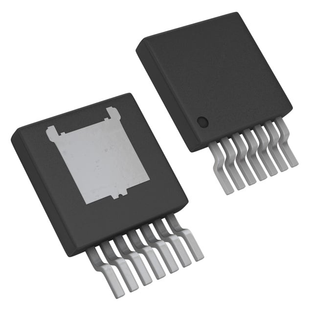
| 描述 | IC REG BUCK ADJ 5A TO263-7稳压器—开关式稳压器 5A SD Vtg Reg. |
| 产品分类 | |
| 品牌 | Texas Instruments |
| 产品手册 | http://www.ti.com/litv/snvs582m |
| 产品图片 |
|
| rohs | 符合RoHS无铅 / 符合限制有害物质指令(RoHS)规范要求 |
| 产品系列 | 电源管理 IC,稳压器—开关式稳压器,Texas Instruments LM22677TJ-ADJ/NOPBSIMPLE SWITCHER® |
| 数据手册 | |
| 产品型号 | LM22677TJ-ADJ/NOPB |
| PCN组件/产地 | |
| PWM类型 | 电压模式 |
| 产品培训模块 | http://www.digikey.cn/PTM/IndividualPTM.page?site=cn&lang=zhs&ptm=30128http://www.digikey.cn/PTM/IndividualPTM.page?site=cn&lang=zhs&ptm=30134 |
| 产品种类 | 稳压器—开关式稳压器 |
| 供应商器件封装 | TO-263-7 薄型 |
| 其它名称 | LM22677TJ-ADJ |
| 制造商产品页 | http://www.ti.com/general/docs/suppproductinfo.tsp?distId=10&orderablePartNumber=LM22677TJ-ADJ/NOPB |
| 包装 | 带卷 (TR) |
| 参考设计库 | http://www.digikey.com/rdl/4294959904/4294959903/316 |
| 同步整流器 | 无 |
| 商标 | Texas Instruments |
| 商标名 | SIMPLE SWITCHER |
| 安装类型 | 表面贴装 |
| 安装风格 | SMD/SMT |
| 封装 | Reel |
| 封装/外壳 | TO-263-7 薄型 |
| 封装/箱体 | TO-263-7 |
| 工作温度 | -40°C ~ 125°C |
| 工厂包装数量 | 1000 |
| 开关频率 | 500 kHz |
| 拓扑结构 | Buck |
| 最大工作温度 | + 125 C |
| 最大输入电压 | 42 V |
| 最小工作温度 | - 40 C |
| 最小输入电压 | 4.5 V |
| 标准包装 | 1,000 |
| 电压-输入 | 4.5 V ~ 42 V |
| 电压-输出 | 1.285 V ~ 37 V |
| 电流-输出 | 5A |
| 电源电压-最小 | 4.5 V |
| 类型 | Step Down |
| 系列 | LM22677 |
| 设计资源 | http://www.digikey.com/product-highlights/cn/zh/texas-instruments-webench-design-center/3176 |
| 负载调节 | 90 % |
| 输出数 | 1 |
| 输出电压 | Adj |
| 输出电流 | 5 A |
| 输出端数量 | 1 Output |
| 输出类型 | 可调式 |
| 配用 | /product-detail/zh/551600233-001%2FNOPB/551600233-001%2FNOPB-ND/1957528/product-detail/zh/LM22677EVAL%2FNOPB/LM22677EVAL%2FNOPB-ND/1955489 |
| 频率-开关 | 500kHz |


- 商务部:美国ITC正式对集成电路等产品启动337调查
- 曝三星4nm工艺存在良率问题 高通将骁龙8 Gen1或转产台积电
- 太阳诱电将投资9.5亿元在常州建新厂生产MLCC 预计2023年完工
- 英特尔发布欧洲新工厂建设计划 深化IDM 2.0 战略
- 台积电先进制程称霸业界 有大客户加持明年业绩稳了
- 达到5530亿美元!SIA预计今年全球半导体销售额将创下新高
- 英特尔拟将自动驾驶子公司Mobileye上市 估值或超500亿美元
- 三星加码芯片和SET,合并消费电子和移动部门,撤换高东真等 CEO
- 三星电子宣布重大人事变动 还合并消费电子和移动部门
- 海关总署:前11个月进口集成电路产品价值2.52万亿元 增长14.8%


PDF Datasheet 数据手册内容提取
Product Sample & Technical Tools & Support & Reference Folder Buy Documents Software Community Design LM22677,LM22677-Q1 SNVS582O–SEPTEMBER2008–REVISEDAUGUST2015 ® LM22677/-Q1 42-V, 5-A SIMPLE SWITCHER , Step-Down Voltage Regulator With Features 1 Features 3 Description • WideInputVoltageRange:4.5Vto42V The LM22677 switching regulator provides all of the 1 functions necessary to implement an efficient high- • InternallyCompensatedVoltageModeControl voltage step-down (buck) regulator using a minimum • StableWithLowESRCeramicCapacitors of external components. This easy-to-use regulator • 100-mΩ N-ChannelMOSFET incorporates a 42-V N-channel MOSFET switch that can provide up to 5 A of load current. Excellent line • OutputVoltageOptions: and load regulation along with high efficiency (> 90%) – -ADJ(OutputsasLowas1.285V) are featured. Voltage mode control offers short – -5.0(OutputFixedto5V) minimum on-time, allowing the widest ratio between input and output voltages. Internal loop compensation • ±1.5%FeedbackReferenceAccuracy means that the user is free from the tedious task of • 500-kHzDefaultSwitchingFrequency calculating the loop compensation components. Fixed • AdjustableSwitchingFrequencyand 5-V output and adjustable output voltage options are Synchronization available. The default switching frequency is set at 500 kHz, thus allowing for small external components • –40°Cto+125°COperatingJunctionTemperature and good transient response. In addition, the Range frequency can be adjusted over a range of 200 kHz • PrecisionEnableInput to 1 MHz with a single external resistor. The internal • IntegratedBoot-StrapDiode oscillator can be synchronized to a system clock or to • IntegratedSoft-Start the oscillator of another regulator. A precision enable input allows simplification of regulator control and • FullyWEBENCH®Enabled system power sequencing. In shutdown mode the • LM22677-Q1isanAutomotive-GradeProduct regulator draws only 25 µA (typical). The LM22677 thatisAEC-Q100Grade1Qualified(–40°Cto also has built-in thermal shutdown, and current +125°COperatingJunctionTemperature) limitingtoprotectagainstaccidentaloverloads. • NDR(ExposedPad) The LM22677 device is a member of Texas Instruments' SIMPLE SWITCHER® family. The 2 Applications SIMPLESWITCHERconceptprovidesforaneasy-to- use complete design using a minimum number of • IndustrialControl external components and the TI WEBENCH design • TelecomandDatacomSystems tool. TI's WEBENCH tool includes features such as • EmbeddedSystems external component calculation, electrical simulation, thermal simulation, and Build-It boards for easy • ConversionsfromStandard24-V,12-Vand5-V design-in. InputRails DeviceInformation(1) SimplifiedApplicationSchematic PARTNUMBER PACKAGE BODYSIZE(NOM) VIN VIN FB LM22677 TO-263(7) 10.16mmx9.85mm LM22677-Q1 LM22677-ADJ BOOT VOUT (1) For all available packages, see the orderable addendum at RT/SYNC EN GNDSW theendofthedatasheet. 1 An IMPORTANT NOTICE at the end of this data sheet addresses availability, warranty, changes, use in safety-critical applications, intellectualpropertymattersandotherimportantdisclaimers.PRODUCTIONDATA.
LM22677,LM22677-Q1 SNVS582O–SEPTEMBER2008–REVISEDAUGUST2015 www.ti.com Table of Contents 1 Features.................................................................. 1 7.4 DeviceFunctionalModes........................................12 2 Applications........................................................... 1 8 ApplicationsandImplementation...................... 15 3 Description............................................................. 1 8.1 ApplicationInformation............................................15 4 RevisionHistory..................................................... 2 8.2 TypicalApplication..................................................16 5 PinConfigurationandFunctions......................... 3 9 PowerSupplyRecommendations...................... 19 6 Specifications......................................................... 4 10 Layout................................................................... 19 6.1 AbsoluteMaximumRatings......................................4 10.1 LayoutGuidelines.................................................19 6.2 ESDRatings:LM22677............................................4 10.2 LayoutExample....................................................20 6.3 ESDRatings:LM22677-Q1......................................4 10.3 ThermalConsiderations........................................21 6.4 RecommendedOperatingConditions.......................4 11 DeviceandDocumentationSupport................. 22 6.5 ThermalInformation..................................................4 11.1 DocumentationSupport........................................22 6.6 ElectricalCharacteristics...........................................5 11.2 RelatedLinks........................................................22 6.7 TypicalCharacteristics..............................................6 11.3 Trademarks...........................................................22 7 DetailedDescription.............................................. 8 11.4 ElectrostaticDischargeCaution............................22 7.1 Overview...................................................................8 11.5 Glossary................................................................22 7.2 FunctionalBlockDiagram.........................................8 12 Mechanical,Packaging,andOrderable Information........................................................... 22 7.3 FeatureDescription...................................................8 4 Revision History ChangesfromRevisionN(November2014)toRevisionO Page • ChangedthewordPintoInput............................................................................................................................................... 1 • ChangedtheQgradepartnumbercorrectedtoLM22677fromLM2677';addediconforReferenceDesigntotopnavs...1 • Changed"PFM"Packageto"NDR"Package ....................................................................................................................... 3 ChangesfromRevisionM(April2013)toRevisionN Page • AddedPinConfigurationandFunctionssection,HandlingRatingtable,FeatureDescriptionsection,Device FunctionalModes,ApplicationandImplementationsection,PowerSupplyRecommendationssection,Layout section,DeviceandDocumentationSupportsection,andMechanical,Packaging,andOrderableInformation section ................................................................................................................................................................................... 1 • DeletedInvertingRegulatorApplication............................................................................................................................... 15 2 SubmitDocumentationFeedback Copyright©2008–2015,TexasInstrumentsIncorporated ProductFolderLinks:LM22677 LM22677-Q1
LM22677,LM22677-Q1 www.ti.com SNVS582O–SEPTEMBER2008–REVISEDAUGUST2015 5 Pin Configuration and Functions NDRPackage 7-PinTO-263 TopView 7 EN 6 FB 5 R T/SYNC 4 GND 3 BOOT 2 VIN 1 SW Exposed Pad Connect to GND PinFunctions PIN TYPE(1) DESCRIPTION APPLICATIONINFORMATION NAME NO. SW 1 O Switchoutput Switchingoutputofregulator VIN 2 I Inputvoltage Supplyinputtotheregulator BOOT 3 I Bootstrapinput ProvidesthegatevoltageforthehighsideN-FET Groundinputto GND 4 — regulator;system Systemgroundpin common Oscillatormodecontrol Usedtocontroloscillatormodeofregulator.SeeSwitchingFrequency RT/SYNC 5 I input AdjustmentandSynchronizationsectionofdatasheet. FB 6 I Feedbackinput Feedbackinputtoregulator Usedtocontrolregulatorstart-upandshutdown.SeePrecisionEnable EN 7 I Enableinput andUVLOsectionofdatasheet. Connecttoground.ProvidesthermalconnectiontoPCB.See EP EP — ExposedPad ApplicationsandImplementation. (1) O=Output,I=Input,G=Ground,P=Power Copyright©2008–2015,TexasInstrumentsIncorporated SubmitDocumentationFeedback 3 ProductFolderLinks:LM22677 LM22677-Q1
LM22677,LM22677-Q1 SNVS582O–SEPTEMBER2008–REVISEDAUGUST2015 www.ti.com 6 Specifications 6.1 Absolute Maximum Ratings(1)(2) MIN MAX UNIT VINtoGND 43 V ENPinVoltage –0.5 6 V RT/SYNCPinVoltage –0.5 7 V SWtoGND(3) –5 V V IN BOOTPinVoltage V +7 V SW FBPinVoltage –0.5 7 V PowerDissipation InternallyLimited JunctionTemperature 150 °C Forsolderingspecifications,refertoApplicationReportAbsoluteMaximumRatingsforSoldering(SNOA549). Storagetemperature,T –65 150 °C stg (1) AbsoluteMaximumRatingsindicatelimitsbeyondwhichdamagetothedevicemayoccur,includinginoperabilityanddegradationof devicereliabilityand/orperformance.Functionaloperationofthedeviceand/ornon-degradationattheabsolutemaximumratingsor otherconditionsbeyondthoseindicatedintheRecommendedOperatingConditionsisnotimplied.TheRecommendedOperating Conditionsindicateconditionsatwhichthedeviceisfunctionalandshouldnotbeoperatedbeyondsuchconditions. (2) IfMilitary/Aerospacespecifieddevicesarerequired,contacttheTexasInstrumentsSalesOffice/Distributorsforavailabilityand specifications. (3) Theabsolute-maximumspecificationofthe‘SWtoGND’appliestodcvoltage.Anextendednegativevoltagelimitof–10Vappliestoa pulseofupto50ns. 6.2 ESD Ratings: LM22677 VALUE UNIT V Electrostaticdischarge Human-bodymodel(HBM),perANSI/ESDA/JEDECJS-001(1) ±2000 V (ESD) (1) JEDECdocumentJEP155statesthat500-VHBMallowssafemanufacturingwithastandardESDcontrolprocess. 6.3 ESD Ratings: LM22677-Q1 VALUE UNIT V Electrostaticdischarge Human-bodymodel(HBM),perAECQ100-002(1) ±2000 V (ESD) (1) AECQ100-002indicatesthatHBMstressingshallbeinaccordancewiththeANSI/ESDA/JEDECJS-001specification. 6.4 Recommended Operating Conditions overoperatingfree-airtemperaturerange(unlessotherwisenoted) MIN MAX UNIT V SupplyVoltage 4.5 42 V IN JunctionTemperature –40 125 °C 6.5 Thermal Information LM22677 THERMALMETRIC(1)(2) NDR(TO-263) UNIT 7PINS R Junction-to-ambientthermalresistance 22 °C/W θJA (1) Formoreinformationabouttraditionalandnewthermalmetrics,seetheSemiconductorandICPackageThermalMetricsapplication report(SPRA953). (2) ThevalueofR fortheNDR(T)packageof22°C/Wisvalidifpackageismountedto1squareinchofcopper.TheR valuecan θJA J θJA rangefrom20to30°C/WdependingontheamountofPCBcopperdedicatedtoheattransfer.SeeapplicationnoteAN-1797TO-263 THINPackage(SNVA328)formoreinformation. 4 SubmitDocumentationFeedback Copyright©2008–2015,TexasInstrumentsIncorporated ProductFolderLinks:LM22677 LM22677-Q1
LM22677,LM22677-Q1 www.ti.com SNVS582O–SEPTEMBER2008–REVISEDAUGUST2015 6.6 Electrical Characteristics TypicalvaluesrepresentthemostlikelyparametricnormatT =T =25°C,andareprovidedforreferencepurposesonly. A J Unlessotherwisespecified:V =12V. IN PARAMETER TESTCONDITIONS MIN(1) TYP(2) MAX(1) UNIT LM22677-5.0 V =8Vto42V 4.925 5.0 5.075 IN V FeedbackVoltage V FB V =8Vto42V,–40°C≤T ≤125°C 4.9 5.1 IN J LM22677-ADJ V =4.7Vto42V 1.266 1.285 1.304 IN V FeedbackVoltage V FB V =4.7Vto42V,–40°C≤T ≤125°C 1.259 1.311 IN J ALLOUTPUTVOLTAGEVERSIONS V =5V 3.4 FB I QuiescentCurrent mA Q V =5V,–40°C≤T ≤125°C 6 FB J I StandbyQuiescentCurrent ENPin=0V 25 40 µA STDBY 6.0 7.1 8.4 I CurrentLimit A CL –40°C≤T ≤125°C 5.75 8.75 J V =42V,ENPin=0V,V =0V 0.2 2 µA IN SW I OutputLeakageCurrent L V =–1V 0.1 3 µA SW 0.1 0.14 R SwitchOn-Resistance Ω DS(ON) –40°C≤T ≤125°C 0.2 J 500 f OscillatorFrequency kHz O –40°C≤T ≤125°C 400 600 J 200 T MinimumOff-time ns OFFMIN –40°C≤T ≤125°C 100 300 J T MinimumOn-time 100 ns ONMIN I FeedbackBiasCurrent V =1.3V(ADJVersionOnly) 230 nA BIAS FB Falling 1.6 V EnableThresholdVoltage V EN Falling,–40°C≤T ≤125°C 1.3 1.9 J V EnableVoltageHysteresis 0.6 V ENHYST I EnableInputCurrent ENInput=0V 6 µA EN F MaximumSynchronizationFrequency V =3.5V,50%duty-cycle 1 MHz SYNC SYNC V SynchronizationThresholdVoltage 1.75 V SYNC T ThermalShutdownThreshold 150 °C SD (1) MINandMAXlimitsare100%productiontestedat25°C.Limitsovertheoperatingtemperaturerangeareensuredthroughcorrelation usingStatisticalQualityControl(SQC)methods.LimitsareusedtocalculateTI'sAverageOutgoingQualityLevel(AOQL). (2) Typicalvaluesrepresentmostlikelyparametricnormsattheconditionsspecifiedandarenotensured. Copyright©2008–2015,TexasInstrumentsIncorporated SubmitDocumentationFeedback 5 ProductFolderLinks:LM22677 LM22677-Q1
LM22677,LM22677-Q1 SNVS582O–SEPTEMBER2008–REVISEDAUGUST2015 www.ti.com 6.7 Typical Characteristics V =12V,T =25°C(unlessotherwisespecified). IN J Figure1.EfficiencyvsI andV ,V =3.3V Figure2.NormalizedSwitchingFrequencyvsTemperature OUT IN OUT Figure3.CurrentLimitvsTemperature Figure4.NormalizedRDS(ON)vsTemperature Figure5.FeedbackBiasCurrentvsTemperature Figure6.NormalizedEnableThresholdVoltagevs Temperature 6 SubmitDocumentationFeedback Copyright©2008–2015,TexasInstrumentsIncorporated ProductFolderLinks:LM22677 LM22677-Q1
LM22677,LM22677-Q1 www.ti.com SNVS582O–SEPTEMBER2008–REVISEDAUGUST2015 Typical Characteristics (continued) V =12V,T =25°C(unlessotherwisespecified). IN J Figure7.StandbyQuiescentCurrentvsInputVoltage Figure8.NormalizedFeedbackVoltagevsTemperature Figure9.NormalizedFeedbackVoltagevsInputVoltage Figure10.SwitchingFrequencyvsRT/SYNCResistor Copyright©2008–2015,TexasInstrumentsIncorporated SubmitDocumentationFeedback 7 ProductFolderLinks:LM22677 LM22677-Q1
LM22677,LM22677-Q1 SNVS582O–SEPTEMBER2008–REVISEDAUGUST2015 www.ti.com 7 Detailed Description 7.1 Overview The LM22677 device incorporates a voltage mode constant frequency PWM architecture. In addition, input voltage feedforward is used to stabilize the loop gain against variations in input voltage. This allows the loop compensation to be optimized for transient performance. The power MOSFET, in conjunction with the diode, produce a rectangular waveform at the switch pin, that swings from about zero volts to VIN. The inductor and output capacitor average this waveform to become the regulator output voltage. By adjusting the duty cycle of this waveform, the output voltage can be controlled. The error amplifier compares the output voltage with the internalreferenceandadjuststhedutycycletoregulatetheoutputatthedesiredvalue. The internal loop compensation of the -ADJ option is optimized for outputs of 5 V and below. If an output voltage of 5 V or greater is required, the -5.0 option can be used with an external voltage divider. The minimum output voltageisequaltothereferencevoltage,thatis,1.285V(typical). 7.2 Functional Block Diagram VIN VIN Vcc BOOT EN INTREG, EN,UVLO ILimit PWM Cmp. FB +- TCYOPME PIII +- LOGIC ErrorAmp. VOUT OSC SW 1.285V & Soft-Start RT/SYNC GND 7.3 Feature Description 7.3.1 PrecisionEnableandUVLO The precision enable input (EN) is used to control the regulator. The precision feature allows simple sequencing of multiple power supplies with a resistor divider from another supply. Connecting this pin to ground or to a voltagelessthan1.6V(typical)willturnofftheregulator.Thecurrentdrainfromtheinputsupply,inthisstate,is 25 µA (typical) at an input voltage of 12 V. The EN input has an internal pullup of about 6 µA. Therefore this pin can be left floating or pulled to a voltage greater than 2.2 V (typical) to turn the regulator on. The hysteresis on this input is about 0.6 V (typical) above the 1.6 V (typical) threshold. When driving the enable input, the voltage mustneverexceedthe6Vabsolutemaximumspecificationforthispin. 8 SubmitDocumentationFeedback Copyright©2008–2015,TexasInstrumentsIncorporated ProductFolderLinks:LM22677 LM22677-Q1
LM22677,LM22677-Q1 www.ti.com SNVS582O–SEPTEMBER2008–REVISEDAUGUST2015 Feature Description (continued) Although an internal pullup is provided on the EN pin, it is good practice to pull the input high, when this feature is not used, especially in noisy environments. This can most easily be done by connecting a resistor between V IN and the EN pin. The resistor is required, because the internal zener diode, at the EN pin, will conduct for voltages above about 6 V. The current in this zener must be limited to less than 100 µA. A resistor of 470 kΩ will limit the current to a safe value for input voltages as high 42 V. Smaller values of resistor can be used at lower inputvoltages. The LM22677 also incorporates an input undervoltage lock-out (UVLO) feature. This prevents the regulator from turningonwhentheinputvoltageisnotgreatenoughtoproperlybiastheinternalcircuitry.Therisingthresholdis 4.3 V (typical) while the falling threshold is 3.9 V (typical). In some cases these thresholds may be too low to provide good system performance. The solution is to use the EN input as an external UVLO to disable the part when the input voltage falls below a lower boundary. This is often used to prevent excessive battery discharge or early turn-on during start-up. This method is also recommended to prevent abnormal device operation in applications where the input voltage falls below the minimum of 4.5 V. Figure 11 shows the connections to implement this method of UVLO. Equation 1 and Equation 2 can be used to determine the correct resistor values. (1) where • V istheinputvoltagewheretheregulatorshutsoff. off • V isthevoltagewheretheregulatorturnson. (2) on Due to the 6 µA pullup, the current in the divider should be much larger than this. A value of 20 kΩ, for R is a ENB good first choice. Also, a zener diode may be needed between the EN pin and ground, in order to comply with theabsolutemaximumratingsonthispin. Vin RENT EN RENB Figure11. ExternalUVLOConnections 7.3.2 Soft-Start The soft-start feature allows the regulator to gradually reach steady-state operation, thus reducing start-up stresses. The internal soft-start feature brings the output voltage up in about 500 µs. This time is fixed and can notbechanged.Soft-startisresetanytimethepartisshutdownorathermaloverloadeventoccurs. 7.3.3 SwitchingFrequencyAdjustmentandSynchronization The LM22677 will operate in three different modes, depending on the condition of the RT/SYNC pin. With the RT/SYNC pin floating, the regulator will switch at the internally set frequency of 500 kHz (typ). With a resistor in the range of 25 kΩ to 200 kΩ, connected from RT/SYNC to ground, the internal switching frequency can be adjusted from 1 MHz to 200 kHz. Figure 12 shows the typical curve for switching frequency versus the external resistance connected to the RT/SYNC pin. The accuracy of the switching frequency, in this mode, is slightly worse than that of the internal oscillator; about ±25% is to be expected. Finally, an external clock can be applied to the RT/SYNC pin to allow the regulator to synchronize to a system clock or another LM22677. The mode is set during start-up of the regulator. When the LM22677 is enabled, or after V is applied, a weak pullup is IN connected to the RT/SYNC pin and, after approximately 100 µs, the voltage on the pin is checked against a Copyright©2008–2015,TexasInstrumentsIncorporated SubmitDocumentationFeedback 9 ProductFolderLinks:LM22677 LM22677-Q1
LM22677,LM22677-Q1 SNVS582O–SEPTEMBER2008–REVISEDAUGUST2015 www.ti.com Feature Description (continued) threshold of about 0.8 V. With the RT/SYNC pin open, the voltage floats above this threshold, and the mode is set to run with the internal clock. With a frequency set resistor present, an internal reference holds the pin voltage at 0.8 V; the resulting current sets the mode to allow the resistor to control the clock frequency. If the external circuit forces the RT/SYNC pin to a voltage much greater or less than 0.8 V, the mode is set to allow externalsynchronization.ThemodeislatcheduntileithertheENortheinputsupplyiscycled. The choice of switching frequency is governed by several considerations. As an example, lower frequencies may be desirable to reduce switching losses or improve duty cycle limits. Higher frequencies, or a specific frequency, may be desirable to avoid problems with EMI or reduce the physical size of external components. The flexibility of increasing the switching frequency above 500 kHz can also be used to operate outside a critical signal frequency band for a given application. Keep in mind that the values of inductor and output capacitor cannot be reduced dramatically, by operating above 500 kHz. This is true because the design of the internal loop compensationrestrictstherangeofthesecomponents. Frequency synchronization requires some care. First the external clock frequency must be greater than the internal clock frequency, and less than 1 MHz. The maximum internal switching frequency is specified in the ElectricalCharacteristicstable. NOTE The frequency adjust feature and the synchronization feature can not be used simultaneously. The synchronizing frequency must always be greater than the internal clock frequency. Secondly, the RT/SYNC pin must see a valid high or low voltage, during start-up, in order for the regulator to go into the synchronizing mode (see above). Also, the amplitude of the synchronizing pulses must comport with V levels found in the SYNC Electrical Characteristics table. The regulator will synchronize on the rising edge of the external clock. If the externalclockislostduringnormaloperation,theregulatorwillreverttothe500kHz(typical)internalclock. If the frequency synchronization feature is used, current limit foldback is not operational (see the Current Limit sectionfordetails). Figure12.SwitchingFrequencyvsRT/SYNCResistor 10 SubmitDocumentationFeedback Copyright©2008–2015,TexasInstrumentsIncorporated ProductFolderLinks:LM22677 LM22677-Q1
LM22677,LM22677-Q1 www.ti.com SNVS582O–SEPTEMBER2008–REVISEDAUGUST2015 Feature Description (continued) 7.3.4 SelfSynchronization It is possible to synchronize multiple LM22677 regulators together to share the same switching frequency. This can be done by tying the RT/SYNC pins together through a MOSFET and connecting a 1 kΩ resistor to ground at each pin. Figure 13 shows this connection. The gate of the MOSFET should be connected to the regulator with the highest output voltage. Also, the EN pins of both regulators should be tied to the common system enable, in order to properly initialize both regulators. The operation is as follows: When the regulators are enabled, the outputs are low and the MOSFET is off. The 1 kΩ resistors pull the RT/SYNC pins low, thus enabling the synchronization mode. These resistors are small enough to pull the RT/SYNC pin low, rather than activate the frequency adjust mode. Once the output voltage of one of the regulators is sufficient to turn on the MOSFET, the two RT/SYNC pins are tied together and the regulators will run in synchronization mode. The two regulators will be clocked at the same frequency but slightly phase shifted according to the minimum off-time of the regulator with the fastest internal oscillator. The slight phase shift helps to reduce stress on the input capacitors of the regulator. It is important to choose a MOSFET with a low gate threshold voltage so that the MOSFET will be fully enhanced. Also, a MOSFET with low inter-electrode capacitance is required. The 2N7002 isagoodchoice. ENABLE EN EN LM22677 LM22677 RT/SYNC RT/SYNC 2N7002 1 k(cid:13) 1 k(cid:13) Vout Figure13. SelfSynchronizingSetup 7.3.5 Boot-StrapSupply The LM22677 incorporates a floating high-side gate driver to control the power MOSFET. The supply for this driver is the external boot-strap capacitor connected between the BOOT pin and SW. A good quality 10 nF ceramic capacitor must be connected to these pins with short, wide PCB traces. One reason the regulator imposes a minimum off-time is to ensure that this capacitor recharges every switching cycle. A minimum load of about 5 mA is required to fully recharge the boot-strap capacitor in the minimum off-time. Some of this load can beprovidedbytheoutputvoltagedivider,ifused. 7.3.6 InternalCompensation The LM22677 has internal loop compensation designed to provide a stable regulator over a wide range of external power stage components. The internal compensation of the -ADJ option is optimized for output voltages below5V.Ifanoutputvoltageof5Vorgreaterisneeded,the-5.0optionwithanexternalresistordividercanbe used. Ensuring stability of a design with a specific power stage (inductor and output capacitor) can be tricky. The LM22677 stability can be verified using the WEBENCH Designer online circuit simulation tool. A quick start spreadsheetcanalsobedownloadedfromtheonlineproductfolder. The complete transfer function for the regulator loop is found by combining the compensation and power stage transfer functions. The LM22677 has internal type III loop compensation, as detailed in Figure 14. This is the approximate "straight line" function from the FB pin to the input of the PWM modulator. The power stage transfer function consists of a dc gain and a second order pole created by the inductor and output capacitor(s). Due to the input voltage feedforward employed in the LM22677, the power stage dc gain is fixed at 20 dB. The second order pole is characterized by its resonant frequency and its quality factor (Q). For a first pass design, the productofinductanceandoutputcapacitanceshouldconformtoEquation3. (3) Copyright©2008–2015,TexasInstrumentsIncorporated SubmitDocumentationFeedback 11 ProductFolderLinks:LM22677 LM22677-Q1
LM22677,LM22677-Q1 SNVS582O–SEPTEMBER2008–REVISEDAUGUST2015 www.ti.com Feature Description (continued) Alternatively,thispoleshouldbeplacedbetween1.5kHzand15kHzandisgivenbyEquation4. (4) The Q factor depends on the parasitic resistance of the power stage components and is not typically in the control of the designer. Of course, loop compensation is only one consideration when selecting power stage components(seetheApplicationsandImplementationsectionformoredetails). 40 -ADJ -5.0 35 B) N (d 30 AI G 25 R O 20 T A NS 15 E P M 10 O C 5 0 100 1k 10k 100k 1M 10M FREQUENCY (Hz) Figure14. CompensatorGain In general, hand calculations or simulations can only aid in selecting good power stage components. Good designpracticedictatesthatloadandlinetransienttestingshouldbedonetoverifythestabilityoftheapplication. Also, Bode plot measurements should be made to determine stability margins. AN-1889 How to Measure the Loop Transfer Function of Power Supplies (SNVA364) shows how to perform a loop transfer function measurementwithonlyanoscilloscopeandfunctiongenerator. 7.4 Device Functional Modes 7.4.1 CurrentLimit The LM22677 has current limiting to prevent the switch current from exceeding safe values during an accidental overloadontheoutput.ThispeakcurrentlimitisfoundintheElectricalCharacteristics tableundertheheadingof I . The maximum load current that can be provided, before current limit is reached, is determined from CL Equation5. where • Listhevalueofthepowerinductor. (5) When the LM22677 enters current limit, the output voltage will drop and the peak inductor current will be fixed at I at the end of each cycle. The switching frequency will remain constant while the duty cycle drops. The load CL currentwillnotremainconstant,butwilldependontheseverityoftheoverloadandtheoutputvoltage. For very severe overloads ("short-circuit"), the regulator changes to a low frequency current foldback mode of operation. The frequency foldback is about 1/5 of the nominal switching frequency. This will occur when the current limit trips before the minimum on-time has elapsed. This mode of operation is used to prevent inductor current "run-away", and is associated with very low output voltages when in overload. Equation 6 can be used to determinewhatlevelofoutputvoltagewillcausetheparttochangetolowfrequencycurrentfoldback. 12 SubmitDocumentationFeedback Copyright©2008–2015,TexasInstrumentsIncorporated ProductFolderLinks:LM22677 LM22677-Q1
LM22677,LM22677-Q1 www.ti.com SNVS582O–SEPTEMBER2008–REVISEDAUGUST2015 Device Functional Modes (continued) where • F isthenormalswitchingfrequency. sw • V isthemaximumfortheapplication. (6) in IftheoverloaddrivestheoutputvoltagetolessthanorequaltoV ,thedevicewillentercurrentfoldbackmode.If x a given application can drive the output voltage to ≤V , during an overload, then a second criterion must be x checked.Equation7givesthemaximuminputvoltage,wheninthismode,beforedamageoccurs: where • V isthevalueofoutputvoltageduringtheoverload. sc • F isthenormalswitchingfrequency. (7) sw NOTE If the input voltage should exceed this value while in foldback mode, the regulator and/or thediodemaybedamaged. It is important to note that the voltages in these equations are measured at the inductor. Normal trace and wiring resistance will cause the voltage at the inductor to be higher than that at a remote load. Therefore, even if the load is shorted with zero volts across its terminals, the inductor will still see a finite voltage. It is this value that should be used for V and V in the calculations. In order to return from foldback mode, the load must be x sc reduced to a value much lower than that required to initiate foldback. This load "hysteresis" is a normal aspect of anytypeofcurrentlimitfoldbackassociatedwithvoltageregulators. If the frequency synchronization feature is used, the current limit frequency fold-back is not operational, and the systemmaynotsurviveahardshort-circuitattheoutput. The safe operating areas, when in short circuit mode, are shown in Figure 15 through Figure 17, for different switchingfrequencies.Operatingpointsbelowandtotherightofthecurverepresentsafeoperation. NOTE Figure 15, Figure 16, and Figure 17 curves are not valid when the LM22677 is in frequencysynchronizationmode. 45 45 40 40 E (v) 35 E (v) 35 G 30 G 30 A A T SAFE OPERATING AREA T OL 25 OL 25 SAFE OPERATING AREA V V T 20 T 20 U U P P N 15 N 15 I I 10 10 5 5 0.0 0.2 0.4 0.6 0.8 1.0 1.2 0.0 0.2 0.4 0.6 0.8 1.0 1.2 SHORT CIRCUIT VOLTAGE (v) SHORT CIRCUIT VOLTAGE (v) Figure15.SOAat300kHz Figure16.SOAat500kHz Copyright©2008–2015,TexasInstrumentsIncorporated SubmitDocumentationFeedback 13 ProductFolderLinks:LM22677 LM22677-Q1
LM22677,LM22677-Q1 SNVS582O–SEPTEMBER2008–REVISEDAUGUST2015 www.ti.com Device Functional Modes (continued) 45 40 v) 35 E ( G 30 A T OL 25 V UT 20 SAFE OPERATING AREA P N 15 I 10 5 0.0 0.2 0.4 0.6 0.8 1.0 1.2 SHORT CIRCUIT VOLTAGE (v) Figure17.SOAat800kHz 7.4.2 ThermalProtection Internal thermal shutdown circuitry protects the LM22677 should the maximum junction temperature be exceeded. This protection is activated at about 150°C, with the result that the regulator will shut down until the temperaturedropsbelowabout135°C. 7.4.3 Duty-CycleLimits Ideally the regulator would control the duty cycle over the full range of zero to one. However, due to inherent delays in the circuitry, there are limits on both the maximum and minimum duty cycles that can be reliably controlled. This in turn places limits on the maximum and minimum input and output voltages that can be converted by the LM22677. A minimum on-time is imposed by the regulator in order to correctly measure the switch current during a current limit event. A minimum off-time is imposed in order the re-charge the bootstrap capacitor. Equation 8 can be used to determine the approximate maximum input voltage for a given output voltage. where • F istheswitchingfrequency. sw • T istheminimumon-time. (8) ON If the frequency adjust feature is used, that value should be used for F . Nominal values should be used. The sw worst case is lowest output voltage, and highest switching frequency. If this input voltage is exceeded, the regulator will skip cycles, effectively lowering the switching frequency. The consequences of this are higher outputvoltagerippleandadegradationoftheoutputvoltageaccuracy. Thesecondlimitationisthemaximumdutycyclebeforetheoutputvoltagewill"dropout"ofregulation.Equation9 canbeusedtoapproximatetheminimuminputvoltagebeforedropoutoccurs. where • ThevaluesofT andR arefoundintheElectricalCharacteristicstable. (9) OFF DS(ON) The worst case here is highest switching frequency and highest load. In Equation 9, R is the dc inductor L resistance.Ofcourse,thelowestinputvoltagetotheregulatormustnotbelessthan4.5V(typical). 14 SubmitDocumentationFeedback Copyright©2008–2015,TexasInstrumentsIncorporated ProductFolderLinks:LM22677 LM22677-Q1
LM22677,LM22677-Q1 www.ti.com SNVS582O–SEPTEMBER2008–REVISEDAUGUST2015 8 Applications and Implementation NOTE Information in the following applications sections is not part of the TI component specification, and TI does not warrant its accuracy or completeness. TI’s customers are responsible for determining suitability of components for their purposes. Customers should validateandtesttheirdesignimplementationtoconfirmsystemfunctionality. 8.1 Application Information The LM22677 is a step-down dc-to-dc regulator. It is typically used to convert a higher dc voltage to a lower dc voltage with a maximum output current of 5 A. The Detailed Design Procedure can be used to select componentsfortheLM22677.Alternately,theWEBENCHsoftwaremaybeusedtogeneratecompletedesigns. When generating a design, the WEBENCH software utilizes iterative design procedures and accesses comprehensivedatabasesofcomponents.GotoWEBENCHDesigner formoredetails. 8.1.1 OutputVoltageDividerSelection Foroutputvoltagesbetweenabout1.285Vand5V,the-ADJoptionshouldbeused,withanappropriatevoltage dividerasshowninFigure18.Equation10canbeusedtocalculatetheresistorvaluesofthisdivider: (10) A good value for R is 1 kΩ. This will help to provide some of the minimum load current requirement and FBB reduce susceptibility to noise pick-up. The top of R should be connected directly to the output capacitor or to FBT the load for remote sensing. If the divider is connected to the load, a local high-frequency bypass should be providedatthatlocation. For output voltages of 5 V, the -5.0 option should be used. In this case no divider is needed and the FB pin is connected to the output. The approximate values of the internal voltage divider are as follows: 7.38 kΩ from the FBpintotheinputoftheerroramplifierand2.55kΩfromtheretoground. Both the -ADJ and -5.0 options can be used for output voltages greater than 5 V, by using the correct output divider. As mentioned in the Internal Compensation section, the -5.0 option is optimized for output voltages of 5 V. However, for output voltages greater than 5 V, this option may provide better loop bandwidth than the -ADJ option, in some applications. If the -5.0 option is to be used at output voltages greater than 5 V, Equation11shouldbeusedtodeterminetheresistorvaluesintheoutputdivider. (11) AvalueofR ofabout1kΩ isagoodfirstchoice. FBB Vout RFBT FB RFBB Figure18. ResistiveFeedbackDivider A maximum value of 10 kΩ is recommended for the sum of R and R to maintain good output voltage FBB FBT accuracy for the -ADJ option. A maximum of 2 kΩ is recommended for the -5.0 option. For the -5.0 option, the totalinternaldividerresistanceistypically9.93kΩ. In all cases the output voltage divider should be placed as close as possible to the FB pin of the LM22677, becausethisisahighimpedanceinputandissusceptibletonoisepick-up. Copyright©2008–2015,TexasInstrumentsIncorporated SubmitDocumentationFeedback 15 ProductFolderLinks:LM22677 LM22677-Q1
LM22677,LM22677-Q1 SNVS582O–SEPTEMBER2008–REVISEDAUGUST2015 www.ti.com Application Information (continued) 8.1.2 PowerDiode A Schottky-type power diode is required for all LM22677 applications. Ultra-fast diodes are not recommended and may result in damage to the IC due to reverse recovery current transients. The near ideal reverse recovery characteristics and low forward voltage drop of Schottky diodes are particularly important for high input voltage and low output voltage applications common to the LM22677. The reverse breakdown rating of the diode should be selected for the maximum V , plus some safety margin. A good rule of thumb is to select a diode with a IN reversevoltageratingof1.3timesthemaximuminputvoltage. Select a diode with an average current rating at least equal to the maximum load current that will be seen in the application. 8.2 Typical Application Figure19showsanexampleofconvertinganinputvoltagerangeof5.5Vto42Vtoanoutputof3.3Vat5A. RFBB VIN 4.5V to 42V 976: VIN FB C3 EN LM22677-ADJ 10 nF EN BOOT L1 RFBT 1.54 k: 22 CPF2 + C6.18 PF C6.78 PFSYNC RT/SYNCGND SW 4.7 PH VOUT 3.3V D1 C4 + R3 60V, 5A 180 PF GND GND Figure19. TypicalBuckRegulatorApplication 8.2.1 DesignRequirements DESIGNPARAMETERS EXAMPLEVALUE DriverSupplyVoltage(V ) 4.5to42V IN OutputVoltage(V ) 3.3V OUT R CalculatedbasedonR andV of1.285V. FBT FBB REF R 1kΩto10kΩ FBB I 5A OUT 8.2.2 DetailedDesignProcedure 8.2.2.1 ExternalComponents Thefollowingguidelinesshouldbeusedwhendesigningastep-down(buck)converterwiththeLM22677. 8.2.2.2 Inductor The inductor value is determined based on the load current, ripple current, and the minimum and maximum input voltages. To keep the application in continuous conduction mode (CCM), the maximum ripple current, I , RIPPLE shouldbelessthantwicetheminimumloadcurrent. The general rule of keeping the inductor current peak-to-peak ripple around 30% of the nominal output current is a good compromise between excessive output voltage ripple and excessive component size and cost. Using this valueofripplecurrent,thevalueofinductor,L,iscalculatedusingEquation12. where 16 SubmitDocumentationFeedback Copyright©2008–2015,TexasInstrumentsIncorporated ProductFolderLinks:LM22677 LM22677-Q1
LM22677,LM22677-Q1 www.ti.com SNVS582O–SEPTEMBER2008–REVISEDAUGUST2015 • F istheswitchingfrequency. sw • V shouldbetakenatitsmaximumvalue,forthegivenapplication. (12) in The formula in Equation 12 provides a guide to select the value of the inductor L; the nearest standard value will thenbeusedinthecircuit. Oncetheinductorisselected,theactualripplecurrentcanbefoundfromEquation13. (13) Increasing the inductance will generally slow down the transient response but reduce the output voltage ripple. Reducingtheinductancewillgenerallyimprovethetransientresponsebutincreasetheoutputvoltageripple. The inductor must be rated for the peak current, I , in a given application, to prevent saturation. During normal PK loadingconditions,thepeakcurrentisequaltotheloadcurrentplus1/2oftheinductorripplecurrent. During an overload condition, as well as during certain load transients, the controller may trip current limit. In this case the peak inductor current is given by I , found in the Electrical Characteristics table. Good design practice CL requiresthattheinductorratingbeadequateforthisoverloadcondition. NOTE If the inductor is not rated for the maximum expected current, it can saturate resulting in damagetotheLM22677and/orthepowerdiode. 8.2.2.3 InputCapacitor The input capacitor selection is based on both input voltage ripple and RMS current. Good quality input capacitors are necessary to limit the ripple voltage at the VIN pin while supplying most of the regulator current during switch on-time. Low ESR ceramic capacitors are preferred. Larger values of input capacitance are desirable to reduce voltage ripple and noise on the input supply. This noise may find its way into other circuitry, sharing the same input supply, unless adequate bypassing is provided. A very approximate formula for determiningtheinputvoltagerippleisshowninEquation14. where • V isthepeak-to-peakripplevoltageattheswitchingfrequency. (14) ri Another concern is the RMS current passing through this capacitor. Equation 15 gives an approximation to this current. (15) ThecapacitormustberatedforatleastthislevelofRMScurrentattheswitchingfrequency. All ceramic capacitors have large voltage coefficients, in addition to normal tolerances and temperature coefficients. To help mitigate these effects, multiple capacitors can be used in parallel to bring the minimum capacitance up to the desired value. This may also help with RMS current constraints by sharing the current among several capacitors. Many times it is desirable to use an electrolytic capacitor on the input, in parallel with the ceramics. The moderate ESR of this capacitor can help to damp any ringing on the input supply caused by long power leads. This method can also help to reduce voltage spikes that may exceed the maximum input voltageratingoftheLM22677. It is good practice to include a high frequency bypass capacitor as close as possible to the LM22677. This small case size, low ESR, ceramic capacitor should be connected directly to the VIN and GND pins with the shortest possible PCB traces. Values in the range of 0.47 µF to 1 µF are appropriate. This capacitor helps to provide a low impedance supply to sensitive internal circuitry. It also helps to suppress any fast noise spikes on the input supplythatmayleadtoincreasedEMI. Copyright©2008–2015,TexasInstrumentsIncorporated SubmitDocumentationFeedback 17 ProductFolderLinks:LM22677 LM22677-Q1
LM22677,LM22677-Q1 SNVS582O–SEPTEMBER2008–REVISEDAUGUST2015 www.ti.com 8.2.2.4 OutputCapacitor The output capacitor is responsible for filtering the output voltage and supplying load current during transients. Capacitor selection depends on application conditions as well as ripple and transient requirements. Best performance is achieved with a parallel combination of ceramic capacitors and a low ESR SP™ or POSCAP™ type. Very low ESR capacitors such as ceramics reduce the output ripple and noise spikes, while higher value electrolytics or polymers provide large bulk capacitance to supply transients. Assuming very low ESR, Equation16givesanapproximationtotheoutputvoltageripple: (16) Typically,atotalvalueof100µForgreaterisrecommendedforoutputcapacitance. In applications with V less than 3.3 V, it is critical that low ESR output capacitors are selected. This will limit out potentialoutputvoltageovershootsastheinputvoltagefallsbelowthedevicenormaloperatingrange. If the switching frequency is set higher than 500 kHz, the capacitance value may not be reduced proportionally due to stability requirements. The internal compensation is optimized for circuits with a 500 kHz switching frequency.SeetheInternalCompensationsectionformoredetails. 8.2.2.5 Boot-StrapCapacitor The bootstrap capacitor between the BOOT pin and the SW pin supplies the gate current to turn on the N- channel MOSFET. The recommended value of this capacitor is 10 nF and should be a good quality, low ESR ceramiccapacitor. In some cases it may be desirable to slow down the turn-on of the internal power MOSFET, in order to reduce EMI. This can be done by placing a small resistor in series with the C capacitor. Resistors in the range of 10 boot Ω to 50 Ω can be used. This technique should only be used when absolutely necessary, because it will increase switchinglossesandtherebyreduceefficiency. 8.2.3 ApplicationCurves Figure20.EfficiencyvsI andV ,V =3.3V Figure21.SwitchingFrequencyvsRT/SYNCResistor OUT IN OUT 18 SubmitDocumentationFeedback Copyright©2008–2015,TexasInstrumentsIncorporated ProductFolderLinks:LM22677 LM22677-Q1
LM22677,LM22677-Q1 www.ti.com SNVS582O–SEPTEMBER2008–REVISEDAUGUST2015 9 Power Supply Recommendations The LM22677 is designed to operate from an input voltage supply range between 4.5 V and 42 V. This input supply should be able to withstand the maximum input current and maintain a voltage above 4.5 V. The resistance of the input supply rail should be low enough that an input current transient does not cause a high enoughdropattheLM22677supplyvoltagethatcancauseafalseUVLOfaulttriggeringandsystemreset. If the input supply is located more than a few inches from the LM22677 additional bulk capacitance may be required in addition to the ceramic bypass capacitors. The amount of bulk capacitance is not critical, but a 47 µF or100µFelectrolyticcapacitorisatypicalchoice. 10 Layout 10.1 Layout Guidelines Board layout is critical for the proper operation of switching power supplies. First, the ground plane area must be sufficient for thermal dissipation purposes. Second, appropriate guidelines must be followed to reduce the effects of switching noise. Switch mode converters are very fast switching devices. In such cases, the rapid increase of input current combined with the parasitic trace inductance generates unwanted L di/dt noise spikes. The magnitude of this noise tends to increase as the output current increases. This noise may turn into electromagneticinterference(EMI)andcanalsocauseproblemsindeviceperformance.Therefore,caremustbe takeninlayouttominimizetheeffectofthisswitchingnoise. The most important layout rule is to keep the ac current loops as small as possible. Figure 22 shows the current flowinabuckconverter.ThetopschematicshowsadottedlinewhichrepresentsthecurrentflowduringtheFET switchon-state.ThemiddleschematicshowsthecurrentflowduringtheFETswitchoff-state. The bottom schematic shows the currents referred to as ac currents. These ac currents are the most critical becausetheyarechanginginaveryshorttimeperiod.Thedottedlinesofthebottomschematicarethetracesto keep as short and wide as possible. This will also yield a small loop area reducing the loop inductance. To avoid functional problems due to layout, review the PCB layout example. Best results are achieved if the placement of the LM22677, the bypass capacitor, the Schottky diode, R , R and the inductor are placed as shown in the FBB FBT example. Note that, in the layout shown, R1 = R and R2 = R . It is also recommended to use 2-oz copper FBB FBT boards or heavier to help thermal dissipation and to reduce the parasitic inductances of board traces. See applicationnoteAN-1229SIMPLESWITCHER ® PCBLayoutGuidelines (SNVA054)formoreinformation. Figure22. CurrentFlowinaBuckApplication Copyright©2008–2015,TexasInstrumentsIncorporated SubmitDocumentationFeedback 19 ProductFolderLinks:LM22677 LM22677-Q1
LM22677,LM22677-Q1 SNVS582O–SEPTEMBER2008–REVISEDAUGUST2015 www.ti.com 10.2 Layout Example Figure23.PCBLayoutExample 20 SubmitDocumentationFeedback Copyright©2008–2015,TexasInstrumentsIncorporated ProductFolderLinks:LM22677 LM22677-Q1
LM22677,LM22677-Q1 www.ti.com SNVS582O–SEPTEMBER2008–REVISEDAUGUST2015 10.3 Thermal Considerations The components with the highest power dissipation are the power diode and the power MOSFET internal to the LM22677 regulator. The easiest method to determine the power dissipation within the LM22677 is to measure the total conversion losses then subtract the power losses in the diode and inductor. The total conversion loss is the difference between the input power and the output power. An approximation for the power diode loss is in Equation17. where • V isthediodevoltagedrop. (17) D AnapproximationfortheinductorpowerisshowninEquation18. where • R isthedcresistanceoftheinductor. L • The1.1factorisanapproximationfortheaclosses. (18) The regulator has an exposed thermal pad to aid power dissipation. Adding multiple vias under the device to the ground plane will greatly reduce the regulator junction temperature. Selecting a diode with an exposed pad will also aid the power dissipation of the diode. The most significant variables that affect the power dissipation of the regulator are output current, input voltage and operating frequency. The power dissipated while operating near the maximum output current and maximum input voltage can be appreciable. The junction-to-ambient thermal resistance of the LM22677 will vary with the application. The most significant variables are the area of copper in the PC board, the number of vias under the IC exposed pad and the amount of forced air cooling provided. A large continuos ground plane on the top of bottom PCB layer will provide the most effective heat dissipation. The integrity of the solder connection from the IC exposed pad to the PC board is critical. Excessive voids will greatly diminish the thermal dissipation capacity. The junction-to-ambient thermal resistance of the LM22677 NDR package is specified in the Electrical Characteristics table. See AN-2020 Thermal Design By Insight, Not Hindsight(SNVA419)formoreinformation. Copyright©2008–2015,TexasInstrumentsIncorporated SubmitDocumentationFeedback 21 ProductFolderLinks:LM22677 LM22677-Q1
LM22677,LM22677-Q1 SNVS582O–SEPTEMBER2008–REVISEDAUGUST2015 www.ti.com 11 Device and Documentation Support 11.1 Documentation Support 11.1.1 RelatedDocumentation • AN-1889HowtoMeasuretheLoopTransferFunctionofPowerSupplies (SNVA364) • AN-1892LM22677EvaluationBoard (SNVA366) • AN-1229SIMPLESWITCHER ® PCBLayoutGuidelines (SNVA054) • AN-2020ThermalDesignByInsight,NotHindsight (SNVA419) 11.2 Related Links The table below lists quick access links. Categories include technical documents, support and community resources,toolsandsoftware,andquickaccesstosampleorbuy. Table1.RelatedLinks TECHNICAL TOOLS& SUPPORT& PARTS PRODUCTFOLDER SAMPLE&BUY DOCUMENTS SOFTWARE COMMUNITY LM22677 Clickhere Clickhere Clickhere Clickhere Clickhere LM22677-Q1 Clickhere Clickhere Clickhere Clickhere Clickhere 11.3 Trademarks SIMPLESWITCHER,WEBENCHareregisteredtrademarksofTexasInstruments. Allothertrademarksarethepropertyoftheirrespectiveowners. 11.4 Electrostatic Discharge Caution Thesedeviceshavelimitedbuilt-inESDprotection.Theleadsshouldbeshortedtogetherorthedeviceplacedinconductivefoam duringstorageorhandlingtopreventelectrostaticdamagetotheMOSgates. 11.5 Glossary SLYZ022—TIGlossary. Thisglossarylistsandexplainsterms,acronyms,anddefinitions. 12 Mechanical, Packaging, and Orderable Information The following pages include mechanical, packaging, and orderable information. This information is the most current data available for the designated devices. This data is subject to change without notice and revision of thisdocument.Forbrowser-basedversionsofthisdatasheet,refertotheleft-handnavigation. 22 SubmitDocumentationFeedback Copyright©2008–2015,TexasInstrumentsIncorporated ProductFolderLinks:LM22677 LM22677-Q1
PACKAGE OPTION ADDENDUM www.ti.com 8-Oct-2015 PACKAGING INFORMATION Orderable Device Status Package Type Package Pins Package Eco Plan Lead/Ball Finish MSL Peak Temp Op Temp (°C) Device Marking Samples (1) Drawing Qty (2) (6) (3) (4/5) LM22677QTJ-ADJ/NOPB ACTIVE TO-263 NDR 7 1000 Green (RoHS CU SN Level-1-260C-UNLIM -40 to 125 LM22677 & no Sb/Br) QTJ-ADJ LM22677QTJE-5.0/NOPB ACTIVE TO-263 NDR 7 250 Green (RoHS CU SN Level-1-260C-UNLIM -40 to 125 LM22677 & no Sb/Br) QTJ-5.0 LM22677QTJE-ADJ/NOPB ACTIVE TO-263 NDR 7 250 Green (RoHS CU SN Level-1-260C-UNLIM -40 to 125 LM22677 & no Sb/Br) QTJ-ADJ LM22677TJ-5.0/NOPB ACTIVE TO-263 NDR 7 1000 Green (RoHS CU SN Level-1-260C-UNLIM -40 to 125 LM22677 & no Sb/Br) TJ-5.0 LM22677TJ-ADJ/NOPB ACTIVE TO-263 NDR 7 1000 Green (RoHS CU SN Level-1-260C-UNLIM -40 to 125 LM22677 & no Sb/Br) TJ-ADJ LM22677TJE-5.0/NOPB ACTIVE TO-263 NDR 7 250 Green (RoHS CU SN Level-1-260C-UNLIM -40 to 125 LM22677 & no Sb/Br) TJ-5.0 LM22677TJE-ADJ/NOPB ACTIVE TO-263 NDR 7 250 Green (RoHS CU SN Level-1-260C-UNLIM -40 to 125 LM22677 & no Sb/Br) TJ-ADJ (1) The marketing status values are defined as follows: ACTIVE: Product device recommended for new designs. LIFEBUY: TI has announced that the device will be discontinued, and a lifetime-buy period is in effect. NRND: Not recommended for new designs. Device is in production to support existing customers, but TI does not recommend using this part in a new design. PREVIEW: Device has been announced but is not in production. Samples may or may not be available. OBSOLETE: TI has discontinued the production of the device. (2) Eco Plan - The planned eco-friendly classification: Pb-Free (RoHS), Pb-Free (RoHS Exempt), or Green (RoHS & no Sb/Br) - please check http://www.ti.com/productcontent for the latest availability information and additional product content details. TBD: The Pb-Free/Green conversion plan has not been defined. Pb-Free (RoHS): TI's terms "Lead-Free" or "Pb-Free" mean semiconductor products that are compatible with the current RoHS requirements for all 6 substances, including the requirement that lead not exceed 0.1% by weight in homogeneous materials. Where designed to be soldered at high temperatures, TI Pb-Free products are suitable for use in specified lead-free processes. Pb-Free (RoHS Exempt): This component has a RoHS exemption for either 1) lead-based flip-chip solder bumps used between the die and package, or 2) lead-based die adhesive used between the die and leadframe. The component is otherwise considered Pb-Free (RoHS compatible) as defined above. Green (RoHS & no Sb/Br): TI defines "Green" to mean Pb-Free (RoHS compatible), and free of Bromine (Br) and Antimony (Sb) based flame retardants (Br or Sb do not exceed 0.1% by weight in homogeneous material) (3) MSL, Peak Temp. - The Moisture Sensitivity Level rating according to the JEDEC industry standard classifications, and peak solder temperature. (4) There may be additional marking, which relates to the logo, the lot trace code information, or the environmental category on the device. Addendum-Page 1
PACKAGE OPTION ADDENDUM www.ti.com 8-Oct-2015 (5) Multiple Device Markings will be inside parentheses. Only one Device Marking contained in parentheses and separated by a "~" will appear on a device. If a line is indented then it is a continuation of the previous line and the two combined represent the entire Device Marking for that device. (6) Lead/Ball Finish - Orderable Devices may have multiple material finish options. Finish options are separated by a vertical ruled line. Lead/Ball Finish values may wrap to two lines if the finish value exceeds the maximum column width. Important Information and Disclaimer:The information provided on this page represents TI's knowledge and belief as of the date that it is provided. TI bases its knowledge and belief on information provided by third parties, and makes no representation or warranty as to the accuracy of such information. Efforts are underway to better integrate information from third parties. TI has taken and continues to take reasonable steps to provide representative and accurate information but may not have conducted destructive testing or chemical analysis on incoming materials and chemicals. TI and TI suppliers consider certain information to be proprietary, and thus CAS numbers and other limited information may not be available for release. In no event shall TI's liability arising out of such information exceed the total purchase price of the TI part(s) at issue in this document sold by TI to Customer on an annual basis. OTHER QUALIFIED VERSIONS OF LM22677, LM22677-Q1 : •Catalog: LM22677 •Automotive: LM22677-Q1 NOTE: Qualified Version Definitions: •Catalog - TI's standard catalog product •Automotive - Q100 devices qualified for high-reliability automotive applications targeting zero defects Addendum-Page 2
PACKAGE MATERIALS INFORMATION www.ti.com 2-Sep-2015 TAPE AND REEL INFORMATION *Alldimensionsarenominal Device Package Package Pins SPQ Reel Reel A0 B0 K0 P1 W Pin1 Type Drawing Diameter Width (mm) (mm) (mm) (mm) (mm) Quadrant (mm) W1(mm) LM22677QTJ-ADJ/NOPB TO-263 NDR 7 1000 330.0 24.4 10.6 15.4 2.45 12.0 24.0 Q2 LM22677QTJE-5.0/NOPB TO-263 NDR 7 250 178.0 24.4 10.6 15.4 2.45 12.0 24.0 Q2 LM22677QTJE-ADJ/NOP TO-263 NDR 7 250 178.0 24.4 10.6 15.4 2.45 12.0 24.0 Q2 B LM22677TJ-5.0/NOPB TO-263 NDR 7 1000 330.0 24.4 10.6 15.4 2.45 12.0 24.0 Q2 LM22677TJ-ADJ/NOPB TO-263 NDR 7 1000 330.0 24.4 10.6 15.4 2.45 12.0 24.0 Q2 LM22677TJE-5.0/NOPB TO-263 NDR 7 250 178.0 24.4 10.6 15.4 2.45 12.0 24.0 Q2 LM22677TJE-ADJ/NOPB TO-263 NDR 7 250 178.0 24.4 10.6 15.4 2.45 12.0 24.0 Q2 PackMaterials-Page1
PACKAGE MATERIALS INFORMATION www.ti.com 2-Sep-2015 *Alldimensionsarenominal Device PackageType PackageDrawing Pins SPQ Length(mm) Width(mm) Height(mm) LM22677QTJ-ADJ/NOPB TO-263 NDR 7 1000 367.0 367.0 35.0 LM22677QTJE-5.0/NOPB TO-263 NDR 7 250 210.0 185.0 35.0 LM22677QTJE-ADJ/NOPB TO-263 NDR 7 250 210.0 185.0 35.0 LM22677TJ-5.0/NOPB TO-263 NDR 7 1000 367.0 367.0 35.0 LM22677TJ-ADJ/NOPB TO-263 NDR 7 1000 367.0 367.0 35.0 LM22677TJE-5.0/NOPB TO-263 NDR 7 250 210.0 185.0 35.0 LM22677TJE-ADJ/NOPB TO-263 NDR 7 250 210.0 185.0 35.0 PackMaterials-Page2
PACKAGE OUTLINE NDR0007A TO-263 - 2.25 mm max height SCALE 1.000 TO-263 10.1 0.735 A 7X 0.635 9.6 B 0.25 C A B PIN 1 ID 1 10.41 7.62 9.91 7 6X 1.27 14.36 13.66 12.45 11.95 R0.7 10.76 2.1 MAX TYP 10.26 1.9 0.508 7X C 0.381 0.15 7 1.05 0 -6 0-0.15 ALL AROUND 0.95 STAND-OFF NOTE 5 7.1 6.5 6.11 5.85 EXPOSED PAD (OUTLINE DOES NOT INCLUDE MOLD FLASH) 5.75 4.1 6.6 5.40 3.9 6.3 1.05 0.65 6.5 (2.66) 6.1 4219872/A 04/2019 NOTES: 1. All linear dimensions are in millimeters. Any dimensions in parenthesis are for reference only. Dimensioning and tolerancing per ASME Y14.5M. 2. This drawing is subject to change without notice. 3. Features may not exist and shape may vary per different assembly sites. 4. Reference JEDEC registration TO-279B. 5. Under all conditions, leads must not be above Datum C www.ti.com
EXAMPLE BOARD LAYOUT NDR0007A TO-263 - 2.25 mm max height TO-263 7X (2.41) 1 (6.35) 7X (0.91) 6X (1.27) 8 SYMM (7.62) (5.59) 7 (8.28) (0.91) PKG 0.07 MAX 0.07 MIN ALL AROUND ALL AROUND EXPOSED METAL EXPOSED METAL SOLDER MASK METAL SOLDER MASK OPENING METAL UNDER OPENING SOLDER MASK NON SOLDER MASK SOLDER MASK DEFINED DEFINED SOLDER MASK DETAILS 4219872/A 04/2019 NOTES: (continued) 6. This package is designed to be soldered to a thermal pad on the board. For more information, see Texas Instruments literature numbers SLMA002(www.ti.com/lit/slm002) and SLMA004 (www.ti.com/lit/slma004). 7. Vias are optional depending on application, refer to device data sheet. It is recommended that vias under paste be filled, plugged or tented. www.ti.com
EXAMPLE STENCIL DESIGN NDR0007A TO-263 - 2.25 mm max height TO-263 7X (2.41) 7X (0.91) EXPOSED METAL 1 (1.2) TYP (0.29) TYP 6X (1.27) (1.33) TYP R(0.05) TYP (0.665) 8 SYMM (7.62) 20X (1.13) 20X (1) 7 (8.28) 0.91 PKG SOLDER PASTE EXAMPLE BASED ON 0.125 mm THICK STENCIL EXPOSED PAD 64% PRINTED SOLDER COVERAGE BY AREA SCALE:7X 4219872/A 04/2019 NOTES: (continued) 8. Laser cutting apertures with trapezoidal walls and rounded corners may offer better paste release. IPC-7525 may have alternate design recommendations. 9. Board assembly site may have different recommendations for stencil design. www.ti.com
IMPORTANTNOTICEANDDISCLAIMER TIPROVIDESTECHNICALANDRELIABILITYDATA(INCLUDINGDATASHEETS),DESIGNRESOURCES(INCLUDINGREFERENCE DESIGNS),APPLICATIONOROTHERDESIGNADVICE,WEBTOOLS,SAFETYINFORMATION,ANDOTHERRESOURCES“ASIS” ANDWITHALLFAULTS,ANDDISCLAIMSALLWARRANTIES,EXPRESSANDIMPLIED,INCLUDINGWITHOUTLIMITATIONANY IMPLIEDWARRANTIESOFMERCHANTABILITY,FITNESSFORAPARTICULARPURPOSEORNON-INFRINGEMENTOFTHIRD PARTYINTELLECTUALPROPERTYRIGHTS. TheseresourcesareintendedforskilleddevelopersdesigningwithTIproducts.Youaresolelyresponsiblefor(1)selectingtheappropriate TIproductsforyourapplication,(2)designing,validatingandtestingyourapplication,and(3)ensuringyourapplicationmeetsapplicable standards,andanyothersafety,security,orotherrequirements.Theseresourcesaresubjecttochangewithoutnotice.TIgrantsyou permissiontousetheseresourcesonlyfordevelopmentofanapplicationthatusestheTIproductsdescribedintheresource.Other reproductionanddisplayoftheseresourcesisprohibited.NolicenseisgrantedtoanyotherTIintellectualpropertyrightortoanythird partyintellectualpropertyright.TIdisclaimsresponsibilityfor,andyouwillfullyindemnifyTIanditsrepresentativesagainst,anyclaims, damages,costs,losses,andliabilitiesarisingoutofyouruseoftheseresources. TI’sproductsareprovidedsubjecttoTI’sTermsofSale(www.ti.com/legal/termsofsale.html)orotherapplicabletermsavailableeitheron ti.comorprovidedinconjunctionwithsuchTIproducts.TI’sprovisionoftheseresourcesdoesnotexpandorotherwisealterTI’sapplicable warrantiesorwarrantydisclaimersforTIproducts. MailingAddress:TexasInstruments,PostOfficeBox655303,Dallas,Texas75265 Copyright©2019,TexasInstrumentsIncorporated