ICGOO在线商城 > 集成电路(IC) > 嵌入式 - FPGA(现场可编程门阵列) > LFE3-150EA-8FN1156C
 Datasheet下载
- 型号: LFE3-150EA-8FN1156C
- 制造商: Lattice
- 库位|库存: xxxx|xxxx
- 要求:
| 数量阶梯 | 香港交货 | 国内含税 |
| +xxxx | $xxxx | ¥xxxx |
查看当月历史价格
查看今年历史价格
LFE3-150EA-8FN1156C产品简介:
ICGOO电子元器件商城为您提供LFE3-150EA-8FN1156C由Lattice设计生产,在icgoo商城现货销售,并且可以通过原厂、代理商等渠道进行代购。 LFE3-150EA-8FN1156C价格参考。LatticeLFE3-150EA-8FN1156C封装/规格:嵌入式 - FPGA(现场可编程门阵列), 。您可以下载LFE3-150EA-8FN1156C参考资料、Datasheet数据手册功能说明书,资料中有LFE3-150EA-8FN1156C 详细功能的应用电路图电压和使用方法及教程。
Lattice Semiconductor Corporation(莱迪思半导体公司)的LFE3-150EA-8FN1156C属于嵌入式FPGA(现场可编程门阵列),基于Lattice的ECP3系列。该型号具有低功耗、高性能和小尺寸的特点,适用于多种嵌入式系统应用场景。以下是其主要应用场景:

 1. 通信设备
   - 小型基站:用于无线通信中的信号处理、协议转换和数据传输。
   - 网络接口卡(NIC):实现高速数据包处理、流量管理和协议加速。
   - 背板通信:支持高带宽、低延迟的数据交换和信号桥接。

 2. 工业自动化
   - 实时控制:在工业控制系统中执行复杂的逻辑运算和实时数据处理。
   - 电机控制:通过FPGA实现高效、精确的PWM生成和反馈控制。
   - 传感器融合:整合多种传感器数据,提供更精准的环境感知能力。

 3. 汽车电子
   - ADAS(高级驾驶辅助系统):用于图像处理、传感器数据融合和算法加速。
   - 车载信息娱乐系统:实现音频/视频信号处理、显示控制和接口转换。
   - CAN总线桥接:支持不同通信协议之间的数据转换和同步。

 4. 消费电子
   - 高清视频处理:用于视频编码、解码和图像增强。
   - 显示接口转换:支持HDMI、MIPI、LVDS等多种显示接口的互连和转换。
   - 智能家居设备:实现物联网设备的信号处理和协议适配。

 5. 医疗设备
   - 医学影像处理:用于超声、CT等设备的图像采集和预处理。
   - 患者监护系统:实现多通道信号采集、处理和传输。
   - 便携式医疗设备:利用低功耗特性延长电池续航时间。

 6. 航空航天与国防
   - 雷达信号处理:用于目标检测、跟踪和信号分析。
   - 卫星通信:实现高可靠性的数据处理和协议转换。
   - 导航系统:支持复杂算法的硬件加速和实时计算。

 7. 边缘计算
   - AI推理加速:为边缘设备提供轻量级的人工智能推理能力。
   - 数据预处理:对传感器数据进行压缩、加密和格式转换。
   - 网络安全:实现数据加密、解密和安全协议加速。

LFE3-150EA-8FN1156C凭借其灵活的架构和丰富的I/O资源,能够满足多种嵌入式系统的特定需求,尤其适合对成本敏感、功耗要求低且性能适中的应用场合。
| 参数 | 数值 |
| 产品目录 | 集成电路 (IC) |
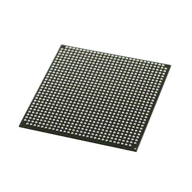
| 描述 | IC FPGA 586 I/O 1156BGA |
| 产品分类 | |
| I/O数 | 586 |
| LAB/CLB数 | 18625 |
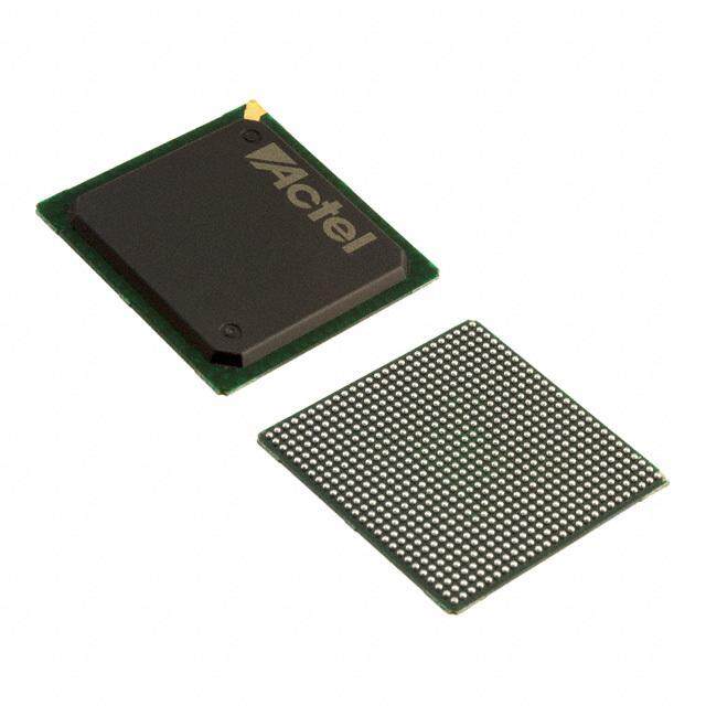
| 品牌 | Lattice Semiconductor Corporation |
| 数据手册 | |
| 产品图片 |
|
| 产品型号 | LFE3-150EA-8FN1156C |
| PCN组件/产地 | |
| PCN设计/规格 | http://www.latticesemi.com/~/media/Documents/ProductChangeNotification/13/PCN03A-13_Alternate_Qualified_Assembly_Test%20Site_Material_Sets_ASE_Taiwan.ashx |
| rohs | 无铅 / 符合限制有害物质指令(RoHS)规范要求 |
| 产品系列 | ECP3 |
| 产品培训模块 | http://www.digikey.cn/PTM/IndividualPTM.page?site=cn&lang=zhs&ptm=25717 |
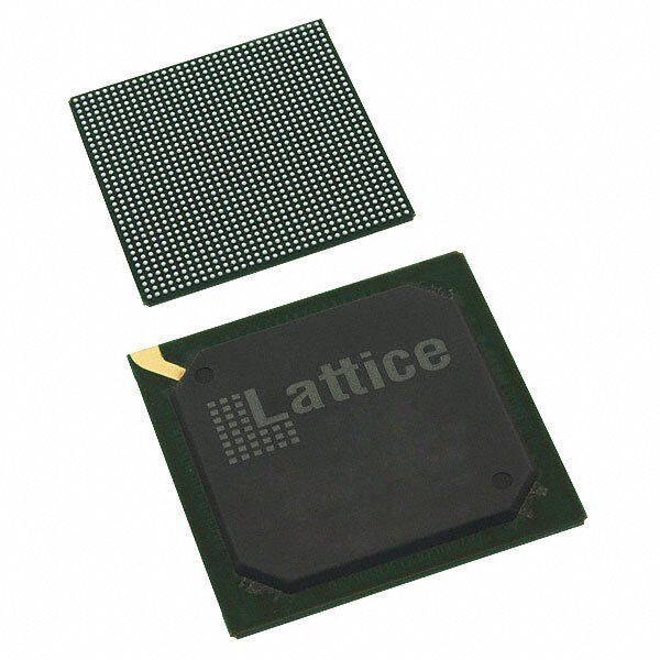
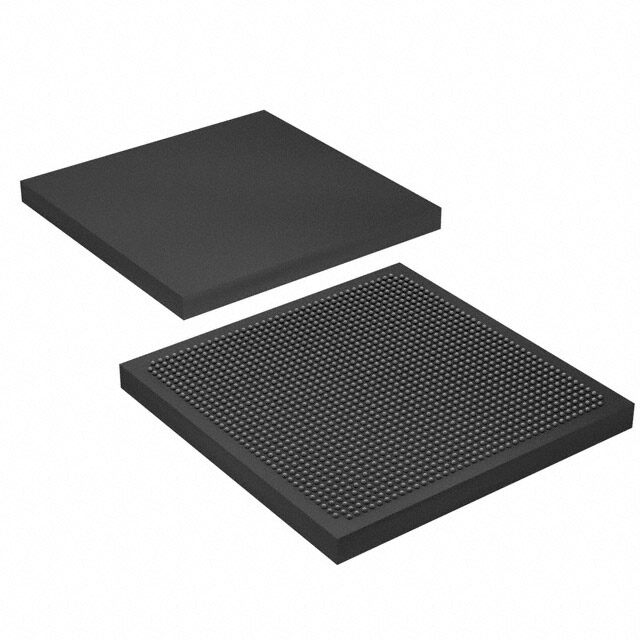
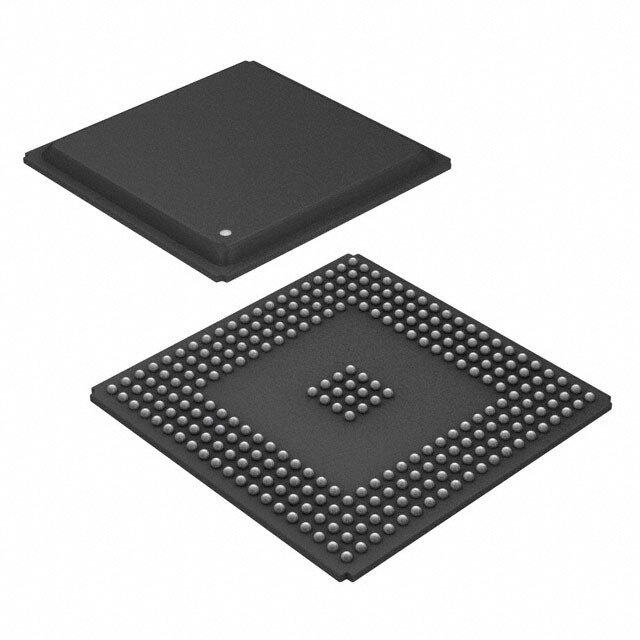
| 供应商器件封装 | 1156-FPBGA(35x35) |
| 其它名称 | 220-1162 |
| 安装类型 | 表面贴装 |
| 封装/外壳 | 1156-BBGA |
| 工作温度 | 0°C ~ 85°C |
| 总RAM位数 | 7014400 |
| 栅极数 | - |
| 标准包装 | 24 |
| 电压-电源 | 1.14 V ~ 1.26 V |
| 逻辑元件/单元数 | 149000 |


- 商务部:美国ITC正式对集成电路等产品启动337调查
- 曝三星4nm工艺存在良率问题 高通将骁龙8 Gen1或转产台积电
- 太阳诱电将投资9.5亿元在常州建新厂生产MLCC 预计2023年完工
- 英特尔发布欧洲新工厂建设计划 深化IDM 2.0 战略
- 台积电先进制程称霸业界 有大客户加持明年业绩稳了
- 达到5530亿美元!SIA预计今年全球半导体销售额将创下新高
- 英特尔拟将自动驾驶子公司Mobileye上市 估值或超500亿美元
- 三星加码芯片和SET,合并消费电子和移动部门,撤换高东真等 CEO
- 三星电子宣布重大人事变动 还合并消费电子和移动部门
- 海关总署:前11个月进口集成电路产品价值2.52万亿元 增长14.8%
PDF Datasheet 数据手册内容提取
LatticeECP3 Family Data Sheet DS1021 Version 02.8EA, March 2015
LatticeECP3 Family Data Sheet Introduction February 2012 Data Sheet DS1021 Features (cid:129) Dedicated read/write levelling functionality (cid:129) Dedicated gearing logic Higher Logic Density for Increased System (cid:129) Source synchronous standards support Integration —ADC/DAC, 7:1 LVDS, XGMII • 17K to 149K LUTs —High Speed ADC/DAC devices (cid:129) 116 to 586 I/Os (cid:129) Dedicated DDR/DDR2/DDR3 memory with DQS Embedded SERDES support (cid:129) 150 Mbps to 3.2 Gbps for Generic 8b10b, 10-bit (cid:129) Optional Inter-Symbol Interference (ISI) SERDES, and 8-bit SERDES modes correction on outputs (cid:129) Data Rates 230 Mbps to 3.2 Gbps per channel Programmable sysI/O™ Buffer Supports for all other protocols Wide Range of Interfaces (cid:129) Up to 16 channels per device: PCI Express, (cid:129) On-chip termination SONET/SDH, Ethernet (1GbE, SGMII, XAUI), (cid:129) Optional equalization filter on inputs CPRI, SMPTE 3G and Serial RapidIO (cid:129) LVTTL and LVCMOS 33/25/18/15/12 sysDSP™ (cid:129) SSTL 33/25/18/15 I, II (cid:129) Fully cascadable slice architecture (cid:129) HSTL15 I and HSTL18 I, II (cid:129) 12 to 160 slices for high performance multiply (cid:129) PCI and Differential HSTL, SSTL and accumulate (cid:129) LVDS, Bus-LVDS, LVPECL, RSDS, MLVDS (cid:129) Powerful 54-bit ALU operations Flexible Device Configuration (cid:129) Time Division Multiplexing MAC Sharing (cid:129) Dedicated bank for configuration I/Os (cid:129) Rounding and truncation (cid:129) SPI boot flash interface (cid:129) Each slice supports (cid:129) Dual-boot images supported —Half 36x36, two 18x18 or four 9x9 multipliers (cid:129) Slave SPI —Advanced 18x36 MAC and 18x18 Multiply- (cid:129) TransFR™ I/O for simple field updates Multiply-Accumulate (MMAC) operations (cid:129) Soft Error Detect embedded macro Flexible Memory Resources System Level Support (cid:129) Up to 6.85Mbits sysMEM™ Embedded Block (cid:129) IEEE 1149.1 and IEEE 1532 compliant RAM (EBR) (cid:129) Reveal Logic Analyzer (cid:129) 36K to 303K bits distributed RAM (cid:129) ORCAstra FPGA configuration utility sysCLOCK Analog PLLs and DLLs (cid:129) On-chip oscillator for initialization & general use (cid:129) Two DLLs and up to ten PLLs per device (cid:129) 1.2 V core power supply Pre-Engineered Source Synchronous I/O (cid:129) DDR registers in I/O cells Table 1-1. LatticeECP3™ Family Selection Guide Device ECP3-17 ECP3-35 ECP3-70 ECP3-95 ECP3-150 LUTs (K) 17 33 67 92 149 sysMEM Blocks (18 Kbits) 38 72 240 240 372 Embedded Memory (Kbits) 700 1327 4420 4420 6850 Distributed RAM Bits (Kbits) 36 68 145 188 303 18 x 18 Multipliers 24 64 128 128 320 SERDES (Quad) 1 1 3 3 4 PLLs/DLLs 2 / 2 4 / 2 10 / 2 10 / 2 10 / 2 Packages and SERDES Channels/ I/O Combinations 328 csBGA (10 x 10 mm) 2 / 116 256 ftBGA (17 x 17 mm) 4 / 133 4 / 133 484 fpBGA (23 x 23 mm) 4 / 222 4 / 295 4 / 295 4 / 295 672 fpBGA (27 x 27 mm) 4 / 310 8 / 380 8 / 380 8 / 380 1156 fpBGA (35 x 35 mm) 12 / 490 12 / 490 16 / 586 © 2012 Lattice Semiconductor Corp. All Lattice trademarks, registered trademarks, patents, and disclaimers are as listed at www.latticesemi.com/legal. All other brand or product names are trademarks or registered trademarks of their respective holders. The specifications and information herein are subject to change without notice. www.latticesemi.com 1-1 DS1021 Introduction_01.6
Introduction LatticeECP3 Family Data Sheet Introduction The LatticeECP3™ (EConomy Plus Third generation) family of FPGA devices is optimized to deliver high perfor- mance features such as an enhanced DSP architecture, high speed SERDES and high speed source synchronous interfaces in an economical FPGA fabric. This combination is achieved through advances in device architecture and the use of 65 nm technology making the devices suitable for high-volume, high-speed, low-cost applications. The LatticeECP3 device family expands look-up-table (LUT) capacity to 149K logic elements and supports up to 586 user I/Os. The LatticeECP3 device family also offers up to 320 18 x 18 multipliers and a wide range of parallel I/O standards. The LatticeECP3 FPGA fabric is optimized with high performance and low cost in mind. The LatticeECP3 devices utilize reconfigurable SRAM logic technology and provide popular building blocks such as LUT-based logic, distrib- uted and embedded memory, Phase Locked Loops (PLLs), Delay Locked Loops (DLLs), pre-engineered source synchronous I/O support, enhanced sysDSP slices and advanced configuration support, including encryption and dual-boot capabilities. The pre-engineered source synchronous logic implemented in the LatticeECP3 device family supports a broad range of interface standards, including DDR3, XGMII and 7:1 LVDS. The LatticeECP3 device family also features high speed SERDES with dedicated PCS functions. High jitter toler- ance and low transmit jitter allow the SERDES plus PCS blocks to be configured to support an array of popular data protocols including PCI Express, SMPTE, Ethernet (XAUI, GbE, and SGMII) and CPRI. Transmit Pre-empha- sis and Receive Equalization settings make the SERDES suitable for transmission and reception over various forms of media. The LatticeECP3 devices also provide flexible, reliable and secure configuration options, such as dual-boot capa- bility, bit-stream encryption, and TransFR field upgrade features. The Lattice Diamond™ and ispLEVER® design software allows large complex designs to be efficiently imple- mented using the LatticeECP3 FPGA family. Synthesis library support for LatticeECP3 is available for popular logic synthesis tools. Diamond and ispLEVER tools use the synthesis tool output along with the constraints from its floor planning tools to place and route the design in the LatticeECP3 device. The tools extract the timing from the routing and back-annotate it into the design for timing verification. Lattice provides many pre-engineered IP (Intellectual Property) modules for the LatticeECP3 family. By using these configurable soft core IPs as standardized blocks, designers are free to concentrate on the unique aspects of their design, increasing their productivity. 1-2
LatticeECP3 Family Data Sheet Architecture June 2013 Data Sheet DS1021 Architecture Overview Each LatticeECP3 device contains an array of logic blocks surrounded by Programmable I/O Cells (PIC). Inter- spersed between the rows of logic blocks are rows of sysMEM™ Embedded Block RAM (EBR) and rows of sys- DSP™ Digital Signal Processing slices, as shown in Figure 2-1. The LatticeECP3-150 has four rows of DSP slices; all other LatticeECP3 devices have two rows of DSP slices. In addition, the LatticeECP3 family contains SERDES Quads on the bottom of the device. There are two kinds of logic blocks, the Programmable Functional Unit (PFU) and Programmable Functional Unit without RAM (PFF). The PFU contains the building blocks for logic, arithmetic, RAM and ROM functions. The PFF block contains building blocks for logic, arithmetic and ROM functions. Both PFU and PFF blocks are optimized for flexibility, allowing complex designs to be implemented quickly and efficiently. Logic Blocks are arranged in a two- dimensional array. Only one type of block is used per row. The LatticeECP3 devices contain one or more rows of sysMEM EBR blocks. sysMEM EBRs are large, dedicated 18Kbit fast memory blocks. Each sysMEM block can be configured in a variety of depths and widths as RAM or ROM. In addition, LatticeECP3 devices contain up to two rows of DSP slices. Each DSP slice has multipliers and adder/accumulators, which are the building blocks for complex signal processing capabilities. The LatticeECP3 devices feature up to 16 embedded 3.2 Gbps SERDES (Serializer / Deserializer) channels. Each SERDES channel contains independent 8b/10b encoding / decoding, polarity adjust and elastic buffer logic. Each group of four SERDES channels, along with its Physical Coding Sub-layer (PCS) block, creates a quad. The func- tionality of the SERDES/PCS quads can be controlled by memory cells set during device configuration or by regis- ters that are addressable during device operation. The registers in every quad can be programmed via the SERDES Client Interface (SCI). These quads (up to four) are located at the bottom of the devices. Each PIC block encompasses two PIOs (PIO pairs) with their respective sysI/O buffers. The sysI/O buffers of the LatticeECP3 devices are arranged in seven banks, allowing the implementation of a wide variety of I/O standards. In addition, a separate I/O bank is provided for the programming interfaces. 50% of the PIO pairs on the left and right edges of the device can be configured as LVDS transmit/receive pairs. The PIC logic also includes pre-engi- neered support to aid in the implementation of high speed source synchronous standards such as XGMII, 7:1 LVDS, along with memory interfaces including DDR3. The LatticeECP3 registers in PFU and sysI/O can be configured to be SET or RESET. After power up and the device is configured, it enters into user mode with these registers SET/RESET according to the configuration set- ting, allowing the device entering to a known state for predictable system function. Other blocks provided include PLLs, DLLs and configuration functions. The LatticeECP3 architecture provides two Delay Locked Loops (DLLs) and up to ten Phase Locked Loops (PLLs). The PLL and DLL blocks are located at the end of the EBR/DSP rows. The configuration block that supports features such as configuration bit-stream decryption, transparent updates and dual-boot support is located toward the center of this EBR row. Every device in the LatticeECP3 family sup- ports a sysCONFIG™ port located in the corner between banks one and two, which allows for serial or parallel device configuration. In addition, every device in the family has a JTAG port. This family also provides an on-chip oscillator and soft error detect capability. The LatticeECP3 devices use 1.2 V as their core voltage. © 2013 Lattice Semiconductor Corp. All Lattice trademarks, registered trademarks, patents, and disclaimers are as listed at www.latticesemi.com/legal. All other brand or product names are trademarks or registered trademarks of their respective holders. The specifications and information herein are subject to change without notice. www.latticesemi.com 2-1 DS1021 Architecture_02.1
Architecture LatticeECP3 Family Data Sheet Figure 2-1. Simplified Block Diagram, LatticeECP3-35 Device (Top Level) sysIO sysIO Configuration Logic: Bank 0 Bank 1 Dual-boot, Encryption and Transparent Updates JTAG On-chip Oscillator Pre-engineered Source Synchronous Support: sysIO sysIO DDR3 - 800 Mbps Bank Bank Generic - Up to 1 Gbps 7 2 Enhanced DSP Slices: Multiply, Accumulate and ALU sysCLOCK PLLs & DLLs: Frequency Synthesis and Clock Alignment Flexible sysIO: LVCMOS, HSTL, SSTL, LVDS Up to 486 I/Os sysMEM Block RAM: 18 Kbit Flexible Routing: Optimized for speed and routability Programmable SERDES/PCS SERDES/PCS SERDES/PCS SERDES/PCS Function Units: CH 3 CH 2 CH 1 CH 0 Up to 149K LUTs sysIO Bank 6 sysIO Bank 3 3.2 Gbps SERDES Note: There is no Bank 4 or Bank 5 in LatticeECP3 devices. PFU Blocks The core of the LatticeECP3 device consists of PFU blocks, which are provided in two forms, the PFU and PFF. The PFUs can be programmed to perform Logic, Arithmetic, Distributed RAM and Distributed ROM functions. PFF blocks can be programmed to perform Logic, Arithmetic and ROM functions. Except where necessary, the remain- der of this data sheet will use the term PFU to refer to both PFU and PFF blocks. Each PFU block consists of four interconnected slices numbered 0-3 as shown in Figure 2-2. Each slice contains two LUTs. All the interconnections to and from PFU blocks are from routing. There are 50 inputs and 23 outputs associated with each PFU block. 2-2
Architecture LatticeECP3 Family Data Sheet Figure 2-2. PFU Diagram From Routing LUT4& LUT4& LUT4& LUT4& LUT4& LUT4& CARRY CARRY CARRY CARRY CARRY CARRY LUT4 LUT4 Slice 0 Slice 1 Slice 2 Slice 3 D D D D D D FF FF FF FF FF FF To Routing Slice Slice 0 through Slice 2 contain two LUT4s feeding two registers, whereas Slice 3 contains two LUT4s only. For PFUs, Slice 0 through Slice 2 can be configured as distributed memory, a capability not available in the PFF. Table 2-1 shows the capability of the slices in both PFF and PFU blocks along with the operation modes they enable. In addition, each PFU contains logic that allows the LUTs to be combined to perform functions such as LUT5, LUT6, LUT7 and LUT8. There is control logic to perform set/reset functions (programmable as synchronous/ asynchronous), clock select, chip-select and wider RAM/ROM functions. Table 2-1. Resources and Modes Available per Slice PFU BLock PFF Block Slice Resources Modes Resources Modes Slice 0 2 LUT4s and 2 Registers Logic, Ripple, RAM, ROM 2 LUT4s and 2 Registers Logic, Ripple, ROM Slice 1 2 LUT4s and 2 Registers Logic, Ripple, RAM, ROM 2 LUT4s and 2 Registers Logic, Ripple, ROM Slice 2 2 LUT4s and 2 Registers Logic, Ripple, RAM, ROM 2 LUT4s and 2 Registers Logic, Ripple, ROM Slice 3 2 LUT4s Logic, ROM 2 LUT4s Logic, ROM Figure 2-3 shows an overview of the internal logic of the slice. The registers in the slice can be configured for posi- tive/negative and edge triggered or level sensitive clocks. Slices 0, 1 and 2 have 14 input signals: 13 signals from routing and one from the carry-chain (from the adjacent slice or PFU). There are seven outputs: six to routing and one to carry-chain (to the adjacent PFU). Slice 3 has 10 input signals from routing and four signals to routing. Table 2-2 lists the signals associated with Slice 0 to Slice 2. 2-3
Architecture LatticeECP3 Family Data Sheet Figure 2-3. Slice Diagram FCO To Different Slice/PFU SLICE FXB OFX1 FXA A1 CO F1 B1 F/SUM C1 D1 LUT4 & D Q1 CARRY* FF* CI To Routing M1 M0 LUT5 From Mux Routing OFX0 A0 CO B0 C0 F0 D0 LUT4 & CARRY* F/SUM D Q0 FF* CI CE CLK LSR * Not in Slice 3 FCI From Different Slice/PFU For Slices 0 and 1, memory control signals are generated from Slice 2 as follows: WCK is CLK WRE is from LSR DI[3:2] for Slice 1 and DI[1:0] for Slice 0 data from Slice 2 WAD [A:D] is a 4-bit address from slice 2 LUT input Table 2-2. Slice Signal Descriptions Function Type Signal Names Description Input Data signal A0, B0, C0, D0 Inputs to LUT4 Input Data signal A1, B1, C1, D1 Inputs to LUT4 Input Multi-purpose M0 Multipurpose Input Input Multi-purpose M1 Multipurpose Input Input Control signal CE Clock Enable Input Control signal LSR Local Set/Reset Input Control signal CLK System Clock Input Inter-PFU signal FC Fast Carry-in1 Input Inter-slice signal FXA Intermediate signal to generate LUT6 and LUT7 Input Inter-slice signal FXB Intermediate signal to generate LUT6 and LUT7 Output Data signals F0, F1 LUT4 output register bypass signals Output Data signals Q0, Q1 Register outputs Output Data signals OFX0 Output of a LUT5 MUX Output Data signals OFX1 Output of a LUT6, LUT7, LUT82 MUX depending on the slice Output Inter-PFU signal FCO Slice 2 of each PFU is the fast carry chain output1 1. See Figure 2-3 for connection details. 2. Requires two PFUs. 2-4
Architecture LatticeECP3 Family Data Sheet Modes of Operation Each slice has up to four potential modes of operation: Logic, Ripple, RAM and ROM. Logic Mode In this mode, the LUTs in each slice are configured as 4-input combinatorial lookup tables. A LUT4 can have 16 possible input combinations. Any four input logic functions can be generated by programming this lookup table. Since there are two LUT4s per slice, a LUT5 can be constructed within one slice. Larger look-up tables such as LUT6, LUT7 and LUT8 can be constructed by concatenating other slices. Note LUT8 requires more than four slices. Ripple Mode Ripple mode supports the efficient implementation of small arithmetic functions. In ripple mode, the following func- tions can be implemented by each slice: (cid:129) Addition 2-bit (cid:129) Subtraction 2-bit (cid:129) Add/Subtract 2-bit using dynamic control (cid:129) Up counter 2-bit (cid:129) Down counter 2-bit (cid:129) Up/Down counter with asynchronous clear (cid:129) Up/Down counter with preload (sync) (cid:129) Ripple mode multiplier building block (cid:129) Multiplier support (cid:129) Comparator functions of A and B inputs — A greater-than-or-equal-to B — A not-equal-to B — A less-than-or-equal-to B Ripple Mode includes an optional configuration that performs arithmetic using fast carry chain methods. In this con- figuration (also referred to as CCU2 mode) two additional signals, Carry Generate and Carry Propagate, are gener- ated on a per slice basis to allow fast arithmetic functions to be constructed by concatenating Slices. RAM Mode In this mode, a 16x4-bit distributed single port RAM (SPR) can be constructed using each LUT block in Slice 0 and Slice 1 as a 16x1-bit memory. Slice 2 is used to provide memory address and control signals. A 16x2-bit pseudo dual port RAM (PDPR) memory is created by using one Slice as the read-write port and the other companion slice as the read-only port. LatticeECP3 devices support distributed memory initialization. The Lattice design tools support the creation of a variety of different size memories. Where appropriate, the soft- ware will construct these using distributed memory primitives that represent the capabilities of the PFU. Table 2-3 shows the number of slices required to implement different distributed RAM primitives. For more information about using RAM in LatticeECP3 devices, please see TN1179, LatticeECP3 Memory Usage Guide. Table 2-3. Number of Slices Required to Implement Distributed RAM SPR 16X4 PDPR 16X4 Number of slices 3 3 Note: SPR = Single Port RAM, PDPR = Pseudo Dual Port RAM 2-5
Architecture LatticeECP3 Family Data Sheet ROM Mode ROM mode uses the LUT logic; hence, Slices 0 through 3 can be used in ROM mode. Preloading is accomplished through the programming interface during PFU configuration. For more information, please refer to TN1179, LatticeECP3 Memory Usage Guide. Routing There are many resources provided in the LatticeECP3 devices to route signals individually or as busses with related control signals. The routing resources consist of switching circuitry, buffers and metal interconnect (routing) segments. The LatticeECP3 family has an enhanced routing architecture that produces a compact design. The Diamond and ispLEVER design software tool suites take the output of the synthesis tool and places and routes the design. sysCLOCK PLLs and DLLs The sysCLOCK PLLs provide the ability to synthesize clock frequencies. The devices in the LatticeECP3 family support two to ten full-featured General Purpose PLLs. General Purpose PLL The architecture of the PLL is shown in Figure 2-4. A description of the PLL functionality follows. CLKI is the reference frequency (generated either from the pin or from routing) for the PLL. CLKI feeds into the Input Clock Divider block. The CLKFB is the feedback signal (generated from CLKOP, CLKOS or from a user clock pin/logic). This signal feeds into the Feedback Divider. The Feedback Divider is used to multiply the reference fre- quency. Both the input path and feedback signals enter the Phase Frequency Detect Block (PFD) which detects first for the frequency, and then the phase, of the CLKI and CLKFB are the same which then drives the Voltage Controlled Oscillator (VCO) block. In this block the difference between the input path and feedback signals is used to control the frequency and phase of the oscillator. A LOCK signal is generated by the VCO to indicate that the VCO has locked onto the input clock signal. In dynamic mode, the PLL may lose lock after a dynamic delay adjustment and not relock until the t parameter has been satisfied. LOCK The output of the VCO then enters the CLKOP divider. The CLKOP divider allows the VCO to operate at higher fre- quencies than the clock output (CLKOP), thereby increasing the frequency range. The Phase/Duty Cycle/Duty Trim block adjusts the phase and duty cycle of the CLKOS signal. The phase/duty cycle setting can be pre-programmed or dynamically adjusted. A secondary divider takes the CLKOP or CLKOS signal and uses it to derive lower fre- quency outputs (CLKOK). The primary output from the CLKOP divider (CLKOP) along with the outputs from the secondary dividers (CLKOK and CLKOK2) and Phase/Duty select (CLKOS) are fed to the clock distribution network. The PLL allows two methods for adjusting the phase of signal. The first is referred to as Fine Delay Adjustment. This inserts up to 16 nominal 125 ps delays to be applied to the secondary PLL output. The number of steps may be set statically or from the FPGA logic. The second method is referred to as Coarse Phase Adjustment. This allows the phase of the rising and falling edge of the secondary PLL output to be adjusted in 22.5 degree steps. The number of steps may be set statically or from the FPGA logic. 2-6
Architecture LatticeECP3 Family Data Sheet Figure 2-4. General Purpose PLL Diagram FDA[3:0] WRDEL CLKOK2 3 Phase/ CLKOS CLKI CLKI Duty Cycle/ Divider Duty Trim VCO/ CLKOP PFD Loop Filter Divider CLKOP CLKFB CLKFB Duty Trim Divider CLKOK CLKOK Divider Lock LOCK RSTK Detect RST DRPAI[3:0] DFPAI[3:0] Table 2-4 provides a description of the signals in the PLL blocks. Table 2-4. PLL Blocks Signal Descriptions Signal I/O Description CLKI I Clock input from external pin or routing CLKFB I PLL feedback input from CLKOP, CLKOS, or from a user clock (pin or logic) RST I “1” to reset PLL counters, VCO, charge pumps and M-dividers RSTK I “1” to reset K-divider WRDEL I DPA Fine Delay Adjust input CLKOS O PLL output to clock tree (phase shifted/duty cycle changed) CLKOP O PLL output to clock tree (no phase shift) CLKOK O PLL output to clock tree through secondary clock divider CLKOK2 O PLL output to clock tree (CLKOP divided by 3) LOCK O “1” indicates PLL LOCK to CLKI FDA [3:0] I Dynamic fine delay adjustment on CLKOS output DRPAI[3:0] I Dynamic coarse phase shift, rising edge setting DFPAI[3:0] I Dynamic coarse phase shift, falling edge setting Delay Locked Loops (DLL) In addition to PLLs, the LatticeECP3 family of devices has two DLLs per device. CLKI is the input frequency (generated either from the pin or routing) for the DLL. CLKI feeds into the output muxes block to bypass the DLL, directly to the DELAY CHAIN block and (directly or through divider circuit) to the reference input of the Phase Detector (PD) input mux. The reference signal for the PD can also be generated from the Delay Chain signals. The feedback input to the PD is generated from the CLKFB pin or from a tapped signal from the Delay chain. The PD produces a binary number proportional to the phase and frequency difference between the reference and feedback signals. Based on these inputs, the ALU determines the correct digital control codes to send to the delay 2-7
Architecture LatticeECP3 Family Data Sheet chain in order to better match the reference and feedback signals. This digital code from the ALU is also transmit- ted via the Digital Control bus (DCNTL) bus to its associated Slave Delay lines (two per DLL). The ALUHOLD input allows the user to suspend the ALU output at its current value. The UDDCNTL signal allows the user to latch the current value on the DCNTL bus. The DLL has two clock outputs, CLKOP and CLKOS. These outputs can individually select one of the outputs from the tapped delay line. The CLKOS has optional fine delay shift and divider blocks to allow this output to be further modified, if required. The fine delay shift block allows the CLKOS output to phase shifted a further 45, 22.5 or 11.25 degrees relative to its normal position. Both the CLKOS and CLKOP outputs are available with optional duty cycle correction. Divide by two and divide by four frequencies are available at CLKOS. The LOCK output signal is asserted when the DLL is locked. Figure 2-5 shows the DLL block diagram and Table 2-5 provides a description of the DLL inputs and outputs. The user can configure the DLL for many common functions such as time reference delay mode and clock injection removal mode. Lattice provides primitives in its design tools for these functions. Figure 2-5. Delay Locked Loop Diagram (DLL) Delay Chain ALUHOLD Delay0 Duty Cycle CLKOP 50% Delay1 Output ÷4 Delay2 Muxes ÷2 Duty (from routing Reference Cycle CLKOS or external pin) Delay3 50% CLKI ÷4 Phase Arithmetic ÷2 Detector Logic Unit Delay4 from CLKOP (DLL internal), from clock net (CLKOP) or from a user Feedback clock (pin or logic) CLKFB Lock LOCK Detect 6 DCNTL[5:0]* Digital UDDCNTL Control DIFF Output RSTN INCO INCI GRAYI[5:0] GRAYO[5:0] * This signal is not user accessible. This can only be used to feed the slave delay line. 2-8
Architecture LatticeECP3 Family Data Sheet Table 2-5. DLL Signals Signal I/O Description CLKI I Clock input from external pin or routing CLKFB I DLL feed input from DLL output, clock net, routing or external pin RSTN I Active low synchronous reset ALUHOLD I Active high freezes the ALU UDDCNTL I Synchronous enable signal (hold high for two cycles) from routing CLKOP O The primary clock output CLKOS O The secondary clock output with fine delay shift and/or division by 2 or by 4 LOCK O Active high phase lock indicator INCI I Incremental indicator from another DLL via CIB. GRAYI[5:0] I Gray-coded digital control bus from another DLL in time reference mode. DIFF O Difference indicator when DCNTL is difference than the internal setting and update is needed. INCO O Incremental indicator to other DLLs via CIB. GRAYO[5:0] O Gray-coded digital control bus to other DLLs via CIB LatticeECP3 devices have two general DLLs and four Slave Delay lines, two per DLL. The DLLs are in the lowest EBR row and located adjacent to the EBR. Each DLL replaces one EBR block. One Slave Delay line is placed adja- cent to the DLL and the duplicate Slave Delay line (in Figure 2-6) for the DLL is placed in the I/O ring between Banks 6 and 7 and Banks 2 and 3. The outputs from the DLL and Slave Delay lines are fed to the clock distribution network. For more information, please see TN1178, LatticeECP3 sysCLOCK PLL/DLL Design and Usage Guide. Figure 2-6. Top-Level Block Diagram, High-Speed DLL and Slave Delay Line HOLD GRAY_IN[5:0] INC_IN RSTN GSRN UDDCNTL CLKOP DCPS[5:0] CLKOS TPIO0 (L) OR TPIO1 (R) 4 LatticeECP3 GPLL_PIO 3 CLKI High-Speed DLL LOCK CIB (DATA) 2 CIB (CLK) 1 GDLL_PIO 0 GRAY_OUT[5:0] Top ECLK1 (L) OR Top ECLK2 (R) 4 INC_OUT FB CIB (CLK) 3 CLKFB Internal from CLKOP 2 DIFF GDLLFB_PIO 1 ECLK1 0 DCNTL[5:0]* DCNTL[5:0] 4 3 CLKI 2 CLKO (to edge clock 1 Slave Delay Line muxes as CLKINDEL) 0 * This signal is not user accessible. It can only be used to feed the slave delay line. 2-9
Architecture LatticeECP3 Family Data Sheet PLL/DLL Cascading LatticeECP3 devices have been designed to allow certain combinations of PLL and DLL cascading. The allowable combinations are: (cid:129) PLL to PLL supported (cid:129) PLL to DLL supported The DLLs in the LatticeECP3 are used to shift the clock in relation to the data for source synchronous inputs. PLLs are used for frequency synthesis and clock generation for source synchronous interfaces. Cascading PLL and DLL blocks allows applications to utilize the unique benefits of both DLLs and PLLs. For further information about the DLL, please see the list of technical documentation at the end of this data sheet. PLL/DLL PIO Input Pin Connections All LatticeECP3 devices contains two DLLs and up to ten PLLs, arranged in quadrants. If a PLL and a DLL are next to each other, they share input pins as shown in the Figure 2-7. Figure 2-7. Sharing of PIO Pins by PLLs and DLLs in LatticeECP3 Devices PLL_PIO PLL DLL DLL_PIO Note: Not every PLL has an associated DLL. Clock Dividers LatticeECP3 devices have two clock dividers, one on the left side and one on the right side of the device. These are intended to generate a slower-speed system clock from a high-speed edge clock. The block operates in a ÷2, ÷4 or ÷8 mode and maintains a known phase relationship between the divided down clock and the high-speed clock based on the release of its reset signal. The clock dividers can be fed from selected PLL/DLL outputs, the Slave Delay lines, routing or from an external clock input. The clock divider outputs serve as primary clock sources and feed into the clock distribution network. The Reset (RST) control signal resets input and asynchronously forces all outputs to low. The RELEASE signal releases outputs synchronously to the input clock. For further information on clock dividers, please see TN1178, LatticeECP3 sysCLOCK PLL/DLL Design and Usage Guide. Figure 2-8 shows the clock divider connections. 2-10
Architecture LatticeECP3 Family Data Sheet Figure 2-8. Clock Divider Connections ECLK1 ECLK2 ÷1 CLKOP (PLL) CLKOP (DLL) ÷2 CLKDIV ÷4 RST RELEASE ÷8 Clock Distribution Network LatticeECP3 devices have eight quadrant-based primary clocks and eight secondary clock/control sources. Two high performance edge clocks are available on the top, left, and right edges of the device to support high speed interfaces. These clock sources are selected from external I/Os, the sysCLOCK PLLs, DLLs or routing. These clock sources are fed throughout the chip via a clock distribution system. Primary Clock Sources LatticeECP3 devices derive clocks from six primary source types: PLL outputs, DLL outputs, CLKDIV outputs, ded- icated clock inputs, routing and SERDES Quads. LatticeECP3 devices have two to ten sysCLOCK PLLs and two DLLs, located on the left and right sides of the device. There are six dedicated clock inputs: two on the top side, two on the left side and two on the right side of the device. Figures 2-9, 2-10 and 2-11 show the primary clock sources for LatticeECP3 devices. Figure 2-9. Primary Clock Sources for LatticeECP3-17 Clock Input Clock Input From Routing Clock Clock Input Input Clock Clock Input Input Primary Clock Sources to Eight Quadrant Clock Selection CLK CLK DIV DIV DLL Input DLL DLL DLL Input PLL Input PLL PLL PLL Input SERDES Quad From Routing Note: Clock inputs can be configured in differential or single-ended mode. 2-11
Architecture LatticeECP3 Family Data Sheet Figure 2-10. Primary Clock Sources for LatticeECP3-35 Clock Input Clock Input From Routing PLL Input PLL PLL PLL Input Clock Clock Input Input Clock Clock Input Input Primary Clock Sources to Eight Quadrant Clock Selection CLK CLK DIV DIV DLL Input DLL DLL DLL Input PLL Input PLL PLL PLL Input SERDES Quad From Routing Note: Clock inputs can be configured in differential or single-ended mode. Figure 2-11. Primary Clock Sources for LatticeECP3-70, -95, -150 Clock Input Clock Input From Routing PLL Input PLL PLL PLL Input PLL Input PLL PLL PLL Input Clock Clock Input Input Clock Clock Input Input Primary Clock Sources to Eight Quadrant Clock Selection CLK CLK DIV DIV DLL Input DLL DLL DLL Input PLL Input PLL PLL PLL Input PLL Input PLL PLL PLL Input PLL Input PLL PLL PLL Input SEQRuDadES SEQRuDadES SEQRuDadES SEQRuDadES (ECP3-150 only) From Routing Note: Clock inputs can be configured in differential or single-ended mode. 2-12
Architecture LatticeECP3 Family Data Sheet Primary Clock Routing The purpose of the primary clock routing is to distribute primary clock sources to the destination quadrants of the device. A global primary clock is a primary clock that is distributed to all quadrants. The clock routing structure in LatticeECP3 devices consists of a network of eight primary clock lines (CLK0 through CLK7) per quadrant. The pri- mary clocks of each quadrant are generated from muxes located in the center of the device. All the clock sources are connected to these muxes. Figure 2-12 shows the clock routing for one quadrant. Each quadrant mux is identi- cal. If desired, any clock can be routed globally. Figure 2-12. Per Quadrant Primary Clock Selection PLLs + DLLs + CLKDIVs + PCLK PIOs + SERDES Quads 63:1 63:1 63:1 63:1 63:1 63:1 58:1 58:1 58:1 58:1 DCC DCC DCC DCC DCC DCC DCS DCS CLK0 CLK1 CLK2 CLK3 CLK4 CLK5 CLK6 CLK7 8 Primary Clocks (CLK0 to CLK7) per Quadrant Dynamic Clock Control (DCC) The DCC (Quadrant Clock Enable/Disable) feature allows internal logic control of the quadrant primary clock net- work. When a clock network is disabled, all the logic fed by that clock does not toggle, reducing the overall power consumption of the device. Dynamic Clock Select (DCS) The DCS is a smart multiplexer function available in the primary clock routing. It switches between two independent input clock sources without any glitches or runt pulses. This is achieved regardless of when the select signal is tog- gled. There are two DCS blocks per quadrant; in total, there are eight DCS blocks per device. The inputs to the DCS block come from the center muxes. The output of the DCS is connected to primary clocks CLK6 and CLK7 (see Figure 2-12). Figure 2-13 shows the timing waveforms of the default DCS operating mode. The DCS block can be programmed to other modes. For more information about the DCS, please see the list of technical documentation at the end of this data sheet. Figure 2-13. DCS Waveforms CLK0 CLK1 SEL DCSOUT 2-13
Architecture LatticeECP3 Family Data Sheet Secondary Clock/Control Sources LatticeECP3 devices derive eight secondary clock sources (SC0 through SC7) from six dedicated clock input pads and the rest from routing. Figure 2-14 shows the secondary clock sources. All eight secondary clock sources are defined as inputs to a per-region mux SC0-SC7. SC0-SC3 are primary for control signals (CE and/or LSR), and SC4-SC7 are for the clock. In an actual implementation, there is some overlap to maximize routability. In addition to SC0-SC3, SC7 is also an input to the control signals (LSR or CE). SC0-SC2 are also inputs to clocks along with SC4-SC7. Figure 2-14. Secondary Clock Sources Clock Clock Input Input From From From From Routing Routing Routing Routing From Routing From Routing From Routing From Routing Clock Input Clock Input Secondary Clock Sources Clock Input Clock Input From Routing From Routing From Routing From Routing From From From From Routing Routing Routing Routing Note: Clock inputs can be configured in differential or single-ended mode. Secondary Clock/Control Routing Global secondary clock is a secondary clock that is distributed to all regions. The purpose of the secondary clock routing is to distribute the secondary clock sources to the secondary clock regions. Secondary clocks in the LatticeECP3 devices are region-based resources. Certain EBR rows and special vertical routing channels bind the secondary clock regions. This special vertical routing channel aligns with either the left edge of the center DSP slice in the DSP row or the center of the DSP row. Figure 2-15 shows this special vertical routing channel and the 20 secondary clock regions for the LatticeECP3 family of devices. All devices in the LatticeECP3 family have eight secondary clock resources per region (SC0 to SC7). The same secondary clock routing can be used for control signals. 2-14
Architecture LatticeECP3 Family Data Sheet Table 2-6. Secondary Clock Regions Number of Secondary Clock Device Regions ECP3-17 16 ECP3-35 16 ECP3-70 20 ECP3-95 20 ECP3-150 36 Figure 2-15. LatticeECP3-70 and LatticeECP3-95 Secondary Clock Regions Vertical Routing Channel Regional Boundary sysIO Bank 0 sysIO Bank 1 k n a B EBR Row n SeRceogniodna rRy 1CClo1ck SeRceogniodna rRy 1CClo2ck SeRceogniodna rRy 1CClo3ck SeRceogniodna rRy 1CClo4ck ratio Regional Boundary 7 u Bank onfig O C ysI Secondary Clock Secondary Clock Secondary Clock Secondary Clock s Region R2C1 Region R2C2 Region R2C3 Region R2C4 2 k n Secondary Clock Secondary Clock Secondary Clock Secondary Clock a B Region R3C1 Region R3C2 Region R3C3 Region R3C4 O sI y s Secondary Clock Secondary Clock Secondary Clock Secondary Clock 6 Region R4C1 Region R4C2 Region R4C3 Region R4C4 k n a B O 3 sysI Secondary Clock Secondary Clock Secondary Clock Secondary Clock Bank Region R5C1 Region R5C2 Region R5C3 Region R5C4 O sI EBR Row y Regional Boundary s SERDES Spine Repeaters 2-15
Architecture LatticeECP3 Family Data Sheet Figure 2-16. Per Region Secondary Clock Selection Secondary Clock Feedlines: 6 PIOs + 16 Routing 8:1 8:1 8:1 8:1 8:1 8:1 8:1 8:1 SC0 SC1 SC2 SC3 SC4 SC5 SC6 SC7 8 Secondary Clocks (SC0 to SC7) per Region Clock/Control Slice Clock Selection Figure 2-17 shows the clock selections and Figure 2-18 shows the control selections for Slice0 through Slice2. All the primary clocks and seven secondary clocks are routed to this clock selection mux. Other signals can be used as a clock input to the slices via routing. Slice controls are generated from the secondary clocks/controls or other signals connected via routing. If none of the signals are selected for both clock and control then the default value of the mux output is 1. Slice 3 does not have any registers; therefore it does not have the clock or control muxes. Figure 2-17. Slice0 through Slice2 Clock Selection Primary Clock 8 Secondary Clock 7 Clock to Slice 28:1 Routing 12 Vcc 1 Figure 2-18. Slice0 through Slice2 Control Selection Secondary Control 5 Slice Control Routing 20:1 14 Vcc 1 2-16
Architecture LatticeECP3 Family Data Sheet Edge Clock Sources Edge clock resources can be driven from a variety of sources at the same edge. Edge clock resources can be driven from adjacent edge clock PIOs, primary clock PIOs, PLLs, DLLs, Slave Delay and clock dividers as shown in Figure 2-19. Figure 2-19. Edge Clock Sources Clock Input Clock Input From From Routing Routing Sources for top edge clocks From Routing From Routing Clock Clock Input Input Clock Clock Input Input From Routing Six Edge Clocks (ECLK) From Routing Two Clocks per Edge Slave Delay Slave Delay DLL DLL Input DLL DLL Input PLL PLL Input PLL PLL Input Sources for left edge clocks Sources for right edge clocks Notes: 1. Clock inputs can be configured in differential or single ended mode. 2. The two DLLs can also drive the two top edge clocks. 3. The top left and top right PLL can also drive the two top edge clocks. Edge Clock Routing LatticeECP3 devices have a number of high-speed edge clocks that are intended for use with the PIOs in the implementation of high-speed interfaces. There are six edge clocks per device: two edge clocks on each of the top, left, and right edges. Different PLL and DLL outputs are routed to the two muxes on the left and right sides of the device. In addition, the CLKINDEL signal (generated from the DLL Slave Delay Line block) is routed to all the edge clock muxes on the left and right sides of the device. Figure 2-20 shows the selection muxes for these clocks. 2-17
Architecture LatticeECP3 Family Data Sheet Figure 2-20. Sources of Edge Clock (Left and Right Edges) Input Pad Left and Right PLL Input Pad Edge Clocks DLL Output CLKOP ECLK1 PLL Output CLKOS 7:1 PLL Output CLKOP Routing CLKINDEL from DLL Slave Delay Input Pad Left and Right PLL Input Pad Edge Clocks DLL Output CLKOS ECLK2 PLL Output CLKOP 7:1 PLL Output CLKOS Routing CLKINDEL from DLL Slave Delay Figure 2-21. Sources of Edge Clock (Top Edge) Input Pad Top left PLL_CLKOP Top Right PLL_CLKOS ECLK1 Left DLL_CLKOP 7:1 Right DLL_CLKOS Routing CLKINDEL (Left DLL_DEL) Input Pad Top Right PLL_CLKOP Top Left PLL_CLKOS ECLK2 7:1 Right DLL_CLKOP Left DLL_CLKOS Routing CLKINDEL (Right DLL_DEL) The edge clocks have low injection delay and low skew. They are used to clock the I/O registers and thus are ideal for creating I/O interfaces with a single clock signal and a wide data bus. They are also used for DDR Memory or Generic DDR interfaces. 2-18
Architecture LatticeECP3 Family Data Sheet The edge clocks on the top, left, and right sides of the device can drive the secondary clocks or general routing resources of the device. The left and right side edge clocks also can drive the primary clock network through the clock dividers (CLKDIV). sysMEM Memory LatticeECP3 devices contain a number of sysMEM Embedded Block RAM (EBR). The EBR consists of an 18-Kbit RAM with memory core, dedicated input registers and output registers with separate clock and clock enable. Each EBR includes functionality to support true dual-port, pseudo dual-port, single-port RAM, ROM and FIFO buffers (via external PFUs). sysMEM Memory Block The sysMEM block can implement single port, dual port or pseudo dual port memories. Each block can be used in a variety of depths and widths as shown in Table 2-7. FIFOs can be implemented in sysMEM EBR blocks by imple- menting support logic with PFUs. The EBR block facilitates parity checking by supporting an optional parity bit for each data byte. EBR blocks provide byte-enable support for configurations with18-bit and 36-bit data widths. For more information, please see TN1179, LatticeECP3 Memory Usage Guide. Table 2-7. sysMEM Block Configurations Memory Mode Configurations 16,384 x 1 8,192 x 2 4,096 x 4 Single Port 2,048 x 9 1,024 x 18 512 x 36 16,384 x 1 8,192 x 2 True Dual Port 4,096 x 4 2,048 x 9 1,024 x 18 16,384 x 1 8,192 x 2 4,096 x 4 Pseudo Dual Port 2,048 x 9 1,024 x 18 512 x 36 Bus Size Matching All of the multi-port memory modes support different widths on each of the ports. The RAM bits are mapped LSB word 0 to MSB word 0, LSB word 1 to MSB word 1, and so on. Although the word size and number of words for each port varies, this mapping scheme applies to each port. RAM Initialization and ROM Operation If desired, the contents of the RAM can be pre-loaded during device configuration. By preloading the RAM block during the chip configuration cycle and disabling the write controls, the sysMEM block can also be utilized as a ROM. Memory Cascading Larger and deeper blocks of RAM can be created using EBR sysMEM Blocks. Typically, the Lattice design tools cascade memory transparently, based on specific design inputs. 2-19
Architecture LatticeECP3 Family Data Sheet Single, Dual and Pseudo-Dual Port Modes In all the sysMEM RAM modes the input data and address for the ports are registered at the input of the memory array. The output data of the memory is optionally registered at the output. EBR memory supports the following forms of write behavior for single port or dual port operation: 1. Normal – Data on the output appears only during a read cycle. During a write cycle, the data (at the current address) does not appear on the output. This mode is supported for all data widths. 2. Write Through – A copy of the input data appears at the output of the same port during a write cycle. This mode is supported for all data widths. 3. Read-Before-Write (EA devices only) – When new data is written, the old content of the address appears at the output. This mode is supported for x9, x18, and x36 data widths. Memory Core Reset The memory array in the EBR utilizes latches at the A and B output ports. These latches can be reset asynchro- nously or synchronously. RSTA and RSTB are local signals, which reset the output latches associated with Port A and Port B, respectively. The Global Reset (GSRN) signal can reset both ports. The output data latches and asso- ciated resets for both ports are as shown in Figure 2-22. Figure 2-22. Memory Core Reset Memory Core DSETQ Port A[17:0] LCLR Output Data Latches DSETQ Port B[17:0] LCLR RSTA RSTB GSRN Programmable Disable For further information on the sysMEM EBR block, please see the list of technical documentation at the end of this data sheet. sysDSP™ Slice The LatticeECP3 family provides an enhanced sysDSP architecture, making it ideally suited for low-cost, high-per- formance Digital Signal Processing (DSP) applications. Typical functions used in these applications are Finite Impulse Response (FIR) filters, Fast Fourier Transforms (FFT) functions, Correlators, Reed-Solomon/Turbo/Convo- lution encoders and decoders. These complex signal processing functions use similar building blocks such as mul- tiply-adders and multiply-accumulators. sysDSP Slice Approach Compared to General DSP Conventional general-purpose DSP chips typically contain one to four (Multiply and Accumulate) MAC units with fixed data-width multipliers; this leads to limited parallelism and limited throughput. Their throughput is increased by higher clock speeds. The LatticeECP3, on the other hand, has many DSP slices that support different data widths. 2-20
Architecture LatticeECP3 Family Data Sheet This allows designers to use highly parallel implementations of DSP functions. Designers can optimize DSP perfor- mance vs. area by choosing appropriate levels of parallelism. Figure 2-23 compares the fully serial implementation to the mixed parallel and serial implementation. Figure 2-23. Comparison of General DSP and LatticeECP3 Approaches Operand Operand Operand A A A Operand Operand Operand B B B Operand Operand A B x x x m/k loops Single x M loops Multiplier Multiplier Multiplier Multiplier 0 1 k Accumulator ++ (k adds) Function Implemented in General Purpose DSP m/k accumulate Output Function Implemented in LatticeECP3 LatticeECP3 sysDSP Slice Architecture Features The LatticeECP3 sysDSP Slice has been significantly enhanced to provide functions needed for advanced pro- cessing applications. These enhancements provide improved flexibility and resource utilization. The LatticeECP3 sysDSP Slice supports many functions that include the following: (cid:129) Multiply (one 18 x 36, two 18 x 18 or four 9 x 9 Multiplies per Slice) (cid:129) Multiply (36 x 36 by cascading across two sysDSP slices) (cid:129) Multiply Accumulate (up to 18 x 36 Multipliers feeding an Accumulator that can have up to 54-bit resolution) (cid:129) Two Multiplies feeding one Accumulate per cycle for increased processing with lower latency (two 18 x 18 Mul- tiplies feed into an accumulator that can accumulate up to 52 bits) (cid:129) Flexible saturation and rounding options to satisfy a diverse set of applications situations (cid:129) Flexible cascading across DSP slices — Minimizes fabric use for common DSP and ALU functions — Enables implementation of FIR Filter or similar structures using dedicated sysDSP slice resources only — Provides matching pipeline registers — Can be configured to continue cascading from one row of sysDSP slices to another for longer cascade chains (cid:129) Flexible and Powerful Arithmetic Logic Unit (ALU) Supports: — Dynamically selectable ALU OPCODE — Ternary arithmetic (addition/subtraction of three inputs) — Bit-wise two-input logic operations (AND, OR, NAND, NOR, XOR and XNOR) — Eight flexible and programmable ALU flags that can be used for multiple pattern detection scenarios, such 2-21
Architecture LatticeECP3 Family Data Sheet as, overflow, underflow and convergent rounding, etc. — Flexible cascading across slices to get larger functions (cid:129) RTL Synthesis friendly synchronous reset on all registers, while still supporting asynchronous reset for legacy users (cid:129) Dynamic MUX selection to allow Time Division Multiplexing (TDM) of resources for applications that require processor-like flexibility that enables different functions for each clock cycle For most cases, as shown in Figure 2-24, the LatticeECP3 DSP slice is backwards-compatible with the LatticeECP2™ sysDSP block, such that, legacy applications can be targeted to the LatticeECP3 sysDSP slice. The functionality of one LatticeECP2 sysDSP Block can be mapped into two adjacent LatticeECP3 sysDSP slices, as shown in Figure 2-25. Figure 2-24. Simplified sysDSP Slice Block Diagram From FPGA Core Slice 0 Slice 1 Input Registers Casc Casc from SRO of IR IR A0 IR IR A1 Left-side DSP IR IR IR IR MULTA MULTB MULTA MULTB 9x9 9x9 9x9 9x9 9x9 9x9 9x9 9x9 One of Mult18-0 Mult18-1 Mult18-0 Mult18-1 these Intermediate Pipeline PR PR PR PR Registers Cascade from Carry Carry Cascade to Left DSP Accumulator/ALU (54) Out Accumulator/ALU (54) Out Right DSP Reg. Reg. ALU Op-Codes Output Registers OR OR OR OR OR OR OR OR To FPGA Core 2-22
Architecture LatticeECP3 Family Data Sheet Figure 2-25. Detailed sysDSP Slice Diagram From FPGA Core C AA AB OPCODE BA BB SRIB SROB IR IR IR IR SRIA IR SROA MULTA MULTB IR IR PR PR PR A_ALU B_ALU Previous 0 0 Next DSP Slice DSP Slice AMUX BMUX C_ALU CIN COUT A_ALU UX R= A ± B ± C Rounding M R = Logic (B, C) ALU C 0 == IR = Input Register OR OR FR OR PR = Pipeline Register OR = Output Register FR = Flag Register To FPGA Core Note: A_ALU, B_ALU and C_ALU are internal signals generated by combining bits from AA, AB, BA BB and C inputs. See TN1182, LatticeECP3 sysDSP Usage Guide, for further information. The LatticeECP2 sysDSP block supports the following basic elements. (cid:129) MULT (Multiply) (cid:129) MAC (Multiply, Accumulate) (cid:129) MULTADDSUB (Multiply, Addition/Subtraction) (cid:129) MULTADDSUBSUM (Multiply, Addition/Subtraction, Summation) Table 2-8 shows the capabilities of each of the LatticeECP3 slices versus the above functions. Table 2-8. Maximum Number of Elements in a Slice Width of Multiply x9 x18 x36 MULT 4 2 1/2 MAC 1 1 — MULTADDSUB 2 1 — MULTADDSUBSUM 11 1/2 — 1. One slice can implement 1/2 9x9 m9x9addsubsum and two m9x9addsubsum with two slices. Some options are available in the four elements. The input register in all the elements can be directly loaded or can be loaded as a shift register from previous operand registers. By selecting “dynamic operation” the following opera- tions are possible: (cid:129) In the Add/Sub option the Accumulator can be switched between addition and subtraction on every cycle. (cid:129) The loading of operands can switch between parallel and serial operations. 2-23
Architecture LatticeECP3 Family Data Sheet For further information, please refer to TN1182, LatticeECP3 sysDSP Usage Guide. MULT DSP Element This multiplier element implements a multiply with no addition or accumulator nodes. The two operands, AA and AB, are multiplied and the result is available at the output. The user can enable the input/output and pipeline regis- ters. Figure 2-26 shows the MULT sysDSP element. Figure 2-26. MULT sysDSP Element From FPGA Core C AA AB OPCODE BA BB SRIB SROB IR IR IR IR SRIA IR SROA MULTA MULTB IR IR PR PR PR A_ALU B_ALU Previous 0 0 Next DSP Slice DSP Slice AMUX BMUX C_ALU CIN COUT A_ALU MUX RR == L Ao g±i cB ( B±, CC) ALU Rounding C 0 == IR = Input Register OR OR FR OR PR = Pipeline Register OR = Output Register FR = Flag Register To FPGA Core 2-24
Architecture LatticeECP3 Family Data Sheet MAC DSP Element In this case, the two operands, AA and AB, are multiplied and the result is added with the previous accumulated value. This accumulated value is available at the output. The user can enable the input and pipeline registers, but the output register is always enabled. The output register is used to store the accumulated value. The ALU is con- figured as the accumulator in the sysDSP slice in the LatticeECP3 family can be initialized dynamically. A regis- tered overflow signal is also available. The overflow conditions are provided later in this document. Figure 2-27 shows the MAC sysDSP element. Figure 2-27. MAC DSP Element From FPGA Core C AA AB OPCODE BA BB SRIB SROB IR IR IR IR SRIA IR SROA MULTA MULTB I IR PR PR PR A_ALU B_ALU Previous 0 0 Next DSP Slice DSP Slice AMUX BMUX C_ALU CIN COUT UX R= A ± B ± C A_ALU M R = Logic (B, C) ALU Rounding C 0 == IR = Input Register OR OR FR OR PR = Pipeline Register OR = Output Register FR = Flag Register To FPGA Core 2-25
Architecture LatticeECP3 Family Data Sheet MMAC DSP Element The LatticeECP3 supports a MAC with two multipliers. This is called Multiply Multiply Accumulate or MMAC. In this case, the two operands, AA and AB, are multiplied and the result is added with the previous accumulated value and with the result of the multiplier operation of operands BA and BB. This accumulated value is available at the output. The user can enable the input and pipeline registers, but the output register is always enabled. The output register is used to store the accumulated value. The ALU is configured as the accumulator in the sysDSP slice. A registered overflow signal is also available. The overflow conditions are provided later in this document. Figure 2-28 shows the MMAC sysDSP element. Figure 2-28. MMAC sysDSP Element From FPGA Core C AA AB OPCODE BA BB SRIB SROB IR IR IR IR SRIA IR SROA MULTA MULTB IR IR PR PR PR A_ALU B_ALU Previous 0 0 Next DSP Slice DSP Slice AMUX BMUX C_ALU CIN COUT A_ALU UX R= A ± B ± C Rounding M R = Logic (B, C) ALU C 0 == IR = Input Register OR OR FR OR PR = Pipeline Register OR = Output Register FR = Flag Register To FPGA Core 2-26
Architecture LatticeECP3 Family Data Sheet MULTADDSUB DSP Element In this case, the operands AA and AB are multiplied and the result is added/subtracted with the result of the multi- plier operation of operands BA and BB. The user can enable the input, output and pipeline registers. Figure 2-29 shows the MULTADDSUB sysDSP element. Figure 2-29. MULTADDSUB From FPGA Core C AA AB OPCODE BA BB SRIB SROB IR IR IR IR SRIA IR SROA MULTA MULTB IR IR PR PR PR A_ALU B_ALU Previous 0 0 Next DSP Slice DSP Slice AMUX BMUX C_ALU CIN COUT A_ALU UX R= A ± B ± C Rounding M R = Logic (B, C) ALU C 0 == IR = Input Register OR OR FR OR PR = Pipeline Register OR = Output Register FR = Flag Register To FPGA Core 2-27
Architecture LatticeECP3 Family Data Sheet MULTADDSUBSUM DSP Element In this case, the operands AA and AB are multiplied and the result is added/subtracted with the result of the multi- plier operation of operands BA and BB of Slice 0. Additionally, the operands AA and AB are multiplied and the result is added/subtracted with the result of the multiplier operation of operands BA and BB of Slice 1. The results of both addition/subtractions are added by the second ALU following the slice cascade path. The user can enable the input, output and pipeline registers. Figure 2-30 and Figure 2-31 show the MULTADDSUBSUM sysDSP ele- ment. Figure 2-30. MULTADDSUBSUM Slice 0 From FPGA Core C AA AB OPCODE BA BB SRIB SROB IR IR IR IR SRIA IR SROA MULTA MULTB I IR PR PR PR A_ALU B_ALU Previous 0 0 Next DSP Slice DSP Slice AMUX BMUX C_ALU CIN COUT A_ALU UX R= A ± B ± C Rounding M R = Logic (B, C) ALU C 0 == IR = Input Register OR OR FR OR PR = Pipeline Register OR = Output Register FR = Flag Register To FPGA Core 2-28
Architecture LatticeECP3 Family Data Sheet Figure 2-31. MULTADDSUBSUM Slice 1 From FPGA Core C AA AB OPCODE BA BB SRIB SROB IR IR IR IR SRIA IR SROA MULTA MULTB IR IR PR PR PR A_ALU B_ALU Previous 0 0 Next DSP Slice DSP Slice AMUX BMUX C_ALU CIN COUT A_ALU UX R= A ± B ± C Rounding CM R = Logic (B, C) ALU 0 == IR = Input Register OR OR FR OR PR = Pipeline Register OR = Output Register FR = Flag Register To FPGA Core Advanced sysDSP Slice Features Cascading The LatticeECP3 sysDSP slice has been enhanced to allow cascading. Adder trees are implemented fully in sys- DSP slices, improving the performance. Cascading of slices uses the signals CIN, COUT and C Mux of the slice. Addition The LatticeECP3 sysDSP slice allows for the bypassing of multipliers and cascading of adder logic. High perfor- mance adder functions are implemented without the use of LUTs. The maximum width adders that can be imple- mented are 54-bit. Rounding The rounding operation is implemented in the ALU and is done by adding a constant followed by a truncation oper- ation. The rounding methods supported are: (cid:129) Rounding to zero (RTZ) (cid:129) Rounding to infinity (RTI) (cid:129) Dynamic rounding (cid:129) Random rounding (cid:129) Convergent rounding 2-29
Architecture LatticeECP3 Family Data Sheet ALU Flags The sysDSP slice provides a number of flags from the ALU including: (cid:129) Equal to zero (EQZ) (cid:129) Equal to zero with mask (EQZM) (cid:129) Equal to one with mask (EQOM) (cid:129) Equal to pattern with mask (EQPAT) (cid:129) Equal to bit inverted pattern with mask (EQPATB) (cid:129) Accumulator Overflow (OVER) (cid:129) Accumulator Underflow (UNDER) (cid:129) Either over or under flow supporting LatticeECP2 legacy designs (OVERUNDER) Clock, Clock Enable and Reset Resources Global Clock, Clock Enable and Reset signals from routing are available to every sysDSP slice. From four clock sources (CLK0, CLK1, CLK2, and CLK3) one clock is selected for each input register, pipeline register and output register. Similarly Clock Enable (CE) and Reset (RST) are selected at each input register, pipeline register and out- put register. Resources Available in the LatticeECP3 Family Table 2-9 shows the maximum number of multipliers for each member of the LatticeECP3 family. Table 2-10 shows the maximum available EBR RAM Blocks in each LatticeECP3 device. EBR blocks, together with Distributed RAM can be used to store variables locally for fast DSP operations. Table 2-9. Maximum Number of DSP Slices in the LatticeECP3 Family Device DSP Slices 9x9 Multiplier 18x18 Multiplier 36x36 Multiplier ECP3-17 12 48 24 6 ECP3-35 32 128 64 16 ECP3-70 64 256 128 32 ECP3-95 64 256 128 32 ECP3-150 160 640 320 80 Table 2-10. Embedded SRAM in the LatticeECP3 Family Total EBR SRAM Device EBR SRAM Block (Kbits) ECP3-17 38 700 ECP3-35 72 1327 ECP3-70 240 4420 ECP3-95 240 4420 ECP3-150 372 6850 2-30
Architecture LatticeECP3 Family Data Sheet Programmable I/O Cells (PIC) Each PIC contains two PIOs connected to their respective sysI/O buffers as shown in Figure 2-32. The PIO Block supplies the output data (DO) and the tri-state control signal (TO) to the sysI/O buffer and receives input from the buffer. Table 2-11 provides the PIO signal list. Figure 2-32. PIC Diagram I/Os in a DQS-12 Group, Except DQSN (Complement of DQS) I/Os PIOA TS ONEGB IOLT0 Tristate Register Block OPOSA PADA OPOSB “T” ONEGA** ONEGB** IOLD0 Output Register Block sysIO (ISI) Buffer INDD INCK INB IPB INA IPA DEL[3:0] ECLK1, ECLK2 DI Input Register Control Block SCLK Muxes CE CLK LSR CEOT GSRN LSR GSR CEI PADB “C” PIOB DQS Control Block (One per DQS Group of 12 I/Os)*** Read Control ECLK1 DDRLAT* ECLK2 DDRCLKPOL* SCLK ECLKDQSR* READ Write Control DCNTL[5:0] DQCLK0* DYNDEL[7:0] DQCLK1* DQSI DQSW* PRMDET * Signals are available on left/right/top edges only. ** Signals are available on the left and right sides only *** Selected PIO. 2-31
Architecture LatticeECP3 Family Data Sheet Two adjacent PIOs can be joined to provide a differential I/O pair (labeled as “T” and “C”) as shown in Figure 2-32. The PAD Labels “T” and “C” distinguish the two PIOs. Approximately 50% of the PIO pairs on the left and right edges of the device can be configured as true LVDS outputs. All I/O pairs can operate as LVDS inputs. Table 2-11. PIO Signal List Name Type Description INDD Input Data Register bypassed input. This is not the same port as INCK. IPA, INA, IPB, INB Input Data Ports to core for input data OPOSA, ONEGA1, Output Data Output signals from core. An exception is the ONEGB port, used for tristate logic OPOSB, ONEGB1 at the DQS pad. CE PIO Control Clock enables for input and output block flip-flops. SCLK PIO Control System Clock (PCLK) for input and output/TS blocks. Connected from clock ISB. LSR PIO Control Local Set/Reset ECLK1, ECLK2 PIO Control Edge clock sources. Entire PIO selects one of two sources using mux. ECLKDQSR1 Read Control From DQS_STROBE, shifted strobe for memory interfaces only. DDRCLKPOL1 Read Control Ensures transfer from DQS domain to SCLK domain. DDRLAT1 Read Control Used to guarantee INDDRX2 gearing by selectively enabling a D-Flip-Flop in dat- apath. DEL[3:0] Read Control Dynamic input delay control bits. INCK To Clock Distribution PIO treated as clock PIO, path to distribute to primary clocks and PLL. and PLL TS Tristate Data Tristate signal from core (SDR) DQCLK01, DQCLK11 Write Control Two clocks edges, 90 degrees out of phase, used in output gearing. DQSW2 Write Control Used for output and tristate logic at DQS only. DYNDEL[7:0] Write Control Shifting of write clocks for specific DQS group, using 6:0 each step is approxi- mately 25ps, 128 steps. Bit 7 is an invert (timing depends on input frequency). There is also a static control for this 8-bit setting, enabled with a memory cell. DCNTL[6:0] PIO Control Original delay code from DDR DLL DATAVALID1 Output Data Status flag from DATAVALID logic, used to indicate when input data is captured in IOLOGIC and valid to core. READ For DQS_Strobe Read signal for DDR memory interface DQSI For DQS_Strobe Unshifted DQS strobe from input pad PRMBDET For DQS_Strobe DQSI biased to go high when DQSI is tristate, goes to input logic block as well as core logic. GSRN Control from routing Global Set/Reset 1. Signals available on left/right/top edges only. 2. Selected PIO. PIO The PIO contains four blocks: an input register block, output register block, tristate register block and a control logic block. These blocks contain registers for operating in a variety of modes along with the necessary clock and selec- tion logic. Input Register Block The input register blocks for the PIOs, in the left, right and top edges, contain delay elements and registers that can be used to condition high-speed interface signals, such as DDR memory interfaces and source synchronous inter- faces, before they are passed to the device core. Figure 2-33 shows the input register block for the left, right and top edges. The input register block for the bottom edge contains one element to register the input signal and no DDR registers. The following description applies to the input register block for PIOs in the left, right and top edges only. 2-32
Architecture LatticeECP3 Family Data Sheet Input signals are fed from the sysI/O buffer to the input register block (as signal DI). If desired, the input signal can bypass the register and delay elements and be used directly as a combinatorial signal (INDD), a clock (INCK) and, in selected blocks, the input to the DQS delay block. If an input delay is desired, designers can select either a fixed delay or a dynamic delay DEL[3:0]. The delay, if selected, reduces input register hold time requirements when using a global clock. The input block allows three modes of operation. In single data rate (SDR) the data is registered with the system clock by one of the registers in the single data rate sync register block. In DDR mode, two registers are used to sample the data on the positive and negative edges of the modified DQS (ECLKDQSR) in the DDR Memory mode or ECLK signal when using DDR Generic mode, creating two data streams. Before entering the core, these two data streams are synchronized to the system clock to generate two data streams. A gearbox function can be implemented in each of the input registers on the left and right sides. The gearbox func- tion takes a double data rate signal applied to PIOA and converts it as four data streams, INA, IPA, INB and IPB. The two data streams from the first set of DDR registers are synchronized to the edge clock and then to the system clock before entering the core. Figure 2-30 provides further information on the use of the gearbox function. The signal DDRCLKPOL controls the polarity of the clock used in the synchronization registers. It ensures ade- quate timing when data is transferred to the system clock domain from the ECLKDQSR (DDR Memory Interface mode) or ECLK (DDR Generic mode). The DDRLAT signal is used to ensure the data transfer from the synchroni- zation registers to the clock transfer and gearbox registers. The ECLKDQSR, DDRCLKPOL and DDRLAT signals are generated in the DQS Read Control Logic Block. See Figure 2-37 for an overview of the DQS read control logic. Further discussion about using the DQS strobe in this module is discussed in the DDR Memory section of this data sheet. Please see TN1180, LatticeECP3 High-Speed I/O Interface for more information on this topic. 2-33
Architecture LatticeECP3 Family Data Sheet Figure 2-33. Input Register Block for Left, Right and Top Edges Clock Transfer & INCLK** Gearing Registers* INDD DDRLAT Config bit DDR Registers Synch Registers To DQSI** X0 L 01 D Q INB DI Fixed Delay 0 A D Q D D Q F D Q H D Q 11 CE (From sysIO Dynamic Delay 1 R Buffer) L X0 K DEL[3:0] D Q B D Q C D Q E D Q G D Q 0111 D Q IPB L L ECLKDQSR ECLK2 D Q J D Q INA CLKP L DDRCLKPOL D Q 1 0 ECLK1 1 D Q I D Q IPA ECLK2 0 L L SCLK * Only on the left and right sides. ** Selected PIO. Note: Simplified diagram does not show CE/SET/REST details. Output Register Block The output register block registers signals from the core of the device before they are passed to the sysI/O buffers. The blocks on the left and right PIOs contain registers for SDR and full DDR operation. The topside PIO block is the same as the left and right sides except it does not support ODDRX2 gearing of output logic. ODDRX2 gearing is used in DDR3 memory interfaces.The PIO blocks on the bottom contain the SDR registers but do not support generic DDR. Figure 2-34 shows the Output Register Block for PIOs on the left and right edges. In SDR mode, OPOSA feeds one of the flip-flops that then feeds the output. The flip-flop can be configured as a Dtype or latch. In DDR mode, two of the inputs are fed into registers on the positive edge of the clock. At the next clock cycle, one of the registered outputs is also latched. A multiplexer running off the same clock is used to switch the mux between the 11 and 01 inputs that will then feed the output. A gearbox function can be implemented in the output register block that takes four data streams: OPOSA, ONEGA, OPOSB and ONEGB. All four data inputs are registered on the positive edge of the system clock and two of them are also latched. The data is then output at a high rate using a multiplexer that runs off the DQCLK0 and DQCLK1 clocks. DQCLK0 and DQCLK1 are used in this case to transfer data from the system clock to the edge clock domain. These signals are generated in the DQS Write Control Logic block. See Figure 2-37 for an overview of the DQS write control logic. Please see TN1180, LatticeECP3 High-Speed I/O Interface for more information on this topic. Further discussion on using the DQS strobe in this module is discussed in the DDR Memory section of this data sheet. 2-34
Architecture LatticeECP3 Family Data Sheet Figure 2-34. Output and Tristate Block for Left and Right Edges Tristate Logic TS TO D Q D Q CE R Output Logic OPOSA D Q CE R ONEGA D Q A 11 B 10 DO OPOSB D Q C1 D Q C 00 ISI D 01 L ONEGB D Q D1 D Q L Clock DDR Gearing & Transfer ISI Correction Registers SCLK DQCLK1 Config Bit DQCLK0 Tristate Register Block The tristate register block registers tri-state control signals from the core of the device before they are passed to the sysI/O buffers. The block contains a register for SDR operation and an additional register for DDR operation. In SDR and non-gearing DDR modes, TS input feeds one of the flip-flops that then feeds the output. In DDRX2 mode, the register TS input is fed into another register that is clocked using the DQCLK0 and DQCLK1 signals. The output of this register is used as a tristate control. ISI Calibration The setting for Inter-Symbol Interference (ISI) cancellation occurs in the output register block. ISI correction is only available in the DDRX2 modes. ISI calibration settings exist once per output register block, so each I/O in a DQS- 12 group may have a different ISI calibration setting. The ISI block extends output signals at certain times, as a function of recent signal history. So, if the output pattern consists of a long strings of 0's to long strings of 1's, there are no delays on output signals. However, if there are quick, successive transitions from 010, the block will stretch out the binary 1. This is because the long trail of 0's will cause these symbols to interfere with the logic 1. Likewise, if there are quick, successive transitions from 101, the block will stretch out the binary 0. This block is controlled by a 3-bit delay control that can be set in the DQS control logic block. For more information about this topic, please see the list of technical documentation at the end of this data sheet. 2-35
Architecture LatticeECP3 Family Data Sheet Control Logic Block The control logic block allows the selection and modification of control signals for use in the PIO block. DDR Memory Support Certain PICs have additional circuitry to allow the implementation of high-speed source synchronous and DDR, DDR2 and DDR3 memory interfaces. The support varies by the edge of the device as detailed below. Left and Right Edges The left and right sides of the PIC have fully functional elements supporting DDR, DDR2, and DDR3 memory inter- faces. One of every 12 PIOs supports the dedicated DQS pins with the DQS control logic block. Figure 2-35 shows the DQS bus spanning 11 I/O pins. Two of every 12 PIOs support the dedicated DQS and DQS# pins with the DQS control logic block. Bottom Edge PICs on the bottom edge of the device do not support DDR memory and Generic DDR interfaces. Top Edge PICs on the top side are similar to the PIO elements on the left and right sides but do not support gearing on the output registers. Hence, the modes to support output/tristate DDR3 memory are removed on the top side. The exact DQS pins are shown in a dual function in the Logic Signal Connections table in this data sheet. Addi- tional detail is provided in the Signal Descriptions table. The DQS signal from the bus is used to strobe the DDR data from the memory into input register blocks. Interfaces on the left, right and top edges are designed for DDR memories that support 10 bits of data. Figure 2-35. DQS Grouping on the Left, Right and Top Edges PIO A PADA "T" LVDS Pair PIO B PADB "C" PIO A PADA "T" LVDS Pair PIO B PADB "C" PIO A PADA "T" LVDS Pair PIO B PADB "C" PIO A sysIO Assigned Buffer DQS Pin PADA "T" DQS Delay LVDS Pair PIO B PADB "C" PIO A PADA "T" LVDS Pair PIO B PADB "C" PIO A PADA "T" LVDS Pair PIO B PADB "C" 2-36
Architecture LatticeECP3 Family Data Sheet DLL Calibrated DQS Delay Block Source synchronous interfaces generally require the input clock to be adjusted in order to correctly capture data at the input register. For most interfaces, a PLL is used for this adjustment. However, in DDR memories the clock (referred to as DQS) is not free-running so this approach cannot be used. The DQS Delay block provides the required clock alignment for DDR memory interfaces. The delay required for the DQS signal is generated by two dedicated DLLs (DDR DLL) on opposite side of the device. Each DLL creates DQS delays in its half of the device as shown in Figure 2-36. The DDR DLL on the left side will generate delays for all the DQS Strobe pins on Banks 0, 7 and 6 and DDR DLL on the right will generate delays for all the DQS pins on Banks 1, 2 and 3. The DDR DLL loop compensates for temperature, voltage and pro- cess variations by using the system clock and DLL feedback loop. DDR DLL communicates the required delay to the DQS delay block using a 7-bit calibration bus (DCNTL[6:0]) The DQS signal (selected PIOs only, as shown in Figure 2-35) feeds from the PAD through a DQS control logic block to a dedicated DQS routing resource. The DQS control logic block consists of DQS Read Control logic block that generates control signals for the read side and DQS Write Control logic that generates the control signals required for the write side. A more detailed DQS control diagram is shown in Figure 2-37, which shows how the DQS control blocks interact with the data paths. The DQS Read control logic receives the delay generated by the DDR DLL on its side and delays the incoming DQS signal by 90 degrees. This delayed ECLKDQSR is routed to 10 or 11 DQ pads covered by that DQS signal. This block also contains a polarity control logic that generates a DDRCLKPOL signal, which controls the polarity of the clock to the sync registers in the input register blocks. The DQS Read control logic also generates a DDRLAT signal that is in the input register block to transfer data from the first set of DDR register to the second set of DDR registers when using the DDRX2 gearbox mode for DDR3 memory interface. The DQS Write control logic block generates the DQCLK0 and DQCLK1 clocks used to control the output gearing in the Output register block which generates the DDR data output and the DQS output. They are also used to con- trol the generation of the DQS output through the DQS output register block. In addition to the DCNTL [6:0] input from the DDR DLL, the DQS Write control block also uses a Dynamic Delay DYN DEL [7:0] attribute which is used to further delay the DQS to accomplish the write leveling found in DDR3 memory. Write leveling is controlled by the DDR memory controller implementation. The DYN DELAY can set 128 possible delay step settings. In addition, the most significant bit will invert the clock for a 180-degree shift of the incoming clock. This will generate the DQSW signal used to generate the DQS output in the DQS output register block. Figure 2-36 and Figure 2-37 show how the DQS transition signals that are routed to the PIOs. Please see TN1180, LatticeECP3 High-Speed I/O Interface for more information on this topic. 2-37
Architecture LatticeECP3 Family Data Sheet Figure 2-36. Edge Clock, DLL Calibration and DQS Local Bus Distribution Bank 0 Bank 1 Configuration Bank DQS DQS DQS DQS DQS DQS DQS DQS DQS DQS Delay Control Bus QS ECLK1 D ECLK2 D S Q DQCLK0 Q S 7 D DQCLK1 k DDRLAT n a D DDRCLKPOL B DQS QS Ba EDCATLAKVDAQLSIDR n k D 2 S Q Q DDR DLL DDR DLL S D (Left) (Right) D Q S S D Q Q D S 6 B Bank DQS DQS ank 3 S D Q Q D SERDES S DQS Strobe and Transition Detect Logic I/O Ring *Includes shared configuration I/Os and dedicated configuration I/Os. 2-38
Architecture LatticeECP3 Family Data Sheet Figure 2-37. DQS Local Bus L LK0 LK1 W LAT CLKPO KDQSR TL[6:0] C C S R R L N Q Q Q D D C C D D D D D E D DDR Data Pad Data Output Register Block Data Input Register Block DQS Output Register Block DQS Pad DQS Write Control Logic DQS Read Control Logic DQS Delay Block DDR DLL Polarity Control Logic In a typical DDR Memory interface design, the phase relationship between the incoming delayed DQS strobe and the internal system clock (during the READ cycle) is unknown. The LatticeECP3 family contains dedicated circuits to transfer data between these domains. A clock polarity selector is used to prevent set-up and hold violations at the domain transfer between DQS (delayed) and the system clock. This changes the edge on which the data is reg- istered in the synchronizing registers in the input register block. This requires evaluation at the start of each READ cycle for the correct clock polarity. Prior to the READ operation in DDR memories, DQS is in tristate (pulled by termination). The DDR memory device drives DQS low at the start of the preamble state. A dedicated circuit detects the first DQS rising edge after the pre- amble state. This signal is used to control the polarity of the clock to the synchronizing registers. DDR3 Memory Support LatticeECP3 supports the read and write leveling required for DDR3 memory interfaces. Read leveling is supported by the use of the DDRCLKPOL and the DDRLAT signals generated in the DQS Read Control logic block. These signals dynamically control the capture of the data with respect to the DQS at the input register block. 2-39
Architecture LatticeECP3 Family Data Sheet To accomplish write leveling in DDR3, each DQS group has a slightly different delay that is set by DYN DELAY[7:0] in the DQS Write Control logic block. The DYN DELAY can set 128 possible delay step settings. In addition, the most significant bit will invert the clock for a 180-degree shift of the incoming clock. LatticeECP3 input and output registers can also support DDR gearing that is used to receive and transmit the high speed DDR data from and to the DDR3 Memory. LatticeECP3 supports the 1.5V SSTL I/O standard required for the DDR3 memory interface. For more information, refer to the sysIO section of this data sheet. Please see TN1180, LatticeECP3 High-Speed I/O Interface for more information on DDR Memory interface imple- mentation in LatticeECP3. sysI/O Buffer Each I/O is associated with a flexible buffer referred to as a sysI/O buffer. These buffers are arranged around the periphery of the device in groups referred to as banks. The sysI/O buffers allow users to implement the wide variety of standards that are found in today’s systems including LVDS, BLVDS, HSTL, SSTL Class I & II, LVCMOS, LVTTL, LVPECL, PCI. sysI/O Buffer Banks LatticeECP3 devices have six sysI/O buffer banks: six banks for user I/Os arranged two per side. The banks on the bottom side are wraparounds of the banks on the lower right and left sides. The seventh sysI/O buffer bank (Config- uration Bank) is located adjacent to Bank 2 and has dedicated/shared I/Os for configuration. When a shared pin is not used for configuration it is available as a user I/O. Each bank is capable of supporting multiple I/O standards. Each sysI/O bank has its own I/O supply voltage (V ). In addition, each bank, except the Configuration Bank, CCIO has voltage references, V and V , which allow it to be completely independent from the others. Figure 2-38 REF1 REF2 shows the seven banks and their associated supplies. In LatticeECP3 devices, single-ended output buffers and ratioed input buffers (LVTTL, LVCMOS and PCI) are pow- ered using V . LVTTL, LVCMOS33, LVCMOS25 and LVCMOS12 can also be set as fixed threshold inputs inde- CCIO pendent of V . CCIO Each bank can support up to two separate V voltages, V and V , that set the threshold for the refer- REF REF1 REF2 enced input buffers. Some dedicated I/O pins in a bank can be configured to be a reference voltage supply pin. Each I/O is individually configurable based on the bank’s supply and reference voltages. 2-40
Architecture LatticeECP3 Family Data Sheet Figure 2-38. LatticeECP3 Banks TOP V V V V V V C R R C R R G C E E G C E E DN 0OI (2F (1F DN 1OI (2F (1F 0 0 1 1 ) ) ) ) C o n aBgif nu Bank Bank 0 Bank 1 knoitar G A T J V REF1(7) V REF1(2) V T VREF2(7) nk 7 naB VREF2(2) R EF CCIO7 Ba 2 k VCCIO2 GI L GND GND H T V REF1(6) V 6 B REF1(3) VVCRCEFIO26(6) Bank 3 kna VVCRCEIFO23(3) GND GND SERDES Quads BOTTOM LatticeECP3 devices contain two types of sysI/O buffer pairs. 1. Top (Bank 0 and Bank 1) and Bottom sysIO Buffer Pairs (Single-Ended Outputs Only) The sysI/O buffer pairs in the top banks of the device consist of two single-ended output drivers and two sets of single-ended input buffers (both ratioed and referenced). One of the referenced input buffers can also be con- figured as a differential input. Only the top edge buffers have a programmable PCI clamp. The two pads in the pair are described as “true” and “comp”, where the true pad is associated with the positive side of the differential input buffer and the comp (complementary) pad is associated with the negative side of the differential input buffer. The top and bottom sides are ideal for general purpose I/O, PCI, and inputs for LVDS (LVDS outputs are only allowed on the left and right sides). The top side can be used for the DDR3 ADDR/CMD signals. The I/O pins located on the top and bottom sides of the device (labeled PTxxA/B or PBxxA/B) are fully hot socketable. Note that the pads in Banks 3, 6 and 8 are wrapped around the corner of the device. In these banks, only the pads located on the top or bottom of the device are hot socketable. The top and bottom side pads can be identified by the Lattice Diamond tool. 2-41
Architecture LatticeECP3 Family Data Sheet 2. Left and Right (Banks 2, 3, 6 and 7) sysI/O Buffer Pairs (50% Differential and 100% Single-Ended Out- puts) The sysI/O buffer pairs in the left and right banks of the device consist of two single-ended output drivers, two sets of single-ended input buffers (both ratioed and referenced) and one differential output driver. One of the referenced input buffers can also be configured as a differential input. In these banks the two pads in the pair are described as “true” and “comp”, where the true pad is associated with the positive side of the differential I/O, and the comp (complementary) pad is associated with the negative side of the differential I/O. In addition, programmable on-chip input termination (parallel or differential, static or dynamic) is supported on these sides, which is required for DDR3 interface. However, there is no support for hot-socketing for the I/O pins located on the left and right side of the device as the PCI clamp is always enabled on these pins. LVDS, RSDS, PPLVDS and Mini-LVDS differential output drivers are available on 50% of the buffer pairs on the left and right banks. 3. Configuration Bank sysI/O Buffer Pairs (Single-Ended Outputs, Only on Shared Pins When Not Used by Configuration) The sysI/O buffers in the Configuration Bank consist of ratioed single-ended output drivers and single-ended input buffers. This bank does not support PCI clamp like the other banks on the top, left, and right sides. The two pads in the pair are described as “true” and “comp”, where the true pad is associated with the positive side of the differential input buffer and the comp (complementary) pad is associated with the negative side of the differential input buffer. Programmable PCI clamps are only available on the top banks. PCI clamps are used primarily on inputs and bi- directional pads to reduce ringing on the receiving end. Typical sysI/O I/O Behavior During Power-up The internal power-on-reset (POR) signal is deactivated when V , V and V have reached satisfactory CC CCIO8 CCAUX levels. After the POR signal is deactivated, the FPGA core logic becomes active. It is the user’s responsibility to ensure that all other V banks are active with valid input logic levels to properly control the output logic states of CCIO all the I/O banks that are critical to the application. For more information about controlling the output logic state with valid input logic levels during power-up in LatticeECP3 devices, see the list of technical documentation at the end of this data sheet. The V and V supply the power to the FPGA core fabric, whereas the V supplies power to the I/O buf- CC CCAUX CCIO fers. In order to simplify system design while providing consistent and predictable I/O behavior, it is recommended that the I/O buffers be powered-up prior to the FPGA core fabric. V supplies should be powered-up before or CCIO together with the V and V supplies. CC CCAUX Supported sysI/O Standards The LatticeECP3 sysI/O buffer supports both single-ended and differential standards. Single-ended standards can be further subdivided into LVCMOS, LVTTL and other standards. The buffers support the LVTTL, LVCMOS 1.2 V, 1.5 V, 1.8 V, 2.5 V and 3.3 V standards. In the LVCMOS and LVTTL modes, the buffer has individual configuration options for drive strength, slew rates, bus maintenance (weak pull-up, weak pull-down, or a bus-keeper latch) and open drain. Other single-ended standards supported include SSTL and HSTL. Differential standards supported include LVDS, BLVDS, LVPECL, MLVDS, RSDS, Mini-LVDS, PPLVDS (point-to-point LVDS), TRLVDS (Transition Reduced LVDS), differential SSTL and differential HSTL. For further information on utilizing the sysI/O buffer to support a variety of standards please see TN1177, LatticeECP3 sysIO Usage Guide. 2-42
Architecture LatticeECP3 Family Data Sheet On-Chip Programmable Termination The LatticeECP3 supports a variety of programmable on-chip terminations options, including: (cid:129) Dynamically switchable Single-Ended Termination with programmable resistor values of 40, 50, or 60 Ohms. External termination to Vtt should be used for DDR2 and DDR3 memory controller implementation. (cid:129) Common mode termination of 80, 100, 120 Ohms for differential inputs Figure 2-39. On-Chip Termination Vtt Control Signal Z0 + Zo Vtt* - + Z0 - Off-chip On-Chip Off-chip On-Chip Programmable resistance (40, 50 and 60 Ohms) *Vtt must be left floating for this termination Parallel Single-Ended Input Differential Input See Table 2-12 for termination options for input modes. Table 2-12. On-Chip Termination Options for Input Modes IO_TYPE TERMINATE to VTT1, 2 DIFFERENTIAL TERMINATION RESISTOR1 LVDS25 þ 80, 100, 120 BLVDS25 þ 80, 100, 120 MLVDS þ 80, 100, 120 HSTL18_I 40, 50, 60 þ HSTL18_II 40, 50, 60 þ HSTL18D_I 40, 50, 60 þ HSTL18D_II 40, 50, 60 þ HSTL15_I 40, 50, 60 þ HSTL15D_I 40, 50, 60 þ SSTL25_I 40, 50, 60 þ SSTL25_II 40, 50, 60 þ SSTL25D_I 40, 50, 60 þ SSTL25D_II 40, 50, 60 þ SSTL18_I 40, 50, 60 þ SSTL18_II 40, 50, 60 þ SSTL18D_I 40, 50, 60 þ SSTL18D_II 40, 50, 60 þ SSTL15 40, 50, 60 þ SSTL15D 40, 50, 60 þ 1. TERMINATE to VTT and DIFFRENTIAL TERMINATION RESISTOR when turned on can only have one setting per bank. Only left and right banks have this feature. Use of TERMINATE to VTT and DIFFRENTIAL TERMINATION RESISTOR are mutually exclusive in an I/O bank. On-chip termination tolerance +/– 20% 2. External termination to VTT should be used when implementing DDR2 and DDR3 memory controller. 2-43
Architecture LatticeECP3 Family Data Sheet Please see TN1177, LatticeECP3 sysIO Usage Guide for on-chip termination usage and value ranges. Equalization Filter Equalization filtering is available for single-ended inputs on both true and complementary I/Os, and for differential inputs on the true I/Os on the left, right, and top sides. Equalization is required to compensate for the difficulty of sampling alternating logic transitions with a relatively slow slew rate. It is considered the most useful for the Input DDRX2 modes, used in DDR3 memory, LVDS, or TRLVDS signaling. Equalization filter acts as a tunable filter with settings to determine the level of correction. In the LatticeECP3 devices, there are four settings available: 0 (none), 1, 2 and 3. The default setting is 0. The equalization logic resides in the sysI/O buffers, the two bits of setting is set uniquely in each input IOLOGIC block. Therefore, each sysI/O can have a unique equalization setting within a DQS-12 group. Hot Socketing LatticeECP3 devices have been carefully designed to ensure predictable behavior during power-up and power- down. During power-up and power-down sequences, the I/Os remain in tri-state until the power supply voltage is high enough to ensure reliable operation. In addition, leakage into I/O pins is controlled within specified limits. Please refer to the Hot Socketing Specifications in the DC and Switching Characteristics in this data sheet. SERDES and PCS (Physical Coding Sublayer) LatticeECP3 devices feature up to 16 channels of embedded SERDES/PCS arranged in quads at the bottom of the devices supporting up to 3.2Gbps data rate. Figure 2-40 shows the position of the quad blocks for the LatticeECP3- 150 devices. Table 2-14 shows the location of available SERDES Quads for all devices. The LatticeECP3 SERDES/PCS supports a range of popular serial protocols, including: (cid:129) PCI Express 1.1 (cid:129) Ethernet (XAUI, GbE - 1000 Base CS/SX/LX and SGMII) (cid:129) Serial RapidIO (cid:129) SMPTE SDI (3G, HD, SD) (cid:129) CPRI (cid:129) SONET/SDH (STS-3, STS-12, STS-48) Each quad contains four dedicated SERDES for high speed, full duplex serial data transfer. Each quad also has a PCS block that interfaces to the SERDES channels and contains protocol specific digital logic to support the stan- dards listed above. The PCS block also contains interface logic to the FPGA fabric. All PCS logic for dedicated pro- tocol support can also be bypassed to allow raw 8-bit or 10-bit interfaces to the FPGA fabric. Even though the SERDES/PCS blocks are arranged in quads, multiple baud rates can be supported within a quad with the use of dedicated, per channel 1, 2 and 11 rate dividers. Additionally, multiple quads can be arranged together to form larger data pipes. For information on how to use the SERDES/PCS blocks to support specific protocols, as well on how to combine multiple protocols and baud rates within a device, please refer to TN1176, LatticeECP3 SERDES/PCS Usage Guide. 2-44
Architecture LatticeECP3 Family Data Sheet Figure 2-40. SERDES/PCS Quads (LatticeECP3-150) sysIO Bank 0 sysIO Bank 1 C o n fig u ra nk 7 tion B a a B n O k sI y s s y s IO B a n k 2 6 k n a B O sysI sysIO B a SERDES/PCS SERDES/PCS SERDES/PCS SERDES/PCS nk Quad D Quad B Quad A Quad C 3 CH3 CH2 CH1 CH0 CH3 CH2 CH1 CH0 CH3 CH2 CH1 CH0 CH3 CH2 CH1 CH0 Table 2-13. LatticeECP3 SERDES Standard Support Data Rate Number of Standard (Mbps) General/Link Width Encoding Style PCI Express 1.1 2500 x1, x2, x4 8b10b Gigabit Ethernet 1250, 2500 x1 8b10b SGMII 1250 x1 8b10b XAUI 3125 x4 8b10b Serial RapidIO Type I, 1250, x1, x4 8b10b Serial RapidIO Type II, 2500, Serial RapidIO Type III 3125 CPRI-1, 614.4, x1 8b10b CPRI-2, 1228.8, CPRI-3, 2457.6, CPRI-4 3072.0 1431, x1 NRZI/Scrambled 1771, SD-SDI 270, (259M, 344M) 360, 540 HD-SDI 1483.5, x1 NRZI/Scrambled (292M) 1485 3G-SDI 2967, x1 NRZI/Scrambled (424M) 2970 SONET-STS-32 155.52 x1 N/A SONET-STS-122 622.08 x1 N/A SONET-STS-482 2488 x1 N/A 1. For slower rates, the SERDES are bypassed and CML signals are directly connected to the FPGA routing. 2. The SONET protocol is supported in 8-bit SERDES mode. See TN1176 Lattice ECP3 SERDES/PCS Usage Guide for more information. 2-45
Architecture LatticeECP3 Family Data Sheet Table 2-14. Available SERDES Quads per LatticeECP3 Devices Package ECP3-17 ECP3-35 ECP3-70 ECP3-95 ECP3-150 256 ftBGA 1 1 — — — 328 csBGA 2 channels — — — — 484 fpBGA 1 1 1 1 672 fpBGA — 1 2 2 2 1156 fpBGA — — 3 3 4 SERDES Block A SERDES receiver channel may receive the serial differential data stream, equalize the signal, perform Clock and Data Recovery (CDR) and de-serialize the data stream before passing the 8- or 10-bit data to the PCS logic. The SERDES transmitter channel may receive the parallel 8- or 10-bit data, serialize the data and transmit the serial bit stream through the differential drivers. Figure 2-41 shows a single-channel SERDES/PCS block. Each SERDES channel provides a recovered clock and a SERDES transmit clock to the PCS block and to the FPGA core logic. Each transmit channel, receiver channel, and SERDES PLL shares the same power supply (VCCA). The output and input buffers of each channel have their own independent power supplies (VCCOB and VCCIB). Figure 2-41. Simplified Channel Block Diagram for SERDES/PCS Block SERDES PCS FPGA Core Recovered Clock* RX_REFCLK Recovered Clock HHDDIINNNP Equalizer CRloeccko/vDeartya CDloactak De1s:8e/r1ia:1li0zer PAodlajursitty W8bo1r0db A Dligencmodeenrt CTC DowFnIsFaOmple Receive Data Receiver Bypass Bypass Bypass Receive Clock SERDES Transmit Clock* TX REFCLK TX PLL SERDES Transmit Clock 8b10b Upsample Transmit Data Polarity Encoder FIFO HDOUTP Serializer Adjust HDOUTN 8:1/10:1 Bypass Transmit Clock Bypass Transmitter * 1/8 or 1/10 line rate PCS As shown in Figure 2-41, the PCS receives the parallel digital data from the deserializer and selects the polarity, performs word alignment, decodes (8b/10b), provides Clock Tolerance Compensation and transfers the clock domain from the recovered clock to the FPGA clock via the Down Sample FIFO. For the transmit channel, the PCS block receives the parallel data from the FPGA core, encodes it with 8b/10b, selects the polarity and passes the 8/10 bit data to the transmit SERDES channel. The PCS also provides bypass modes that allow a direct 8-bit or 10-bit interface from the SERDES to the FPGA logic. The PCS interface to the FPGA can also be programmed to run at 1/2 speed for a 16-bit or 20-bit interface to the FPGA logic. 2-46
Architecture LatticeECP3 Family Data Sheet SCI (SERDES Client Interface) Bus The SERDES Client Interface (SCI) is an IP interface that allows the SERDES/PCS Quad block to be controlled by registers rather than the configuration memory cells. It is a simple register configuration interface that allows SERDES/PCS configuration without power cycling the device. The Diamond and ispLEVER design tools support all modes of the PCS. Most modes are dedicated to applications associated with a specific industry standard data protocol. Other more general purpose modes allow users to define their own operation. With these tools, the user can define the mode for each quad in a design. Popular standards such as 10Gb Ethernet, x4 PCI Express and 4x Serial RapidIO can be implemented using IP (available through Lattice), a single quad (Four SERDES channels and PCS) and some additional logic from the core. The LatticeECP3 family also supports a wide range of primary and secondary protocols. Within the same quad, the LatticeECP3 family can support mixed protocols with semi-independent clocking as long as the required clock fre- quencies are integer x1, x2, or x11 multiples of each other. Table 2-15 lists the allowable combination of primary and secondary protocol combinations. Flexible Quad SERDES Architecture The LatticeECP3 family SERDES architecture is a quad-based architecture. For most SERDES settings and stan- dards, the whole quad (consisting of four SERDES) is treated as a unit. This helps in silicon area savings, better utilization and overall lower cost. However, for some specific standards, the LatticeECP3 quad architecture provides flexibility; more than one stan- dard can be supported within the same quad. Table 2-15 shows the standards can be mixed and matched within the same quad. In general, the SERDES stan- dards whose nominal data rates are either the same or a defined subset of each other, can be supported within the same quad. In Table 2-15, the Primary Protocol column refers to the standard that determines the reference clock and PLL settings. The Secondary Protocol column shows the other standard that can be supported within the same quad. Furthermore, Table 2-15 also implies that more than two standards in the same quad can be supported, as long as they conform to the data rate and reference clock requirements. For example, a quad may contain PCI Express 1.1, SGMII, Serial RapidIO Type I and Serial RapidIO Type II, all in the same quad. Table 2-15. LatticeECP3 Primary and Secondary Protocol Support Primary Protocol Secondary Protocol PCI Express 1.1 SGMII PCI Express 1.1 Gigabit Ethernet PCI Express 1.1 Serial RapidIO Type I PCI Express 1.1 Serial RapidIO Type II Serial RapidIO Type I SGMII Serial RapidIO Type I Gigabit Ethernet Serial RapidIO Type II SGMII Serial RapidIO Type II Gigabit Ethernet Serial RapidIO Type II Serial RapidIO Type I CPRI-3 CPRI-2 and CPRI-1 3G-SDI HD-SDI and SD-SDI 2-47
Architecture LatticeECP3 Family Data Sheet There are some restrictions to be aware of when using spread spectrum. When a quad shares a PCI Express x1 channel with a non-PCI Express channel, ensure that the reference clock for the quad is compatible with all proto- cols within the quad. For example, a PCI Express spread spectrum reference clock is not compatible with most Gigabit Ethernet applications because of tight CTC ppm requirements. While the LatticeECP3 architecture will allow the mixing of a PCI Express channel and a Gigabit Ethernet, Serial RapidIO or SGMII channel within the same quad, using a PCI Express spread spectrum clocking as the transmit reference clock will cause a violation of the Gigabit Ethernet, Serial RapidIO and SGMII transmit jitter specifica- tions. For further information on SERDES, please see TN1176, LatticeECP3 SERDES/PCS Usage Guide. IEEE 1149.1-Compliant Boundary Scan Testability All LatticeECP3 devices have boundary scan cells that are accessed through an IEEE 1149.1 compliant Test Access Port (TAP). This allows functional testing of the circuit board on which the device is mounted through a serial scan path that can access all critical logic nodes. Internal registers are linked internally, allowing test data to be shifted in and loaded directly onto test nodes, or test data to be captured and shifted out for verification. The test access port consists of dedicated I/Os: TDI, TDO, TCK and TMS. The test access port has its own supply voltage V and can operate with LVCMOS3.3, 2.5, 1.8, 1.5 and 1.2 standards. CCJ For more information, please see TN1169, LatticeECP3 sysCONFIG Usage Guide. Device Configuration All LatticeECP3 devices contain two ports that can be used for device configuration. The Test Access Port (TAP), which supports bit-wide configuration, and the sysCONFIG port, support dual-byte, byte and serial configuration. The TAP supports both the IEEE Standard 1149.1 Boundary Scan specification and the IEEE Standard 1532 In- System Configuration specification. The sysCONFIG port includes seven I/Os used as dedicated pins with the remaining pins used as dual-use pins. See TN1169, LatticeECP3 sysCONFIG Usage Guide for more information about using the dual-use pins as general purpose I/Os. There are various ways to configure a LatticeECP3 device: 1. JTAG 2. Standard Serial Peripheral Interface (SPI and SPIm modes) - interface to boot PROM memory 3. System microprocessor to drive a x8 CPU port (PCM mode) 4. System microprocessor to drive a serial slave SPI port (SSPI mode) 5. Generic byte wide flash with a MachXO™ device, providing control and addressing On power-up, the FPGA SRAM is ready to be configured using the selected sysCONFIG port. Once a configuration port is selected, it will remain active throughout that configuration cycle. The IEEE 1149.1 port can be activated any time after power-up by sending the appropriate command through the TAP port. LatticeECP3 devices also support the Slave SPI Interface. In this mode, the FPGA behaves like a SPI Flash device (slave mode) with the SPI port of the FPGA to perform read-write operations. 2-48
Architecture LatticeECP3 Family Data Sheet Enhanced Configuration Options LatticeECP3 devices have enhanced configuration features such as: decryption support, TransFR™ I/O and dual- boot image support. 1. TransFR (Transparent Field Reconfiguration) TransFR I/O (TFR) is a unique Lattice technology that allows users to update their logic in the field without interrupting system operation using a single ispVM command. TransFR I/O allows I/O states to be frozen dur- ing device configuration. This allows the device to be field updated with a minimum of system disruption and downtime. See TN1087, Minimizing System Interruption During Configuration Using TransFR Technology for details. 2. Dual-Boot Image Support Dual-boot images are supported for applications requiring reliable remote updates of configuration data for the system FPGA. After the system is running with a basic configuration, a new boot image can be downloaded remotely and stored in a separate location in the configuration storage device. Any time after the update the LatticeECP3 can be re-booted from this new configuration file. If there is a problem, such as corrupt data dur- ing download or incorrect version number with this new boot image, the LatticeECP3 device can revert back to the original backup golden configuration and try again. This all can be done without power cycling the system. For more information, please see TN1169, LatticeECP3 sysCONFIG Usage Guide. Soft Error Detect (SED) Support LatticeECP3 devices have dedicated logic to perform Cycle Redundancy Code (CRC) checks. During configura- tion, the configuration data bitstream can be checked with the CRC logic block. In addition, the LatticeECP3 device can also be programmed to utilize a Soft Error Detect (SED) mode that checks for soft errors in configuration SRAM. The SED operation can be run in the background during user mode. If a soft error occurs, during user mode (normal operation) the device can be programmed to generate an error signal. For further information on SED support, please see TN1184, LatticeECP3 Soft Error Detection (SED) Usage Guide. External Resistor LatticeECP3 devices require a single external, 10 kOhm ±1% value between the XRES pin and ground. Device configuration will not be completed if this resistor is missing. There is no boundary scan register on the external resistor pad. On-Chip Oscillator Every LatticeECP3 device has an internal CMOS oscillator which is used to derive a Master Clock (MCCLK) for configuration. The oscillator and the MCCLK run continuously and are available to user logic after configuration is completed. The software default value of the MCCLK is nominally 2.5 MHz. Table 2-16 lists all the available MCCLK frequencies. When a different Master Clock is selected during the design process, the following sequence takes place: 1. Device powers up with a nominal Master Clock frequency of 3.1 MHz. 2. During configuration, users select a different master clock frequency. 3. The Master Clock frequency changes to the selected frequency once the clock configuration bits are received. 4. If the user does not select a master clock frequency, then the configuration bitstream defaults to the MCCLK frequency of 2.5 MHz. This internal 130 MHz +/– 15% CMOS oscillator is available to the user by routing it as an input clock to the clock tree. For further information on the use of this oscillator for configuration or user mode, please see TN1169, LatticeECP3 sysCONFIG Usage Guide. 2-49
Architecture LatticeECP3 Family Data Sheet Table 2-16. Selectable Master Clock (MCCLK) Frequencies During Configuration (Nominal) MCCLK (MHz) MCCLK (MHz) 10 2.51 13 4.3 152 5.4 20 6.9 26 8.1 333 9.2 1. Software default MCCLK frequency. Hardware default is 3.1 MHz. 2. Maximum MCCLK with encryption enabled. 3. Maximum MCCLK without encryption. Density Shifting The LatticeECP3 family is designed to ensure that different density devices in the same family and in the same package have the same pinout. Furthermore, the architecture ensures a high success rate when performing design migration from lower density devices to higher density devices. In many cases, it is also possible to shift a lower uti- lization design targeted for a high-density device to a lower density device. However, the exact details of the final resource utilization will impact the likelihood of success in each case. An example is that some user I/Os may become No Connects in smaller devices in the same package. Refer to the LatticeECP3 Pin Migration Tables and Diamond software for specific restrictions and limitations. 2-50
LatticeECP3 Family Data Sheet DC and Switching Characteristics April 2014 Data Sheet DS1021 Absolute Maximum Ratings1, 2, 3 Supply Voltage V . . . . . . . . . . . . . . . . –0.5 V to 1.32 V CC Supply Voltage V . . . . . . . . . . . . . –0.5 V to 3.75 V CCAUX Supply Voltage V . . . . . . . . . . . . . . . –0.5 V to 3.75 V CCJ Output Supply Voltage V . . . . . . . . –0.5 V to 3.75 V CCIO Input or I/O Tristate Voltage Applied4. . . –0.5 V to 3.75 V Storage Temperature (Ambient) . . . . . . .–65 V to 150 °C Junction Temperature (T ). . . . . . . . . . . . . . . . . .+125 °C J 1. Stress above those listed under the “Absolute Maximum Ratings” may cause permanent damage to the device. Functional operation of the device at these or any other conditions above those indicated in the operational sections of this specification is not implied. 2. Compliance with the Lattice Thermal Management document is required. 3. All voltages referenced to GND. 4. Overshoot and undershoot of –2 V to (V + 2) volts is permitted for a duration of <20 ns. IHMAX Recommended Operating Conditions1 Symbol Parameter Min. Max. Units V 2 Core Supply Voltage 1.14 1.26 V CC Auxiliary Supply Voltage, Terminating Resistor Switching Power V 2, 4 3.135 3.465 V CCAUX Supply (SERDES) V PLL Supply Voltage 3.135 3.465 V CCPLL V 2, 3 I/O Driver Supply Voltage 1.14 3.465 V CCIO V 2 Supply Voltage for IEEE 1149.1 Test Access Port 1.14 3.465 V CCJ V and V Input Reference Voltage 0.5 1.7 V REF1 REF2 V 5 Termination Voltage 0.5 1.3125 V TT t Junction Temperature, Commercial Operation 0 85 °C JCOM t Junction Temperature, Industrial Operation -40 100 °C JIND SERDES External Power Supply6 Input Buffer Power Supply (1.2 V) 1.14 1.26 V V CCIB Input Buffer Power Supply (1.5 V) 1.425 1.575 V Output Buffer Power Supply (1.2 V) 1.14 1.26 V V CCOB Output Buffer Power Supply (1.5 V) 1.425 1.575 V V Transmit, Receive, PLL and Reference Clock Buffer Power Supply 1.14 1.26 V CCA 1. For correct operation, all supplies except V and V must be held in their valid operation range. This is true independent of feature REF TT usage. 2. If V or V is set to 1.2 V, they must be connected to the same power supply as V If V or V is set to 3.3 V, they must be con- CCIO CCJ CC. CCIO CCJ nected to the same power supply as V . CCAUX 3. See recommended voltages by I/O standard in subsequent table. 4. V ramp rate must not exceed 30 mV/µs during power-up when transitioning between 0 V and 3.3 V. CCAUX 5. If not used, V should be left floating. TT 6. See TN1176, LatticeECP3 SERDES/PCS Usage Guide for information on board considerations for SERDES power supplies. © 2014 Lattice Semiconductor Corp. All Lattice trademarks, registered trademarks, patents, and disclaimers are as listed at www.latticesemi.com/legal. All other brand or product names are trademarks or registered trademarks of their respective holders. The specifications and information herein are subject to change without notice. www.latticesemi.com 3-1 DS1021 DC and Switching_02.9
DC and Switching Characteristics LatticeECP3 Family Data Sheet Hot Socketing Specifications1, 2, 3 Symbol Parameter Condition Min. Typ. Max. Units IDK_HS4 Input or I/O Leakage Current 0 V V (Max.) — — +/–1 mA IN IH 0 V < V — — +/–1 mA IDK5 Input or I/O Leakage Current IN CCIO V V V + 0.5V — 18 — mA CCIO IN CCIO 1. V , V and V should rise/fall monotonically. CC CCAUX CCIO 2. I is additive to I , I or I . DK PU PD BH 3. LVCMOS and LVTTL only. 4. Applicable to general purpose I/O pins located on the top and bottom sides of the device. 5. Applicable to general purpose I/O pins located on the left and right sides of the device. Hot Socketing Requirements1, 2 Description Min. Typ. Max. Units Input current per SERDES I/O pin when device is powered down and inputs — — 8 mA driven. 1. Assumes the device is powered down, all supplies grounded, both P and N inputs driven by CML driver with maximum allowed VCCOB (1.575 V), 8b10b data, internal AC coupling. 2. Each P and N input must have less than the specified maximum input current. For a 16-channel device, the total input current would be 8 mA*16 channels *2 input pins per channel = 256 mA ESD Performance Please refer to the LatticeECP3 Product Family Qualification Summary for complete qualification data, including ESD performance. 3-2
DC and Switching Characteristics LatticeECP3 Family Data Sheet DC Electrical Characteristics Over Recommended Operating Conditions Symbol Parameter Condition Min. Typ. Max. Units I , I 1, 4 Input or I/O Low Leakage 0 V (V - 0.2 V) — — 10 µA IL IH IN CCIO I 1, 3 Input or I/O High Leakage (V - 0.2 V) < V 3.6 V — — 150 µA IH CCIO IN I I/O Active Pull-up Current 0 V 0.7 V –30 — –210 µA PU IN CCIO I I/O Active Pull-down Current V (MAX) V V 30 — 210 µA PD IL IN CCIO I Bus Hold Low Sustaining Current V = V (MAX) 30 — — µA BHLS IN IL I Bus Hold High Sustaining Current V = 0.7 V –30 — — µA BHHS IN CCIO I Bus Hold Low Overdrive Current 0 V V — — 210 µA BHLO IN CCIO I Bus Hold High Overdrive Current 0 V V — — –210 µA BHHO IN CCIO V Bus Hold Trip Points 0 V V (MAX) V (MAX) — V (MIN) V BHT IN IH IL IH V = 3.3 V, 2.5 V, 1.8 V, 1.5 V, 1.2 V, — 5 8 pf C1 I/O Capacitance2 CCIO V = 1.2 V, V = 0 to V (MAX) CC IO IH V = 3.3 V, 2.5 V, 1.8 V, 1.5 V, 1.2 V, — 5 7 pf C2 Dedicated Input Capacitance2 CCIO V = 1.2 V, V = 0 to V (MAX) CC IO IH 1. Input or I/O leakage current is measured with the pin configured as an input or as an I/O with the output driver tri-stated. It is not measured with the output driver active. Bus maintenance circuits are disabled. 2. T 25 oC, f = 1.0 MHz. A 3. Applicable to general purpose I/Os in top and bottom banks. 4. When used as V , maximum leakage= 25 µA. REF 3-3
DC and Switching Characteristics LatticeECP3 Family Data Sheet LatticeECP3 Supply Current (Standby)1, 2, 3, 4, 5, 6 Over Recommended Operating Conditions Typical Symbol Parameter Device –6L, –7L, –8L –6, –7, –8 Units ECP-17EA 29.8 49.4 mA ECP3-35EA 53.7 89.4 mA I Core Power Supply Current ECP3-70EA 137.3 230.7 mA CC ECP3-95EA 137.3 230.7 mA ECP3-150EA 219.5 370.9 mA ECP-17EA 18.3 19.4 mA ECP3-35EA 19.6 23.1 mA I Auxiliary Power Supply Current ECP3-70EA 26.5 32.4 mA CCAUX ECP3-95EA 26.5 32.4 mA ECP3-150EA 37.0 45.7 mA ECP-17EA 0.0 0.0 mA ECP3-35EA 0.1 0.1 mA I PLL Power Supply Current (Per PLL) ECP3-70EA 0.1 0.1 mA CCPLL ECP3-95EA 0.1 0.1 mA ECP3-150EA 0.1 0.1 mA ECP-17EA 1.3 1.4 mA ECP3-35EA 1.3 1.4 mA I Bank Power Supply Current (Per Bank) ECP3-70EA 1.4 1.5 mA CCIO ECP3-95EA 1.4 1.5 mA ECP3-150EA 1.4 1.5 mA I JTAG Power Supply Current All Devices 2.5 2.5 mA CCJ ECP-17EA 6.1 6.1 mA ECP3-35EA 6.1 6.1 mA Transmit, Receive, PLL and I ECP3-70EA 18.3 18.3 mA CCA Reference Clock Buffer Power Supply ECP3-95EA 18.3 18.3 mA ECP3-150EA 24.4 24.4 mA 1. For further information on supply current, please see the list of technical documentation at the end of this data sheet. 2. Assumes all outputs are tristated, all inputs are configured as LVCMOS and held at the V or GND. CCIO 3. Frequency 0 MHz. 4. Pattern represents a “blank” configuration data file. 5. T = 85 °C, power supplies at nominal voltage. J 6. To determine the LatticeECP3 peak start-up current data, use the Power Calculator tool. 3-4
DC and Switching Characteristics LatticeECP3 Family Data Sheet SERDES Power Supply Requirements1, 2, 3 Over Recommended Operating Conditions Symbol Description Typ. Max. Units Standby (Power Down) I V current (per channel) 3 5 mA CCA-SB CCA I Input buffer current (per channel) — — mA CCIB-SB I Output buffer current (per channel) — — mA CCOB-SB Operating (Data Rate = 3.2 Gbps) I V current (per channel) 68 77 mA CCA-OP CCA I Input buffer current (per channel) 5 7 mA CCIB-OP I Output buffer current (per channel) 19 25 mA CCOB-OP Operating (Data Rate = 2.5 Gbps) I V current (per channel) 66 76 mA CCA-OP CCA I Input buffer current (per channel) 4 5 mA CCIB-OP I Output buffer current (per channel) 15 18 mA CCOB-OP Operating (Data Rate = 1.25 Gbps) I V current (per channel) 62 72 mA CCA-OP CCA I Input buffer current (per channel) 4 5 mA CCIB-OP I Output buffer current (per channel) 15 18 mA CCOB-OP Operating (Data Rate = 250 Mbps) I V current (per channel) 55 65 mA CCA-OP CCA I Input buffer current (per channel) 4 5 mA CCIB-OP I Output buffer current (per channel) 14 17 mA CCOB-OP Operating (Data Rate = 150 Mbps) I V current (per channel) 55 65 mA CCA-OP CCA I Input buffer current (per channel) 4 5 mA CCIB-OP I Output buffer current (per channel) 14 17 mA CCOB-OP 1. Equalization enabled, pre-emphasis disabled. 2. One quarter of the total quad power (includes contribution from common circuits, all channels in the quad operating, pre-emphasis disabled, equalization enabled). 3. Pre-emphasis adds 20 mA to ICCA-OP data. 3-5
DC and Switching Characteristics LatticeECP3 Family Data Sheet sysI/O Recommended Operating Conditions V V (V) CCIO REF Standard Min. Typ. Max. Min. Typ. Max. LVCMOS332 3.135 3.3 3.465 — — — LVCMOS33D 3.135 3.3 3.465 — — — LVCMOS252 2.375 2.5 2.625 — — — LVCMOS18 1.71 1.8 1.89 — — — LVCMOS15 1.425 1.5 1.575 — — — LVCMOS122 1.14 1.2 1.26 — — — LVTTL332 3.135 3.3 3.465 — — — PCI33 3.135 3.3 3.465 — — — SSTL153 1.43 1.5 1.57 0.68 0.75 0.9 SSTL18_I, II2 1.71 1.8 1.89 0.833 0.9 0.969 SSTL25_I, II2 2.375 2.5 2.625 1.15 1.25 1.35 SSTL33_I, II2 3.135 3.3 3.465 1.3 1.5 1.7 HSTL15_I2 1.425 1.5 1.575 0.68 0.75 0.9 HSTL18_I, II2 1.71 1.8 1.89 0.816 0.9 1.08 LVDS252 2.375 2.5 2.625 — — — LVDS25E 2.375 2.5 2.625 — — — MLVDS1 2.375 2.5 2.625 — — — LVPECL331, 2 3.135 3.3 3.465 — — — Mini LVDS 2.375 2.5 2.625 — — — BLVDS251, 2 2.375 2.5 2.625 — — — RSDS2 2.375 2.5 2.625 — — — RSDSE1, 2 2.375 2.5 2.625 — — — TRLVDS 3.14 3.3 3.47 — — — PPLVDS 3.14/2.25 3.3/2.5 3.47/2.75 — — — SSTL15D3 1.43 1.5 1.57 — — — SSTL18D_I2, 3, II2, 3 1.71 1.8 1.89 — — — SSTL25D_ I2, II2 2.375 2.5 2.625 — — — SSTL33D_ I2, II2 3.135 3.3 3.465 — — — HSTL15D_ I2 1.425 1.5 1.575 — — — HSTL18D_ I2, II2 1.71 1.8 1.89 — — — 1. Inputs on chip. Outputs are implemented with the addition of external resistors. 2. For input voltage compatibility, see TN1177, LatticeECP3 sysIO Usage Guide. 3. VREF is required when using Differential SSTL to interface to DDR memory. 3-6
DC and Switching Characteristics LatticeECP3 Family Data Sheet sysI/O Single-Ended DC Electrical Characteristics V V Input/Output IL IH V V OL OH Standard Min. (V) Max. (V) Min. (V) Max. (V) Max. (V) Min. (V) I 1 (mA) I 1 (mA) OL OH 20, 16, –20, –16, 0.4 V - 0.4 LVCMOS33 –0.3 0.8 2.0 3.6 CCIO 12, 8, 4 –12, -8, –4 0.2 V - 0.2 0.1 –0.1 CCIO 20, 16, –20, –16, 0.4 V - 0.4 LVCMOS25 –0.3 0.7 1.7 3.6 CCIO 12, 8, 4 –12, –8, –4 0.2 V - 0.2 0.1 –0.1 CCIO 16, 12, –16, –12, 0.4 V - 0.4 LVCMOS18 –0.3 0.35 V 0.65 V 3.6 CCIO 8, 4 –8, –4 CCIO CCIO 0.2 V - 0.2 0.1 –0.1 CCIO 0.4 V - 0.4 8, 4 –8, –4 CCIO LVCMOS15 –0.3 0.35 V 0.65 V 3.6 CCIO CCIO 0.2 V - 0.2 0.1 –0.1 CCIO 0.4 V - 0.4 6, 2 –6, –2 CCIO LVCMOS12 –0.3 0.35 V 0.65 V 3.6 CC CC 0.2 V - 0.2 0.1 –0.1 CCIO 20, 16, –20, –16, 0.4 V - 0.4 LVTTL33 –0.3 0.8 2.0 3.6 CCIO 12, 8, 4 –12, –8, –4 0.2 V - 0.2 0.1 –0.1 CCIO PCI33 –0.3 0.3 V 0.5 V 3.6 0.1 V 0.9 V 1.5 –0.5 CCIO CCIO CCIO CCIO SSTL18_I –0.3 V - 0.125 V + 0.125 3.6 0.4 V - 0.4 6.7 –6.7 REF REF CCIO SSTL18_II 8 –8 –0.3 V - 0.125 V + 0.125 3.6 0.28 V - 0.28 (DDR2 Memory) REF REF CCIO 11 –11 7.6 –7.6 SSTL2_I –0.3 V - 0.18 V + 0.18 3.6 0.54 V - 0.62 REF REF CCIO 12 –12 SSTL2_II 15.2 –15.2 –0.3 V - 0.18 V + 0.18 3.6 0.35 V - 0.43 (DDR Memory) REF REF CCIO 20 –20 SSTL3_I –0.3 V - 0.2 V + 0.2 3.6 0.7 V - 1.1 8 –8 REF REF CCIO SSTL3_II –0.3 V - 0.2 V + 0.2 3.6 0.5 V - 0.9 16 –16 REF REF CCIO SSTL15 VCCIO - 0.3 7.5 –7.5 –0.3 V - 0.1 V + 0.1 3.6 0.3 (DDR3 Memory) REF REF V * 0.8 9 –9 CCIO 4 –4 HSTL15_I –0.3 V - 0.1 V + 0.1 3.6 0.4 V - 0.4 REF REF CCIO 8 –8 8 –8 HSTL18_I –0.3 V - 0.1 V + 0.1 3.6 0.4 V - 0.4 REF REF CCIO 12 –12 HSTL18_II –0.3 V - 0.1 V + 0.1 3.6 0.4 V - 0.4 16 –16 REF REF CCIO 1. For electromigration, the average DC current drawn by I/O pads between two consecutive V or GND pad connections, or between the CCIO last V or GND in an I/O bank and the end of an I/O bank, as shown in the Logic Signal Connections table (also shown as I/O grouping) CCIO shall not exceed n * 8 mA, where n is the number of I/O pads between the two consecutive bank V or GND connections or between the CCIO last V and GND in a bank and the end of a bank. IO Grouping can be found in the Data Sheet Pin Tables, which can also be generated CCIO from the Lattice Diamond software. 3-7
DC and Switching Characteristics LatticeECP3 Family Data Sheet sysI/O Differential Electrical Characteristics LVDS25 Over Recommended Operating Conditions Parameter Description Test Conditions Min. Typ. Max. Units V 1, V 1 Input Voltage 0 — 2.4 V INP INM V 1 Input Common Mode Voltage Half the Sum of the Two Inputs 0.05 — 2.35 V CM V Differential Input Threshold Difference Between the Two Inputs +/–100 — — mV THD I Input Current Power On or Power Off — — +/–10 µA IN V Output High Voltage for V or V R = 100 Ohm — 1.38 1.60 V OH OP OM T V Output Low Voltage for V or V R = 100 Ohm 0.9 V 1.03 — V OL OP OM T V Output Voltage Differential (V - V ), R = 100 Ohm 250 350 450 mV OD OP OM T Change in V Between High and V OD — — 50 mV OD Low V Output Voltage Offset (V + V )/2, R = 100 Ohm 1.125 1.20 1.375 V OS OP OM T V Change in V Between H and L — — 50 mV OS OS V = 0V Driver Outputs Shorted to I Output Short Circuit Current OD — — 12 mA SAB Each Other 1, On the left and right sides of the device, this specification is valid only for V = 2.5 V or 3.3 V. CCIO Differential HSTL and SSTL Differential HSTL and SSTL outputs are implemented as a pair of complementary single-ended outputs. All allow- able single-ended output classes (class I and class II) are supported in this mode. 3-8
DC and Switching Characteristics LatticeECP3 Family Data Sheet LVDS25E The top and bottom sides of LatticeECP3 devices support LVDS outputs via emulated complementary LVCMOS outputs in conjunction with a parallel resistor across the driver outputs. The scheme shown in Figure 3-1 is one possible solution for point-to-point signals. Figure 3-1. LVDS25E Output Termination Example VCCIO = 2.5 V (±5%) RS=158 Ohms (±1%) 8 mA RP = 140 Ohms RT = 100 Ohms + VCCIO = 2.5 V (±5%) (±1%) (±1%) - RS=158 Ohms (±1%) 8 mA Transmission line, Zo = 100 Ohm differential ON-chip OFF-chip OFF-chip ON-chip Table 3-1. LVDS25E DC Conditions Parameter Description Typical Units V Output Driver Supply (+/–5%) 2.50 V CCIO Z Driver Impedance 20 OUT R Driver Series Resistor (+/–1%) 158 S R Driver Parallel Resistor (+/–1%) 140 P R Receiver Termination (+/–1%) 100 T V Output High Voltage 1.43 V OH V Output Low Voltage 1.07 V OL V Output Differential Voltage 0.35 V OD V Output Common Mode Voltage 1.25 V CM Z Back Impedance 100.5 BACK I DC Output Current 6.03 mA DC LVCMOS33D All I/O banks support emulated differential I/O using the LVCMOS33D I/O type. This option, along with the external resistor network, provides the system designer the flexibility to place differential outputs on an I/O bank with 3.3 V V . The default drive current for LVCMOS33D output is 12 mA with the option to change the device strength to CCIO 4 mA, 8 mA, 16 mA or 20 mA. Follow the LVCMOS33 specifications for the DC characteristics of the LVCMOS33D. 3-9
DC and Switching Characteristics LatticeECP3 Family Data Sheet BLVDS25 The LatticeECP3 devices support the BLVDS standard. This standard is emulated using complementary LVCMOS outputs in conjunction with a parallel external resistor across the driver outputs. BLVDS is intended for use when multi-drop and bi-directional multi-point differential signaling is required. The scheme shown in Figure 3-2 is one possible solution for bi-directional multi-point differential signals. Figure 3-2. BLVDS25 Multi-point Output Example Heavily loaded backplane, effective Zo ~ 45 to 90 Ohms differential 2.5 V R = R = 2.5 V S S 90 Ohms 90 Ohms 16 mA 16 mA 45-90 45-90 R R Ohms TL Ohms TR 2.5 V 2.5 V 16 mA 16 mA R = 90 Ohms R = R = RS = 90 Ohms RS = .. 9..0 O..S hms RS = 90 OS hms S 90 Ohms 90 Ohms + + – – + – + – 2.5 V 2.5 V 2.5 V 2.5 V 16 mA 16 mA 16 mA 16 mA Table 3-2. BLVDS25 DC Conditions1 Over Recommended Operating Conditions Typical Parameter Description Zo = 45 Zo = 90 Units V Output Driver Supply (+/– 5%) 2.50 2.50 V CCIO Z Driver Impedance 10.00 10.00 OUT R Driver Series Resistor (+/– 1%) 90.00 90.00 S R Driver Parallel Resistor (+/– 1%) 45.00 90.00 TL R Receiver Termination (+/– 1%) 45.00 90.00 TR V Output High Voltage 1.38 1.48 V OH V Output Low Voltage 1.12 1.02 V OL V Output Differential Voltage 0.25 0.46 V OD V Output Common Mode Voltage 1.25 1.25 V CM I DC Output Current 11.24 10.20 mA DC 1. For input buffer, see LVDS table. 3-10
DC and Switching Characteristics LatticeECP3 Family Data Sheet LVPECL33 The LatticeECP3 devices support the differential LVPECL standard. This standard is emulated using complemen- tary LVCMOS outputs in conjunction with a parallel resistor across the driver outputs. The LVPECL input standard is supported by the LVDS differential input buffer. The scheme shown in Figure 3-3 is one possible solution for point-to-point signals. Figure 3-3. Differential LVPECL33 V = 3.3 V CCIO (+/–5%) R = 93.1 Ohms S (+/–1%) 16 mA + VCCIO = 3.3 V RP = 196 Ohms RT = 100 Ohms (+/–5%) R = 93.1 Ohms (+/–1%) (+/–1%) – S (+/–1%) 16 mA Transmission line, Zo = 100 Ohm differential On-chip Off-chip Off-chip On-chip Table 3-3. LVPECL33 DC Conditions1 Over Recommended Operating Conditions Parameter Description Typical Units V Output Driver Supply (+/–5%) 3.30 V CCIO Z Driver Impedance 10 OUT R Driver Series Resistor (+/–1%) 93 S R Driver Parallel Resistor (+/–1%) 196 P R Receiver Termination (+/–1%) 100 T V Output High Voltage 2.05 V OH V Output Low Voltage 1.25 V OL V Output Differential Voltage 0.80 V OD V Output Common Mode Voltage 1.65 V CM Z Back Impedance 100.5 BACK I DC Output Current 12.11 mA DC 1. For input buffer, see LVDS table. 3-11
DC and Switching Characteristics LatticeECP3 Family Data Sheet RSDS25E The LatticeECP3 devices support differential RSDS and RSDSE standards. This standard is emulated using com- plementary LVCMOS outputs in conjunction with a parallel resistor across the driver outputs. The RSDS input stan- dard is supported by the LVDS differential input buffer. The scheme shown in Figure 3-4 is one possible solution for RSDS standard implementation. Resistor values in Figure 3-4 are industry standard values for 1% resistors. Figure 3-4. RSDS25E (Reduced Swing Differential Signaling) VCCIO = 2.5 V (+/–5%) RS = 294 Ohms (+/–1%) 8 mA + VCCIO = 2.5 V RP = 121 Ohms RT = 100 Ohms (+/–5%) (+/–1%) (+/–1%) – RS = 294 Ohms (+/–1%) 8 mA Transmission line, Zo = 100 Ohm differential On-chip Off-chip Off-chip On-chip Table 3-4. RSDS25E DC Conditions1 Over Recommended Operating Conditions Parameter Description Typical Units V Output Driver Supply (+/–5%) 2.50 V CCIO Z Driver Impedance 20 OUT R Driver Series Resistor (+/–1%) 294 S R Driver Parallel Resistor (+/–1%) 121 P R Receiver Termination (+/–1%) 100 T V Output High Voltage 1.35 V OH V Output Low Voltage 1.15 V OL V Output Differential Voltage 0.20 V OD V Output Common Mode Voltage 1.25 V CM Z Back Impedance 101.5 BACK I DC Output Current 3.66 mA DC 1. For input buffer, see LVDS table. 3-12
DC and Switching Characteristics LatticeECP3 Family Data Sheet MLVDS25 The LatticeECP3 devices support the differential MLVDS standard. This standard is emulated using complemen- tary LVCMOS outputs in conjunction with a parallel resistor across the driver outputs. The MLVDS input standard is supported by the LVDS differential input buffer. The scheme shown in Figure 3-5 is one possible solution for MLVDS standard implementation. Resistor values in Figure 3-5 are industry standard values for 1% resistors. Figure 3-5. MLVDS25 (Multipoint Low Voltage Differential Signaling) Heavily loaded backplace, effective Zo~50 to 70 Ohms differential 2.5 V RS = RS = 2.5 V 35 Ohms 35 Ohms 16 mA 16 mA OE RTL 50 to 70 Ohms +/–1% 50 to 70 Ohms +/–1% RTR OE 2.5 V 2.5 V 16 mOAE 35R OS h=ms 35R OS h=ms 35R OS h=ms RS = RS = 3R5S O =hms O1E6 mA 35 Ohms 35 Ohms ++ + –- – 2.5 V OE 2.5 V OE + – 2.5 V OE 2.5 V OE + – 16 mA 16 mA 16mA 16mA Table 3-5. MLVDS25 DC Conditions1 Typical Parameter Description Zo=50 Zo=70 Units V Output Driver Supply (+/–5%) 2.50 2.50 V CCIO Z Driver Impedance 10.00 10.00 OUT R Driver Series Resistor (+/–1%) 35.00 35.00 S R Driver Parallel Resistor (+/–1%) 50.00 70.00 TL R Receiver Termination (+/–1%) 50.00 70.00 TR V Output High Voltage 1.52 1.60 V OH V Output Low Voltage 0.98 0.90 V OL V Output Differential Voltage 0.54 0.70 V OD V Output Common Mode Voltage 1.25 1.25 V CM I DC Output Current 21.74 20.00 mA DC 1. For input buffer, see LVDS table. 3-13
DC and Switching Characteristics LatticeECP3 Family Data Sheet Typical Building Block Function Performance Pin-to-Pin Performance (LVCMOS25 12 mA Drive)1, 2, 3 Function –8 Timing Units Basic Functions 16-bit Decoder 4.7 ns 32-bit Decoder 4.7 ns 64-bit Decoder 5.7 ns 4:1 MUX 4.1 ns 8:1 MUX 4.3 ns 16:1 MUX 4.7 ns 32:1 MUX 4.8 ns 1. These functions were generated using the ispLEVER design tool. Exact performance may vary with device and tool version. The tool uses internal parameters that have been characterized but are not tested on every device. 2. Commercial timing numbers are shown. Industrial numbers are typically slower and can be extracted from the Diamond or ispLEVER soft- ware. Register-to-Register Performance1, 2, 3 Function –8 Timing Units Basic Functions 16-bit Decoder 500 MHz 32-bit Decoder 500 MHz 64-bit Decoder 500 MHz 4:1 MUX 500 MHz 8:1 MUX 500 MHz 16:1 MUX 500 MHz 32:1 MUX 445 MHz 8-bit adder 500 MHz 16-bit adder 500 MHz 64-bit adder 305 MHz 16-bit counter 500 MHz 32-bit counter 460 MHz 64-bit counter 320 MHz 64-bit accumulator 315 MHz Embedded Memory Functions 512x36 Single Port RAM, EBR Output Registers 340 MHz 1024x18 True-Dual Port RAM (Write Through or Normal, EBR Output Registers) 340 MHz 1024x18 True-Dual Port RAM (Read-Before-Write, EBR Output Registers 130 MHz 1024x18 True-Dual Port RAM (Write Through or Normal, PLC Output Registers) 245 MHz Distributed Memory Functions 16x4 Pseudo-Dual Port RAM (One PFU) 500 MHz 32x4 Pseudo-Dual Port RAM 500 MHz 64x8 Pseudo-Dual Port RAM 400 MHz DSP Function 18x18 Multiplier (All Registers) 400 MHz 9x9 Multiplier (All Registers) 400 MHz 36x36 Multiply (All Registers) 260 MHz 3-14
DC and Switching Characteristics LatticeECP3 Family Data Sheet Register-to-Register Performance1, 2, 3 Function –8 Timing Units 18x18 Multiply/Accumulate (Input & Output Registers) 200 MHz 18x18 Multiply-Add/Sub (All Registers) 400 MHz 1. These timing numbers were generated using ispLEVER tool. Exact performance may vary with device and tool version. The tool uses inter- nal parameters that have been characterized but are not tested on every device. 2. Commercial timing numbers are shown. Industrial numbers are typically slower and can be extracted from the Diamond or ispLEVER soft- ware. 3. For details on -9 speed grade devices, please contact your Lattice Sales Representative. ,D 2 erating Timing Tables Logic timing provided in the following sections of this data sheet and the Diamond and ispLEVER design tools are worst case numbers in the operating range. Actual delays at nominal temperature and voltage for best case pro- cess, can be much better than the values given in the tables. The Diamond and ispLEVER design tools can provide logic timing numbers at a particular temperature and voltage. 3-15
DC and Switching Characteristics LatticeECP3 Family Data Sheet LatticeECP3 External Switching Characteristics 1, 2, 3, 13 Over Recommended Commercial Operating Conditions –8 –7 –6 Parameter Description Device Min. Max. Min. Max. Min. Max. Units Clocks Primary Clock6 f Frequency for Primary Clock Tree ECP3-150EA — 500 — 420 — 375 MHz MAX_PRI Clock Pulse Width for Primary t ECP3-150EA 0.8 — 0.9 — 1.0 — ns W_PRI Clock Primary Clock Skew Within a t ECP3-150EA — 300 — 330 — 360 ps SKEW_PRI Device t Primary Clock Skew Within a Bank ECP3-150EA — 250 — 280 — 300 ps SKEW_PRIB f Frequency for Primary Clock Tree ECP3-70EA/95EA — 500 — 420 — 375 MHz MAX_PRI t Pulse Width for Primary Clock ECP3-70EA/95EA 0.8 — 0.9 — 1.0 — ns W_PRI Primary Clock Skew Within a t ECP3-70EA/95EA — 360 — 370 — 380 ps SKEW_PRI Device t Primary Clock Skew Within a Bank ECP3-70EA/95EA — 310 — 320 — 330 ps SKEW_PRIB f Frequency for Primary Clock Tree ECP3-35EA — 500 — 420 — 375 MHz MAX_PRI t Pulse Width for Primary Clock ECP3-35EA 0. 8 — 0.9 — 1.0 — ns W_PRI Primary Clock Skew Within a t ECP3-35EA — 300 — 330 — 360 ps SKEW_PRI Device t Primary Clock Skew Within a Bank ECP3-35EA — 250 — 280 — 300 ps SKEW_PRIB f Frequency for Primary Clock Tree ECP3-17EA — 500 — 420 — 375 MHz MAX_PRI t Pulse Width for Primary Clock ECP3-17EA 0. 8 — 0.9 — 1.0 — ns W_PRI Primary Clock Skew Within a t ECP3-17EA — 310 — 340 — 370 ps SKEW_PRI Device t Primary Clock Skew Within a Bank ECP3-17EA — 220 — 230 — 240 ps SKEW_PRIB Edge Clock6 f Frequency for Edge Clock ECP3-150EA — 500 — 420 — 375 MHz MAX_EDGE t Clock Pulse Width for Edge Clock ECP3-150EA 0.9 — 1.0 — 1.2 — ns W_EDGE Edge Clock Skew Within an Edge t ECP3-150EA — 200 — 210 — 220 ps SKEW_EDGE_DQS of the Device f Frequency for Edge Clock ECP3-70EA/95EA — 500 — 420 — 375 MHz MAX_EDGE t Clock Pulse Width for Edge Clock ECP3-70EA/95EA 0. 9 — 1.0 — 1.2 — ns W_EDGE Edge Clock Skew Within an Edge t ECP3-70EA/95EA — 200 — 210 — 220 ps SKEW_EDGE_DQS of the Device f Frequency for Edge Clock ECP3-35EA — 500 — 420 — 375 MHz MAX_EDGE t Clock Pulse Width for Edge Clock ECP3-35EA 0. 9 — 1.0 — 1.2 — ns W_EDGE Edge Clock Skew Within an Edge t ECP3-35EA — 200 — 210 — 220 ps SKEW_EDGE_DQS of the Device f Frequency for Edge Clock ECP3-17EA — 500 — 420 — 375 MHz MAX_EDGE t Clock Pulse Width for Edge Clock ECP3-17EA 0. 9 — 1.0 — 1.2 — ns W_EDGE Edge Clock Skew Within an Edge t ECP3-17EA — 200 — 210 — 220 ps SKEW_EDGE_DQS of the Device Generic SDR General I/O Pin Parameters Using Dedicated Clock Input Primary Clock Without PLL2 Clock to Output - PIO Output t ECP3-150EA — 3.9 — 4.3 — 4.7 ns CO Register Clock to Data Setup - PIO Input t ECP3-150EA 0.0 — 0.0 — 0.0 — ns SU Register Clock to Data Hold - PIO Input t ECP3-150EA 1.5 — 1.7 — 2.0 — ns H Register Clock to Data Setup - PIO Input t ECP3-150EA 1.3 — 1.5 — 1.7 — ns SU_DEL Register with Data Input Delay 3-16
DC and Switching Characteristics LatticeECP3 Family Data Sheet LatticeECP3 External Switching Characteristics (Continued)1, 2, 3, 13 Over Recommended Commercial Operating Conditions –8 –7 –6 Parameter Description Device Min. Max. Min. Max. Min. Max. Units Clock to Data Hold - PIO Input t ECP3-150EA 0.0 — 0.0 — 0.0 — ns H_DEL Register with Input Data Delay Clock Frequency of I/O and PFU f ECP3-150EA — 500 — 420 — 375 MHz MAX_IO Register Clock to Output - PIO Output t ECP3-70EA/95EA — 3.8 — 4.2 — 4.6 ns CO Register Clock to Data Setup - PIO Input t ECP3-70EA/95EA 0.0 — 0.0 — 0.0 — ns SU Register Clock to Data Hold - PIO Input t ECP3-70EA/95EA 1.4 — 1.6 — 1.8 — ns H Register Clock to Data Setup - PIO Input t ECP3-70EA/95EA 1.3 — 1.5 — 1.7 — ns SU_DEL Register with Data Input Delay Clock to Data Hold - PIO Input t ECP3-70EA/95EA 0.0 — 0.0 — 0.0 — ns H_DEL Register with Input Data Delay Clock Frequency of I/O and PFU f ECP3-70EA/95EA — 500 — 420 — 375 MHz MAX_IO Register Clock to Output - PIO Output t ECP3-35EA — 3.7 — 4.1 — 4.5 ns CO Register Clock to Data Setup - PIO Input t ECP3-35EA 0.0 — 0.0 — 0.0 — ns SU Register Clock to Data Hold - PIO Input t ECP3-35EA 1.2 — 1.4 — 1.6 — ns H Register Clock to Data Setup - PIO Input t ECP3-35EA 1.3 — 1.4 — 1.5 — ns SU_DEL Register with Data Input Delay Clock to Data Hold - PIO Input t ECP3-35EA 0.0 — 0.0 — 0.0 — ns H_DEL Register with Input Data Delay Clock Frequency of I/O and PFU f ECP3-35EA — 500 — 420 — 375 MHz MAX_IO Register Clock to Output - PIO Output t ECP3-17EA — 3.5 — 3.9 — 4.3 ns CO Register Clock to Data Setup - PIO Input t ECP3-17EA 0.0 — 0.0 — 0.0 — ns SU Register Clock to Data Hold - PIO Input t ECP3-17EA 1.3 — 1.5 — 1.6 — ns H Register Clock to Data Setup - PIO Input t ECP3-17EA 1.3 — 1.4 — 1.5 — ns SU_DEL Register with Data Input Delay Clock to Data Hold - PIO Input t ECP3-17EA 0.0 — 0.0 — 0.0 — ns H_DEL Register with Input Data Delay Clock Frequency of I/O and PFU f ECP3-17EA — 500 — 420 — 375 MHz MAX_IO Register General I/O Pin Parameters Using Dedicated Clock Input Primary Clock with PLL with Clock Injection Removal Setting2 Clock to Output - PIO Output t ECP3-150EA — 3.3 — 3.6 — 39 ns COPLL Register Clock to Data Setup - PIO Input t ECP3-150EA 0.7 — 0.8 — 0.9 — ns SUPLL Register Clock to Data Hold - PIO Input t ECP3-150EA 0.8 — 0.9 — 1.0 — ns HPLL Register Clock to Data Setup - PIO Input t ECP3-150EA 1.6 — 1.8 — 2.0 — ns SU_DELPLL Register with Data Input Delay Clock to Data Hold - PIO Input t ECP3-150EA — 0.0 — 0.0 — 0.0 ns H_DELPLL Register with Input Data Delay Clock to Output - PIO Output t ECP3-70EA/95EA — 3.3 — 3.5 — 3.8 ns COPLL Register Clock to Data Setup - PIO Input t ECP3-70EA/95EA 0.7 — 0.8 — 0.9 — ns SUPLL Register 3-17
DC and Switching Characteristics LatticeECP3 Family Data Sheet LatticeECP3 External Switching Characteristics (Continued)1, 2, 3, 13 Over Recommended Commercial Operating Conditions –8 –7 –6 Parameter Description Device Min. Max. Min. Max. Min. Max. Units Clock to Data Hold - PIO Input t ECP3-70EA/95EA 0.7 — 0.7 — 0.8 — ns HPLL Register Clock to Data Setup - PIO Input t ECP3-70EA/95EA 1.6 — 1.8 — 2.0 — ns SU_DELPLL Register with Data Input Delay Clock to Data Hold - PIO Input t ECP3-70EA/95EA 0.0 — 0.0 — 0.0 — ns H_DELPLL Register with Input Data Delay Clock to Output - PIO Output t ECP3-35EA — 3.2 — 3.4 — 3.6 ns COPLL Register Clock to Data Setup - PIO Input t ECP3-35EA 0.6 — 0.7 — 0.8 — ns SUPLL Register Clock to Data Hold - PIO Input t ECP3-35EA 0.3 — 0.3 — 0.4 — ns HPLL Register Clock to Data Setup - PIO Input t ECP3-35EA 1.6 — 1.7 — 1.8 — ns SU_DELPLL Register with Data Input Delay Clock to Data Hold - PIO Input t ECP3-35EA 0.0 — 0.0 — 0.0 — ns H_DELPLL Register with Input Data Delay Clock to Output - PIO Output t ECP3-17EA — 3.0 — 3.3 — 3.5 ns COPLL Register Clock to Data Setup - PIO Input t ECP3-17EA 0.6 — 0.7 — 0.8 — ns SUPLL Register Clock to Data Hold - PIO Input t ECP3-17EA 0.3 — 0.3 — 0.4 — ns HPLL Register Clock to Data Setup - PIO Input t ECP3-17EA 1.6 — 1.7 — 1.8 — ns SU_DELPLL Register with Data Input Delay Clock to Data Hold - PIO Input t ECP3-17EA 0.0 — 0.0 — 0.0 — ns H_DELPLL Register with Input Data Delay Generic DDR12 Generic DDRX1 Inputs with Clock and Data (>10 Bits Wide) Centered at Pin (GDDRX1_RX.SCLK.Centered) Using PCLK Pin for Clock Input t Data Setup Before CLK All ECP3EA Devices 480 — 480 — 480 — ps SUGDDR t Data Hold After CLK All ECP3EA Devices 480 — 480 — 480 — ps HOGDDR f DDRX1 Clock Frequency All ECP3EA Devices — 250 — 250 — 250 MHz MAX_GDDR Generic DDRX1 Inputs with Clock and Data (>10 Bits Wide) Aligned at Pin (GDDRX1_RX.SCLK.PLL.Aligned) Using PLLCLKIN Pin for Clock Input Data Left, Right, and Top Sides and Clock Left and Right Sides t Data Setup Before CLK All ECP3EA Devices — 0.225 — 0.225 — 0.225 UI DVACLKGDDR t Data Hold After CLK All ECP3EA Devices 0.775 — 0.775 — 0.775 — UI DVECLKGDDR f DDRX1 Clock Frequency All ECP3EA Devices — 250 — 250 — 250 MHz MAX_GDDR Generic DDRX1 Inputs with Clock and Data (>10 Bits Wide) Aligned at Pin (GDDRX1_RX.SCLK.Aligned) Using DLL - CLKIN Pin for Clock Input Data Left, Right and Top Sides and Clock Left and Right Sides t Data Setup Before CLK All ECP3EA Devices — 0.225 — 0.225 — 0.225 UI DVACLKGDDR t Data Hold After CLK All ECP3EA Devices 0.775 — 0.775 — 0.775 — UI DVECLKGDDR f DDRX1 Clock Frequency All ECP3EA Devices — 250 — 250 — 250 MHz MAX_GDDR Generic DDRX1 Inputs with Clock and Data (<10 Bits Wide) Centered at Pin (GDDRX1_RX.DQS.Centered) Using DQS Pin for Clock Input t Data Setup After CLK All ECP3EA Devices 535 — 535 — 535 — ps SUGDDR t Data Hold After CLK All ECP3EA Devices 535 — 535 — 535 — ps HOGDDR f DDRX1 Clock Frequency All ECP3EA Devices — 250 — 250 — 250 MHz MAX_GDDR Generic DDRX1 Inputs with Clock and Data (<10bits wide) Aligned at Pin (GDDRX1_RX.DQS.Aligned) Using DQS Pin for Clock Input Data and Clock Left and Right Sides t Data Setup Before CLK All ECP3EA Devices — 0.225 — 0.225 — 0.225 UI DVACLKGDDR 3-18
DC and Switching Characteristics LatticeECP3 Family Data Sheet LatticeECP3 External Switching Characteristics (Continued)1, 2, 3, 13 Over Recommended Commercial Operating Conditions –8 –7 –6 Parameter Description Device Min. Max. Min. Max. Min. Max. Units t Data Hold After CLK All ECP3EA Devices 0.775 — 0.775 — 0.775 — UI DVECLKGDDR f DDRX1 Clock Frequency All ECP3EA Devices — 250 — 250 — 250 MHz MAX_GDDR Generic DDRX2 Inputs with Clock and Data (>10 Bits Wide) Centered at Pin (GDDRX2_RX.ECLK.Centered) Using PCLK Pin for Clock Input Left and Right Sides t Data Setup Before CLK ECP3-150EA 321 — 403 — 471 — ps SUGDDR t Data Hold After CLK ECP3-150EA 321 — 403 — 471 — ps HOGDDR f DDRX2 Clock Frequency ECP3-150EA — 405 — 325 — 280 MHz MAX_GDDR t Data Setup Before CLK ECP3-70EA/95EA 321 — 403 — 535 — ps SUGDDR t Data Hold After CLK ECP3-70EA/95EA 321 — 403 — 535 — ps HOGDDR f DDRX2 Clock Frequency ECP3-70EA/95EA — 405 — 325 — 250 MHz MAX_GDDR t Data Setup Before CLK ECP3-35EA 335 — 425 — 535 — ps SUGDDR t Data Hold After CLK ECP3-35EA 335 — 425 — 535 — ps HOGDDR f DDRX2 Clock Frequency ECP3-35EA — 405 — 325 — 250 MHz MAX_GDDR t Data Setup Before CLK ECP3-17EA 335 — 425 — 535 — ps SUGDDR t Data Hold After CLK ECP3-17EA 335 — 425 — 535 — ps HOGDDR f DDRX2 Clock Frequency ECP3-17EA — 405 — 325 — 250 MHz MAX_GDDR Generic DDRX2 Inputs with Clock and Data (>10 Bits Wide) Aligned at Pin (GDDRX2_RX.ECLK.Aligned) Left and Right Side Using DLLCLKIN Pin for Clock Input t Data Setup Before CLK ECP3-150EA — 0.225 — 0.225 — 0.225 UI DVACLKGDDR t Data Hold After CLK ECP3-150EA 0.775 — 0.775 — 0.775 — UI DVECLKGDDR f DDRX2 Clock Frequency ECP3-150EA — 460 — 385 — 345 MHz MAX_GDDR t Data Setup Before CLK ECP3-70EA/95EA — 0.225 — 0.225 — 0.225 UI DVACLKGDDR t Data Hold After CLK ECP3-70EA/95EA 0.775 — 0.775 — 0.775 — UI DVECLKGDDR f DDRX2 Clock Frequency ECP3-70EA/95EA — 460 — 385 — 311 MHz MAX_GDDR t Data Setup Before CLK ECP3-35EA — 0.210 — 0.210 — 0.210 UI DVACLKGDDR t Data Hold After CLK ECP3-35EA 0.790 — 0.790 — 0.790 — UI DVECLKGDDR f DDRX2 Clock Frequency ECP3-35EA — 460 — 385 — 311 MHz MAX_GDDR t Data Setup Before CLK ECP3-17EA — 0.210 — 0.210 — 0.210 UI DVACLKGDDR t Data Hold After CLK ECP3-17EA 0.790 — 0.790 — 0.790 — UI DVECLKGDDR f DDRX2 Clock Frequency ECP3-17EA — 460 — 385 — 311 MHz MAX_GDDR Top Side Using PCLK Pin for Clock Input t Data Setup Before CLK ECP3-150EA — 0.225 — 0.225 — 0.225 UI DVACLKGDDR t Data Hold After CLK ECP3-150EA 0.775 — 0.775 — 0.775 — UI DVECLKGDDR f DDRX2 Clock Frequency ECP3-150EA — 235 — 170 — 130 MHz MAX_GDDR t Data Setup Before CLK ECP3-70EA/95EA — 0.225 — 0.225 — 0.225 UI DVACLKGDDR t Data Hold After CLK ECP3-70EA/95EA 0.775 — 0.775 — 0.775 — UI DVECLKGDDR f DDRX2 Clock Frequency ECP3-70EA/95EA — 235 — 170 — 130 MHz MAX_GDDR t Data Setup Before CLK ECP3-35EA — 0.210 — 0.210 — 0.210 UI DVACLKGDDR t Data Hold After CLK ECP3-35EA 0.790 — 0.790 — 0.790 — UI DVECLKGDDR f DDRX2 Clock Frequency ECP3-35EA — 235 — 170 — 130 MHz MAX_GDDR t Data Setup Before CLK ECP3-17EA — 0.210 — 0.210 — 0.210 UI DVACLKGDDR t Data Hold After CLK ECP3-17EA 0.790 — 0.790 — 0.790 — UI DVECLKGDDR f DDRX2 Clock Frequency ECP3-17EA — 235 — 170 — 130 MHz MAX_GDDR 3-19
DC and Switching Characteristics LatticeECP3 Family Data Sheet LatticeECP3 External Switching Characteristics (Continued)1, 2, 3, 13 Over Recommended Commercial Operating Conditions –8 –7 –6 Parameter Description Device Min. Max. Min. Max. Min. Max. Units Generic DDRX2 Inputs with Clock and Data (>10bits wide) are Aligned at Pin (GDDRX2_RX.ECLK.Aligned) (No CLKDIV) Left and Right Sides Using DLLCLKPIN for Clock Input t Data Setup Before CLK ECP3-150EA — 0.225 — 0.225 — 0.225 UI DVACLKGDDR t Data Hold After CLK ECP3-150EA 0.775 — 0.775 — 0.775 — UI DVECLKGDDR f DDRX2 Clock Frequency ECP3-150EA — 460 — 385 — 345 MHz MAX_GDDR t Data Setup Before CLK ECP3-70EA/95EA — 0.225 — 0.225 — 0.225 UI DVACLKGDDR t Data Hold After CLK ECP3-70EA/95EA 0.775 — 0.775 — 0.775 — UI DVECLKGDDR DDRX2 Clock Frequency ECP3-70EA/95EA — 460 — 385 — 311 MHz fMAX_GDDR t Data Setup Before CLK ECP3-35EA — 0.210 — 0.210 — 0.210 UI DVACLKGDDR t Data Hold After CLK ECP3-35EA 0.790 — 0.790 — 0.790 — UI DVECLKGDDR f DDRX2 Clock Frequency ECP3-35EA — 460 — 385 — 311 MHz MAX_GDDR Data Setup Before CLK t ECP3-17EA — 0.210 — 0.210 — 0.210 UI DVACLKGDDR (Left and Right Sides) t Data Hold After CLK ECP3-17EA 0.790 — 0.790 — 0.790 — UI DVECLKGDDR f DDRX2 Clock Frequency ECP3-17EA — 460 — 385 — 311 MHz MAX_GDDR Top Side Using PCLK Pin for Clock Input t Data Setup Before CLK ECP3-150EA — 0.225 — 0.225 — 0.225 UI DVACLKGDDR t Data Hold After CLK ECP3-150EA 0.775 — 0.775 — 0.775 — UI DVECLKGDDR f DDRX2 Clock Frequency ECP3-150EA — 235 — 170 — 130 MHz MAX_GDDR t Data Setup Before CLK ECP3-70EA/95EA — 0.225 — 0.225 — 0.225 UI DVACLKGDDR t Data Hold After CLK ECP3-70EA/95EA 0.775 — 0.775 — 0.775 — UI DVECLKGDDR f DDRX2 Clock Frequency ECP3-70EA/95EA — 235 — 170 — 130 MHz MAX_GDDR t Data Setup Before CLK ECP3-35EA — 0.210 — 0.210 — 0.210 UI DVACLKGDDR t Data Hold After CLK ECP3-35EA 0.790 — 0.790 — 0.790 — UI DVECLKGDDR f DDRX2 Clock Frequency ECP3-35EA — 235 — 170 — 130 MHz MAX_GDDR t Data Setup Before CLK ECP3-17EA — 0.210 — 0.210 — 0.210 UI DVACLKGDDR t Data Hold After CLK ECP3-17EA 0.790 — 0.790 — 0.790 — UI DVECLKGDDR f DDRX2 Clock Frequency ECP3-17EA — 235 — 170 — 130 MHz MAX_GDDR Generic DDRX2 Inputs with Clock and Data (<10 Bits Wide) Centered at Pin (GDDRX2_RX.DQS.Centered) Using DQS Pin for Clock Input Left and Right Sides t Data Setup Before CLK All ECP3EA Devices 330 — 330 — 352 — ps SUGDDR t Data Hold After CLK All ECP3EA Devices 330 — 330 — 352 — ps HOGDDR f DDRX2 Clock Frequency All ECP3EA Devices — 400 — 400 — 375 MHz MAX_GDDR Generic DDRX2 Inputs with Clock and Data (<10 Bits Wide) Aligned at Pin (GDDRX2_RX.DQS.Aligned) Using DQS Pin for Clock Input Left and Right Sides t Data Setup Before CLK All ECP3EA Devices — 0.225 — 0.225 — 0.225 UI DVACLKGDDR t Data Hold After CLK All ECP3EA Devices 0.775 — 0.775 — 0.775 — UI DVECLKGDDR f DDRX2 Clock Frequency All ECP3EA Devices — 400 — 400 — 375 MHz MAX_GDDR Generic DDRX1 Output with Clock and Data (>10 Bits Wide) Centered at Pin (GDDRX1_TX.SCLK.Centered)10 t Data Valid Before CLK ECP3-150EA 670 — 670 — 670 — ps DVBGDDR t Data Valid After CLK ECP3-150EA 670 — 670 — 670 — ps DVAGDDR f DDRX1 Clock Frequency ECP3-150EA — 250 — 250 — 250 MHz MAX_GDDR t Data Valid Before CLK ECP3-70EA/95EA 666 — 665 — 664 — ps DVBGDDR t Data Valid After CLK ECP3-70EA/95EA 666 — 665 — 664 — ps DVAGDDR 3-20
DC and Switching Characteristics LatticeECP3 Family Data Sheet LatticeECP3 External Switching Characteristics (Continued)1, 2, 3, 13 Over Recommended Commercial Operating Conditions –8 –7 –6 Parameter Description Device Min. Max. Min. Max. Min. Max. Units f DDRX1 Clock Frequency ECP3-70EA/95EA — 250 — 250 — 250 MHz MAX_GDDR t Data Valid Before CLK ECP3-35EA 683 — 688 — 690 — ps DVBGDDR t Data Valid After CLK ECP3-35EA 683 — 688 — 690 — ps DVAGDDR f DDRX1 Clock Frequency ECP3-35EA — 250 — 250 — 250 MHz MAX_GDDR t Data Valid Before CLK ECP3-17EA 683 — 688 — 690 — ps DVBGDDR t Data Valid After CLK ECP3-17EA 683 — 688 — 690 — ps DVAGDDR f DDRX1 Clock Frequency ECP3-17EA — 250 — 250 — 250 MHz MAX_GDDR Generic DDRX1 Output with Clock and Data Aligned at Pin (GDDRX1_TX.SCLK.Aligned)10 t Data Invalid Before Clock ECP3-150EA — 335 — 338 — 341 ps DIBGDDR t Data Invalid After Clock ECP3-150EA — 335 — 338 — 341 ps DIAGDDR f DDRX1 Clock Frequency ECP3-150EA — 250 — 250 — 250 MHz MAX_GDDR t Data Invalid Before Clock ECP3-70EA/95EA — 339 — 343 — 347 ps DIBGDDR t Data Invalid After Clock ECP3-70EA/95EA — 339 — 343 — 347 ps DIAGDDR f DDRX1 Clock Frequency ECP3-70EA/95EA — 250 — 250 — 250 MHz MAX_GDDR t Data Invalid Before Clock ECP3-35EA — 322 — 320 — 321 ps DIBGDDR t Data Invalid After Clock ECP3-35EA — 322 — 320 — 321 ps DIAGDDR f DDRX1 Clock Frequency ECP3-35EA — 250 — 250 — 250 MHz MAX_GDDR t Data Invalid Before Clock ECP3-17EA — 322 — 320 — 321 ps DIBGDDR t Data Invalid After Clock ECP3-17EA — 322 — 320 — 321 ps DIAGDDR f DDRX1 Clock Frequency ECP3-17EA — 250 — 250 — 250 MHz MAX_GDDR Generic DDRX1 Output with Clock and Data (<10 Bits Wide) Centered at Pin (GDDRX1_TX.DQS.Centered)10 Left and Right Sides t Data Valid Before CLK ECP3-150EA 670 — 670 — 670 — ps DVBGDDR t Data Valid After CLK ECP3-150EA 670 — 670 — 670 — ps DVAGDDR f DDRX1 Clock Frequency ECP3-150EA — 250 — 250 — 250 MHz MAX_GDDR t Data Valid Before CLK ECP3-70EA/95EA 657 — 652 — 650 — ps DVBGDDR t Data Valid After CLK ECP3-70EA/95EA 657 — 652 — 650 — ps DVAGDDR f DDRX1 Clock Frequency ECP3-70EA/95EA — 250 — 250 — 250 MHz MAX_GDDR t Data Valid Before CLK ECP3-35EA 670 — 675 — 676 — ps DVBGDDR t Data Valid After CLK ECP3-35EA 670 — 675 — 676 — ps DVAGDDR f DDRX1 Clock Frequency ECP3-35EA — 250 — 250 — 250 MHz MAX_GDDR t Data Valid Before CLK ECP3-17EA 670 — 670 — 670 — ps DVBGDDR t Data Valid After CLK ECP3-17EA 670 — 670 — 670 — ps DVAGDDR f DDRX1 Clock Frequency ECP3-17EA — 250 — 250 — 250 MHz MAX_GDDR Generic DDRX2 Output with Clock and Data (>10 Bits Wide) Aligned at Pin (GDDRX2_TX.Aligned) Left and Right Sides t Data Invalid Before Clock All ECP3EA Devices — 200 — 210 — 220 ps DIBGDDR t Data Invalid After Clock All ECP3EA Devices — 200 — 210 — 220 ps DIAGDDR f DDRX2 Clock Frequency All ECP3EA Devices — 500 — 420 — 375 MHz MAX_GDDR Generic DDRX2 Output with Clock and Data (>10 Bits Wide) Centered at Pin Using DQSDLL (GDDRX2_TX.DQSDLL.Centered)11 Left and Right Sides t Data Valid Before CLK All ECP3EA Devices 400 — 400 — 431 — ps DVBGDDR t Data Valid After CLK All ECP3EA Devices 400 — 400 — 432 — ps DVAGDDR f DDRX2 Clock Frequency All ECP3EA Devices — 400 — 400 — 375 MHz MAX_GDDR 3-21
DC and Switching Characteristics LatticeECP3 Family Data Sheet LatticeECP3 External Switching Characteristics (Continued)1, 2, 3, 13 Over Recommended Commercial Operating Conditions –8 –7 –6 Parameter Description Device Min. Max. Min. Max. Min. Max. Units Generic DDRX2 Output with Clock and Data (>10 Bits Wide) Centered at Pin Using PLL (GDDRX2_TX.PLL.Centered)10 Left and Right Sides t Data Valid Before CLK All ECP3EA Devices 285 — 370 — 431 — ps DVBGDDR t Data Valid After CLK All ECP3EA Devices 285 — 370 — 432 — ps DVAGDDR f DDRX2 Clock Frequency All ECP3EA Devices — 500 — 420 — 375 MHz MAX_GDDR Memory Interface DDR/DDR2 I/O Pin Parameters (Input Data are Strobe Edge Aligned, Output Strobe Edge is Data Centered)4 t Data Valid After DQS (DDR Read) All ECP3 Devices — 0.225 — 0.225 — 0.225 UI DVADQ t Data Hold After DQS (DDR Read) All ECP3 Devices 0.64 — 0.64 — 0.64 — UI DVEDQ t Data Valid Before DQS All ECP3 Devices 0.25 — 0.25 — 0.25 — UI DQVBS t Data Valid After DQS All ECP3 Devices 0.25 — 0.25 — 0.25 — UI DQVAS f DDR Clock Frequency All ECP3 Devices 95 200 95 200 95 166 MHz MAX_DDR f DDR2 clock frequency All ECP3 Devices 125 266 125 200 125 166 MHz MAX_DDR2 DDR3 (Using PLL for SCLK) I/O Pin Parameters t Data Valid After DQS (DDR Read) All ECP3 Devices — 0.225 — 0.225 — 0.225 UI DVADQ t Data Hold After DQS (DDR Read) All ECP3 Devices 0.64 — 0.64 — 0.64 — UI DVEDQ t Data Valid Before DQS All ECP3 Devices 0.25 — 0.25 — 0.25 — UI DQVBS t Data Valid After DQS All ECP3 Devices 0.25 — 0.25 — 0.25 — UI DQVAS f DDR3 clock frequency All ECP3 Devices 300 400 266 333 266 300 MHz MAX_DDR3 DDR3 Clock Timing t (avg)9 Average High Pulse Width All ECP3 Devices 0.47 0.53 0.47 0.53 0.47 0.53 UI CH t (avg)9 Average Low Pulse Width All ECP3 Devices 0.47 0.53 0.47 0.53 0.47 0.53 UI CL Output Clock Period Jitter During t (per, lck)9 All ECP3 Devices –90 90 –90 90 –90 90 ps JIT DLL Locking Period Output Cycle-to-Cycle Period Jit- t (cc, lck)9 All ECP3 Devices — 180 — 180 — 180 ps JIT ter During DLL Locking Period 1. Commercial timing numbers are shown. Industrial numbers are typically slower and can be extracted from the Diamond or ispLEVER soft- ware. 2. General I/O timing numbers based on LVCMOS 2.5, 12mA, Fast Slew Rate, 0pf load. 3. Generic DDR timing numbers based on LVDS I/O. 4. DDR timing numbers based on SSTL25. DDR2 timing numbers based on SSTL18. 5. DDR3 timing numbers based on SSTL15. 6. Uses LVDS I/O standard. 7. The current version of software does not support per bank skew numbers; this will be supported in a future release. 8. Maximum clock frequencies are tested under best case conditions. System performance may vary upon the user environment. 9. Using settings generated by IPexpress. 10. These numbers are generated using best case PLL located in the center of the device. 11. Uses SSTL25 Class II Differential I/O Standard. 12. All numbers are generated with ispLEVER 8.1 software. 13. For details on -9 speed grade devices, please contact your Lattice Sales Representative. 3-22
DC and Switching Characteristics LatticeECP3 Family Data Sheet Figure 3-6. Generic DDRX1/DDRX2 (With Clock and Data Edges Aligned) Transmit Parameters t DIBGDDR t DIAGDDR CLK Data (TDAT, TCTL) t t DIAGDDR DIBGDDR Receive Parameters RDTCLK Data (RDAT, RCTL) t t DVACLKGDDR DVACLKGDDR t t DVECLKGDDR DVECLKGDDR Figure 3-7. DDR/DDR2/DDR3 Parameters Transmit Parameters DQS DQ t t DQVBS DQVAS t t DQVAS DQVBS Receive Parameters DQS DQ t t DVADQ DVADQ t t DVEDQ DVEDQ 3-23
DC and Switching Characteristics LatticeECP3 Family Data Sheet Figure 3-8. Generic DDRX1/DDRX2 (With Clock Center on Data Window) Transmit Parameters CLOCK DATA t t DVBCKGDDR DVACKGDDR t t DVACKGDDR DVBCKGDDR Receive Parameters CLOCK DATA t t SUGDDR SUGDDR t t HGDDR HGDDR 3-24
DC and Switching Characteristics LatticeECP3 Family Data Sheet LatticeECP3 Internal Switching Characteristics1, 2, 5 Over Recommended Commercial Operating Conditions –8 –7 –6 Parameter Description Min. Max. Min. Max. Min. Max. Units. PFU/PFF Logic Mode Timing t LUT4 delay (A to D inputs to F output) — 0.147 — 0.163 — 0.179 ns LUT4_PFU t LUT6 delay (A to D inputs to OFX output) — 0.281 — 0.335 — 0.379 ns LUT6_PFU t Set/Reset to output of PFU (Asynchronous) — 0.593 — 0.674 — 0.756 ns LSR_PFU Asynchronous Set/Reset recovery time for t 0.298 0.345 0.391 ns LSRREC_PFU PFU Logic t Clock to Mux (M0,M1) Input Setup Time 0.134 — 0.144 — 0.153 — ns SUM_PFU t Clock to Mux (M0,M1) Input Hold Time –0.097 — –0.103 — –0.109 — ns HM_PFU t Clock to D input setup time 0.061 — 0.068 — 0.075 — ns SUD_PFU t Clock to D input hold time 0.019 — 0.013 — 0.015 — ns HD_PFU Clock to Q delay, (D-type Register t — 0.243 — 0.273 — 0.303 ns CK2Q_PFU Configuration) PFU Dual Port Memory Mode Timing t Clock to Output (F Port) — 0.710 — 0.803 — 0.897 ns CORAM_PFU t Data Setup Time –0.137 — –0.155 — –0.174 — ns SUDATA_PFU t Data Hold Time 0.188 — 0.217 — 0.246 — ns HDATA_PFU t Address Setup Time –0.227 — –0.257 — –0.286 — ns SUADDR_PFU t Address Hold Time 0.240 — 0.275 — 0.310 — ns HADDR_PFU t Write/Read Enable Setup Time –0.055 — –0.055 — –0.063 — ns SUWREN_PFU t Write/Read Enable Hold Time 0.059 — 0.059 — 0.071 — ns HWREN_PFU PIC Timing PIO Input/Output Buffer Timing t Input Buffer Delay (LVCMOS25) — 0.423 — 0.466 — 0.508 ns IN_PIO t Output Buffer Delay (LVCMOS25) — 1.241 — 1.301 — 1.361 ns OUT_PIO IOLOGIC Input/Output Timing Input Register Setup Time (Data Before t 0.956 — 1.124 — 1.293 — ns SUI_PIO Clock) t Input Register Hold Time (Data after Clock) 0.225 — 0.184 — 0.240 — ns HI_PIO t Output Register Clock to Output Delay4 - 1.09 - 1.16 - 1.23 ns COO_PIO t Input Register Clock Enable Setup Time 0.220 — 0.185 — 0.150 — ns SUCE_PIO t Input Register Clock Enable Hold Time –0.085 — –0.072 — –0.058 — ns HCE_PIO t Set/Reset Setup Time 0.117 — 0.103 — 0.088 — ns SULSR_PIO t Set/Reset Hold Time –0.107 — –0.094 — –0.081 — ns HLSR_PIO EBR Timing t Clock (Read) to output from Address or Data — 2.78 — 2.89 — 2.99 ns CO_EBR Clock (Write) to output from EBR output t — 0.31 — 0.32 — 0.33 ns COO_EBR Register t Setup Data to EBR Memory –0.218 — –0.227 — –0.237 — ns SUDATA_EBR t Hold Data to EBR Memory 0.249 — 0.257 — 0.265 — ns HDATA_EBR t Setup Address to EBR Memory –0.071 — –0.070 — –0.068 — ns SUADDR_EBR t Hold Address to EBR Memory 0.118 — 0.098 — 0.077 — ns HADDR_EBR t Setup Write/Read Enable to EBR Memory –0.107 — –0.106 — –0.106 — ns SUWREN_EBR 3-25
DC and Switching Characteristics LatticeECP3 Family Data Sheet LatticeECP3 Internal Switching Characteristics1, 2, 5 (Continued) Over Recommended Commercial Operating Conditions –8 –7 –6 Parameter Description Min. Max. Min. Max. Min. Max. Units. t Hold Write/Read Enable to EBR Memory 0.141 — 0.145 — 0.149 — ns HWREN_EBR Clock Enable Setup Time to EBR Output t 0.087 — 0.096 — 0.104 — ns SUCE_EBR Register Clock Enable Hold Time to EBR Output t –0.066 — –0.080 — –0.094 — ns HCE_EBR Register Byte Enable Set-Up Time to EBR Output t –0.071 — –0.070 — –0.068 — ns SUBE_EBR Register Byte Enable Hold Time to EBR Output t 0.118 — 0.098 — 0.077 — ns HBE_EBR Register DSP Block Timing3 t Input Register Setup Time 0.32 — 0.36 — 0.39 — ns SUI_DSP t Input Register Hold Time –0.17 — –0.19 — –0.21 — ns HI_DSP t Pipeline Register Setup Time 2.23 — 2.30 — 2.37 — ns SUP_DSP t Pipeline Register Hold Time –1.02 — –1.09 — –1.15 — ns HP_DSP t Output Register Setup Time 3.09 — 3.22 — 3.34 — ns SUO_DSP t Output Register Hold Time –1.67 — –1.76 — –1.84 — ns HO_DSP t Input Register Clock to Output Time — 3.05 — 3.35 — 3.73 ns COI_DSP t Pipeline Register Clock to Output Time — 1.30 — 1.47 — 1.64 ns COP_DSP t Output Register Clock to Output Time — 0.58 — 0.60 — 0.62 ns COO_DSP t Opcode Register Setup Time 0.31 — 0.35 — 0.39 — ns SUOPT_DSP t Opcode Register Hold Time –0.20 — –0.24 — –0.27 — ns HOPT_DSP Cascade_data through ALU to Output t 1.69 — 1.94 — 2.14 — ns SUDATA_DSP Register Setup Time Cascade_data through ALU to Output t –0.58 — –0.80 — –0.97 — ns HPDATA_DSP Register Hold Time 1. Internal parameters are characterized but not tested on every device. 2. Commercial timing numbers are shown. Industrial timing numbers are typically slower and can be extracted from the Diamond or ispLEVER software. 3. DSP slice is configured in Multiply Add/Sub 18 x 18 mode. 4. The output register is in Flip-flop mode. 5. For details on –9 speed grade devices, please contact your Lattice Sales Representative. 3-26
DC and Switching Characteristics LatticeECP3 Family Data Sheet Timing Diagrams Figure 3-9. Read/Write Mode (Normal) CLKA CSA WEA ADA A0 A1 A0 A1 A0 tSU tH DIA D0 D1 tCO_EBR tCO_EBR tCO_EBR DOA D0 D1 D0 Note: Input data and address are registered at the positive edge of the clock and output data appears after the positive edge of the clock. Figure 3-10. Read/Write Mode with Input and Output Registers CLKA CSA WEA ADA A0 A1 A0 A1 A0 tSU tH DIA D0 D1 tCOO_EBR tCOO_EBR DOA (Regs) Mem(n) data from previous read D0 D1 output is only updated during a read cycle 3-27
DC and Switching Characteristics LatticeECP3 Family Data Sheet Figure 3-11. Write Through (SP Read/Write on Port A, Input Registers Only) CLKA CSA WEA Three consecutive writes to A0 ADA A0 A1 A0 tSU tH DIA D0 D1 D2 D3 D4 tACCESS tACCESS tACCESS tACCESS DOA Data from Prev Read D0 D1 D2 D3 D4 or Write Note: Input data and address are registered at the positive edge of the clock and output data appears after the positive edge of the clock. 3-28
DC and Switching Characteristics LatticeECP3 Family Data Sheet LatticeECP3 Family Timing Adders1, 2, 3, 4, 5, 7 Over Recommended Commercial Operating Conditions Buffer Type Description –8 –7 –6 Units Input Adjusters LVDS25E LVDS, Emulated, VCCIO = 2.5 V 0.03 –0.01 –0.03 ns LVDS25 LVDS, VCCIO = 2.5 V 0.03 0.00 –0.04 ns BLVDS25 BLVDS, Emulated, VCCIO = 2.5 V 0.03 0.00 –0.04 ns MLVDS25 MLVDS, Emulated, VCCIO = 2.5 V 0.03 0.00 –0.04 ns RSDS25 RSDS, VCCIO = 2.5 V 0.03 –0.01 –0.03 ns PPLVDS Point-to-Point LVDS 0.03 –0.01 –0.03 ns TRLVDS Transition-Reduced LVDS 0.03 0.00 –0.04 ns Mini MLVDS Mini LVDS 0.03 –0.01 –0.03 ns LVPECL33 LVPECL, Emulated, VCCIO = 3.3 V 0.17 0.23 0.28 ns HSTL18_I HSTL_18 class I, VCCIO = 1.8 V 0.20 0.17 0.13 ns HSTL18_II HSTL_18 class II, VCCIO = 1.8 V 0.20 0.17 0.13 ns HSTL18D_I Differential HSTL 18 class I 0.20 0.17 0.13 ns HSTL18D_II Differential HSTL 18 class II 0.20 0.17 0.13 ns HSTL15_I HSTL_15 class I, VCCIO = 1.5 V 0.10 0.12 0.13 ns HSTL15D_I Differential HSTL 15 class I 0.10 0.12 0.13 ns SSTL33_I SSTL_3 class I, VCCIO = 3.3 V 0.17 0.23 0.28 ns SSTL33_II SSTL_3 class II, VCCIO = 3.3 V 0.17 0.23 0.28 ns SSTL33D_I Differential SSTL_3 class I 0.17 0.23 0.28 ns SSTL33D_II Differential SSTL_3 class II 0.17 0.23 0.28 ns SSTL25_I SSTL_2 class I, VCCIO = 2.5 V 0.12 0.14 0.16 ns SSTL25_II SSTL_2 class II, VCCIO = 2.5 V 0.12 0.14 0.16 ns SSTL25D_I Differential SSTL_2 class I 0.12 0.14 0.16 ns SSTL25D_II Differential SSTL_2 class II 0.12 0.14 0.16 ns SSTL18_I SSTL_18 class I, VCCIO = 1.8 V 0.08 0.06 0.04 ns SSTL18_II SSTL_18 class II, VCCIO = 1.8 V 0.08 0.06 0.04 ns SSTL18D_I Differential SSTL_18 class I 0.08 0.06 0.04 ns SSTL18D_II Differential SSTL_18 class II 0.08 0.06 0.04 ns SSTL15 SSTL_15, VCCIO = 1.5 V 0.087 0.059 0.032 ns SSTL15D Differential SSTL_15 0.087 0.059 0.032 ns LVTTL33 LVTTL, VCCIO = 3.3 V 0.07 0.07 0.07 ns LVCMOS33 LVCMOS, VCCIO = 3.3 V 0.07 0.07 0.07 ns LVCMOS25 LVCMOS, VCCIO = 2.5 V 0.00 0.00 0.00 ns LVCMOS18 LVCMOS, VCCIO = 1.8 V –0.13 –0.13 –0.13 ns LVCMOS15 LVCMOS, VCCIO = 1.5 V –0.07 –0.07 –0.07 ns LVCMOS12 LVCMOS, VCCIO = 1.2 V –0.20 –0.19 –0.19 ns PCI33 PCI, VCCIO = 3.3 V 0.07 0.07 0.07 ns Output Adjusters LVDS25E LVDS, Emulated, VCCIO = 2.5 V 1.02 1.14 1.26 ns LVDS25 LVDS, VCCIO = 2.5 V –0.11 –0.07 –0.03 ns BLVDS25 BLVDS, Emulated, VCCIO = 2.5 V 1.01 1.13 1.25 ns MLVDS25 MLVDS, Emulated, VCCIO = 2.5 V 1.01 1.13 1.25 ns 3-29
DC and Switching Characteristics LatticeECP3 Family Data Sheet LatticeECP3 Family Timing Adders1, 2, 3, 4, 5, 7 (Continued) Over Recommended Commercial Operating Conditions Buffer Type Description –8 –7 –6 Units RSDS25 RSDS, VCCIO = 2.5 V –0.07 –0.04 –0.01 ns PPLVDS Point-to-Point LVDS, True LVDS, VCCIO = 2.5 V or 3.3 V –0.22 –0.19 –0.16 ns LVPECL33 LVPECL, Emulated, VCCIO = 3.3 V 0.67 0.76 0.86 ns HSTL18_I HSTL_18 class I 8mA drive, VCCIO = 1.8 V 1.20 1.34 1.47 ns HSTL18_II HSTL_18 class II, VCCIO = 1.8 V 0.89 1.00 1.11 ns HSTL18D_I Differential HSTL 18 class I 8 mA drive 1.20 1.34 1.47 ns HSTL18D_II Differential HSTL 18 class II 0.89 1.00 1.11 ns HSTL15_I HSTL_15 class I 4 mA drive, VCCIO = 1.5 V 1.67 1.83 1.99 ns HSTL15D_I Differential HSTL 15 class I 4 mA drive 1.67 1.83 1.99 ns SSTL33_I SSTL_3 class I, VCCIO = 3.3 V 1.12 1.17 1.21 ns SSTL33_II SSTL_3 class II, VCCIO = 3.3 V 1.08 1.12 1.15 ns SSTL33D_I Differential SSTL_3 class I 1.12 1.17 1.21 ns SSTL33D_II Differential SSTL_3 class II 1.08 1.12 1.15 ns SSTL25_I SSTL_2 class I 8 mA drive, VCCIO = 2.5 V 1.06 1.19 1.31 ns SSTL25_II SSTL_2 class II 16 mA drive, VCCIO = 2.5 V 1.04 1.17 1.31 ns SSTL25D_I Differential SSTL_2 class I 8 mA drive 1.06 1.19 1.31 ns SSTL25D_II Differential SSTL_2 class II 16 mA drive 1.04 1.17 1.31 ns SSTL18_I SSTL_1.8 class I, VCCIO = 1.8 V 0.70 0.84 0.97 ns SSTL18_II SSTL_1.8 class II 8 mA drive, VCCIO = 1.8 V 0.70 0.84 0.97 ns SSTL18D_I Differential SSTL_1.8 class I 0.70 0.84 0.97 ns SSTL18D_II Differential SSTL_1.8 class II 8 mA drive 0.70 0.84 0.97 ns SSTL15 SSTL_1.5, VCCIO = 1.5 V 1.22 1.35 1.48 ns SSTL15D Differential SSTL_15 1.22 1.35 1.48 ns LVTTL33_4mA LVTTL 4 mA drive, VCCIO = 3.3V 0.25 0.24 0.23 ns LVTTL33_8mA LVTTL 8 mA drive, VCCIO = 3.3V –0.06 –0.06 –0.07 ns LVTTL33_12mA LVTTL 12 mA drive, VCCIO = 3.3V –0.01 –0.02 –0.02 ns LVTTL33_16mA LVTTL 16 mA drive, VCCIO = 3.3V –0.07 –0.07 –0.08 ns LVTTL33_20mA LVTTL 20 mA drive, VCCIO = 3.3V –0.12 –0.13 –0.14 ns LVCMOS33_4mA LVCMOS 3.3 4 mA drive, fast slew rate 0.25 0.24 0.23 ns LVCMOS33_8mA LVCMOS 3.3 8 mA drive, fast slew rate –0.06 –0.06 –0.07 ns LVCMOS33_12mA LVCMOS 3.3 12 mA drive, fast slew rate –0.01 –0.02 –0.02 ns LVCMOS33_16mA LVCMOS 3.3 16 mA drive, fast slew rate –0.07 –0.07 –0.08 ns LVCMOS33_20mA LVCMOS 3.3 20 mA drive, fast slew rate –0.12 –0.13 –0.14 ns LVCMOS25_4mA LVCMOS 2.5 4 mA drive, fast slew rate 0.12 0.10 0.09 ns LVCMOS25_8mA LVCMOS 2.5 8 mA drive, fast slew rate –0.05 –0.06 –0.07 ns LVCMOS25_12mA LVCMOS 2.5 12 mA drive, fast slew rate 0.00 0.00 0.00 ns LVCMOS25_16mA LVCMOS 2.5 16 mA drive, fast slew rate –0.12 –0.13 –0.14 ns LVCMOS25_20mA LVCMOS 2.5 20 mA drive, fast slew rate –0.12 –0.13 –0.14 ns LVCMOS18_4mA LVCMOS 1.8 4 mA drive, fast slew rate 0.11 0.12 0.14 ns LVCMOS18_8mA LVCMOS 1.8 8 mA drive, fast slew rate 0.11 0.12 0.14 ns LVCMOS18_12mA LVCMOS 1.8 12 mA drive, fast slew rate –0.04 –0.03 –0.03 ns LVCMOS18_16mA LVCMOS 1.8 16 mA drive, fast slew rate –0.04 –0.03 –0.03 ns 3-30
DC and Switching Characteristics LatticeECP3 Family Data Sheet LatticeECP3 Family Timing Adders1, 2, 3, 4, 5, 7 (Continued) Over Recommended Commercial Operating Conditions Buffer Type Description –8 –7 –6 Units LVCMOS15_4mA LVCMOS 1.5 4 mA drive, fast slew rate 0.21 0.25 0.29 ns LVCMOS15_8mA LVCMOS 1.5 8 mA drive, fast slew rate 0.05 0.07 0.09 ns LVCMOS12_2mA LVCMOS 1.2 2 mA drive, fast slew rate 0.43 0.51 0.59 ns LVCMOS12_6mA LVCMOS 1.2 6 mA drive, fast slew rate 0.23 0.28 0.33 ns LVCMOS33_4mA LVCMOS 3.3 4 mA drive, slow slew rate 1.44 1.58 1.72 ns LVCMOS33_8mA LVCMOS 3.3 8 mA drive, slow slew rate 0.98 1.10 1.22 ns LVCMOS33_12mA LVCMOS 3.3 12 mA drive, slow slew rate 0.67 0.77 0.86 ns LVCMOS33_16mA LVCMOS 3.3 16 mA drive, slow slew rate 0.97 1.09 1.21 ns LVCMOS33_20mA LVCMOS 3.3 20 mA drive, slow slew rate 0.67 0.76 0.85 ns LVCMOS25_4mA LVCMOS 2.5 4 mA drive, slow slew rate 1.48 1.63 1.78 ns LVCMOS25_8mA LVCMOS 2.5 8 mA drive, slow slew rate 1.02 1.14 1.27 ns LVCMOS25_12mA LVCMOS 2.5 12 mA drive, slow slew rate 0.74 0.84 0.94 ns LVCMOS25_16mA LVCMOS 2.5 16 mA drive, slow slew rate 1.02 1.14 1.26 ns LVCMOS25_20mA LVCMOS 2.5 20 mA drive, slow slew rate 0.74 0.83 0.93 ns LVCMOS18_4mA LVCMOS 1.8 4 mA drive, slow slew rate 1.60 1.77 1.93 ns LVCMOS18_8mA LVCMOS 1.8 8 mA drive, slow slew rate 1.11 1.25 1.38 ns LVCMOS18_12mA LVCMOS 1.8 12 mA drive, slow slew rate 0.87 0.98 1.09 ns LVCMOS18_16mA LVCMOS 1.8 16 mA drive, slow slew rate 0.86 0.97 1.07 ns LVCMOS15_4mA LVCMOS 1.5 4 mA drive, slow slew rate 1.71 1.89 2.08 ns LVCMOS15_8mA LVCMOS 1.5 8 mA drive, slow slew rate 1.20 1.34 1.48 ns LVCMOS12_2mA LVCMOS 1.2 2 mA drive, slow slew rate 1.37 1.56 1.74 ns LVCMOS12_6mA LVCMOS 1.2 6 mA drive, slow slew rate 1.11 1.27 1.43 ns PCI33 PCI, VCCIO = 3.3 V –0.12 –0.13 –0.14 ns 1. Timing adders are characterized but not tested on every device. 2. LVCMOS timing measured with the load specified in Switching Test Condition table. 3. All other standards tested according to the appropriate specifications. 4. Not all I/O standards and drive strengths are supported for all banks. See the Architecture section of this data sheet for details. 5. Commercial timing numbers are shown. Industrial numbers are typically slower and can be extracted from the Diamond or ispLEVER soft- ware. 6. This data does not apply to the LatticeECP3-17EA device. 7. For details on –9 speed grade devices, please contact your Lattice Sales Representative. 3-31
DC and Switching Characteristics LatticeECP3 Family Data Sheet LatticeECP3 Maximum I/O Buffer Speed 1, 2, 3, 4, 5, 6 Over Recommended Operating Conditions Buffer Description Max. Units Maximum Input Frequency LVDS25 LVDS, V = 2.5 V 400 MHz CCIO MLVDS25 MLVDS, Emulated, V = 2.5 V 400 MHz CCIO BLVDS25 BLVDS, Emulated, V = 2.5 V 400 MHz CCIO PPLVDS Point-to-Point LVDS 400 MHz TRLVDS Transition-Reduced LVDS 612 MHz Mini LVDS Mini LVDS 400 MHz LVPECL33 LVPECL, Emulated, V = 3.3 V 400 MHz CCIO HSTL18 (all supported classes) HSTL_18 class I, II, V = 1.8 V 400 MHz CCIO HSTL15 HSTL_15 class I, V = 1.5 V 400 MHz CCIO SSTL33 (all supported classes) SSTL_3 class I, II, V = 3.3 V 400 MHz CCIO SSTL25 (all supported classes) SSTL_2 class I, II, V = 2.5 V 400 MHz CCIO SSTL18 (all supported classes) SSTL_18 class I, II, V = 1.8 V 400 MHz CCIO LVTTL33 LVTTL, V = 3.3 V 166 MHz CCIO LVCMOS33 LVCMOS, V = 3.3 V 166 MHz CCIO LVCMOS25 LVCMOS, V = 2.5 V 166 MHz CCIO LVCMOS18 LVCMOS, V = 1.8 V 166 MHz CCIO LVCMOS15 LVCMOS 1.5, V = 1.5 V 166 MHz CCIO LVCMOS12 LVCMOS 1.2, V = 1.2 V 166 MHz CCIO PCI33 PCI, V = 3.3 V 66 MHz CCIO Maximum Output Frequency LVDS25E LVDS, Emulated, V = 2.5 V 300 MHz CCIO LVDS25 LVDS, V = 2.5 V 612 MHz CCIO MLVDS25 MLVDS, Emulated, V = 2.5 V 300 MHz CCIO RSDS25 RSDS, Emulated, V = 2.5 V 612 MHz CCIO BLVDS25 BLVDS, Emulated, V = 2.5 V 300 MHz CCIO PPLVDS Point-to-point LVDS 612 MHz LVPECL33 LVPECL, Emulated, V = 3.3 V 612 MHz CCIO Mini-LVDS Mini LVDS 612 MHz HSTL18 (all supported classes) HSTL_18 class I, II, V = 1.8 V 200 MHz CCIO HSTL15 (all supported classes) HSTL_15 class I, V = 1.5 V 200 MHz CCIO SSTL33 (all supported classes) SSTL_3 class I, II, V = 3.3 V 233 MHz CCIO SSTL25 (all supported classes) SSTL_2 class I, II, V = 2.5 V 233 MHz CCIO SSTL18 (all supported classes) SSTL_18 class I, II, V = 1.8 V 266 MHz CCIO LVTTL33 LVTTL, V = 3.3 V 166 MHz CCIO LVCMOS33 (For all drives) LVCMOS, 3.3 V 166 MHz LVCMOS25 (For all drives) LVCMOS, 2.5 V 166 MHz LVCMOS18 (For all drives) LVCMOS, 1.8 V 166 MHz LVCMOS15 (For all drives) LVCMOS, 1.5 V 166 MHz LVCMOS12 (For all drives except 2 mA) LVCMOS, V = 1.2 V 166 MHz CCIO LVCMOS12 (2 mA drive) LVCMOS, V = 1.2 V 100 MHz CCIO 3-32
DC and Switching Characteristics LatticeECP3 Family Data Sheet LatticeECP3 Maximum I/O Buffer Speed (Continued)1, 2, 3, 4, 5, 6 Over Recommended Operating Conditions Buffer Description Max. Units PCI33 PCI, V = 3.3 V 66 MHz CCIO 1. These maximum speeds are characterized but not tested on every device. 2. Maximum I/O speed for differential output standards emulated with resistors depends on the layout. 3. LVCMOS timing is measured with the load specified in the Switching Test Conditions table of this document. 4. All speeds are measured at fast slew. 5. Actual system operation may vary depending on user logic implementation. 6. Maximum data rate equals 2 times the clock rate when utilizing DDR. 3-33
DC and Switching Characteristics LatticeECP3 Family Data Sheet sysCLOCK PLL Timing Over Recommended Operating Conditions Parameter Descriptions Conditions Clock Min. Typ. Max. Units Input clock frequency (CLKI, Edge clock 2 — 500 MHz f IN CLKFB) Primary clock4 2 — 420 MHz Output clock frequency (CLKOP, Edge clock 4 — 500 MHz f OUT CLKOS) Primary clock4 4 — 420 MHz f K-Divider output frequency CLKOK 0.03125 — 250 MHz OUT1 f K2-Divider output frequency CLKOK2 0.667 — 166 MHz OUT2 f PLL VCO frequency 500 — 1000 MHz VCO f 3 Phase detector input frequency Edge clock 2 — 500 MHz PFD Primary clock4 2 — 420 MHz AC Characteristics t Programmable delay unit 65 130 260 ps PA Edge clock 45 50 55 % Output clock duty cycle t f 250 MHz Primary clock 45 50 55 % DT (CLKOS, at 50% setting) OUT f > 250 MHz Primary clock 30 50 70 % OUT Coarse phase shift error % of t -5 0 +5 CPA (CLKOS, at all settings) period Output clock pulse width high or t low 1.8 — — ns OPW (CLKOS) f 420 MHz — — 200 ps OUT t 1 Output clock period jitter 420 MHz > f 100 MHz — — 250 ps OPJIT OUT f < 100 MHz — — 0.025 UIPP OUT Input clock to output clock skew t — — 500 ps SK when N/M = integer 2 to 25 MHz — — 200 us t 2 Lock time LOCK 25 to 500 MHz — — 50 us Reset to PLL unlock time to t — — 50 ns UNLOCK ensure fast reset t Input clock high time 90% to 90% 0.5 — — ns HI t Input clock low time 10% to 10% 0.5 — — ns LO t Input clock period jitter — — 400 ps IPJIT Reset signal pulse width high, 10 — — ns RSTK t RST Reset signal pulse width high, 500 — — ns RST 1. Jitter sample is taken over 10,000 samples of the primary PLL output with clean reference clock with no additional I/O toggling. 2. Output clock is valid after t for PLL reset and dynamic delay adjustment. LOCK 3. Period jitter and cycle-to-cycle jitter numbers are guaranteed for fPFD > 4 MHz. For fPFD < 4 MHz, the jitter numbers may not be met in cer- tain conditions. Please contact the factory for fPFD < 4 MHz. 4. When using internal feedback, maximum can be up to 500 MHz. 3-34
DC and Switching Characteristics LatticeECP3 Family Data Sheet DLL Timing Over Recommended Operating Conditions Parameter Description Condition Min. Typ. Max. Units Input reference clock frequency (on-chip or f 133 — 500 MHz REF off-chip) f Feedback clock frequency (on-chip or off-chip) 133 — 500 MHz FB f 1 Output clock frequency, CLKOP 133 — 500 MHz CLKOP f 2 Output clock frequency, CLKOS 33.3 — 500 MHz CLKOS t Output clock period jitter (clean input) — 200 ps p-p PJIT Output clock duty cycle (at 50% levels, 50% duty Edge Clock 40 60 % t cycle input clock, 50% duty cycle circuit turned DUTY off, time reference delay mode) Primary Clock 30 70 % Primary Clock < 250 MHz 45 55 % Output clock duty cycle (at 50% levels, arbitrary t duty cycle input clock, 50% duty cycle circuit Primary Clock 250 MHz 30 70 % DUTYTRD enabled, time reference delay mode) Edge Clock 45 55 % Output clock duty cycle (at 50% levels, arbitrary Primary Clock < 250 MHz 40 60 % duty cycle input clock, 50% duty cycle circuit t Primary Clock 250 MHz 30 70 % DUTYCIR enabled, clock injection removal mode) with DLL cascading Edge Clock 45 55 % Output clock to clock skew between two outputs t 3 — — 100 ps SKEW with the same phase setting Phase error measured at device pads between t — — +/-400 ps PHASE off-chip reference clock and feedback clocks Input clock minimum pulse width high (at 80% t 550 — — ps PWH level) Input clock minimum pulse width low (at 20% t 550 — — ps PWL level) t Input clock period jitter — — 500 ps INSTB t DLL lock time 8 — 8200 cycles LOCK t Digital reset minimum pulse width (at 80% level) 3 — — ns RSWD t Delay step size 27 45 70 ps DEL Max. delay setting for single delay block t 1.9 3.1 4.4 ns RANGE1 (64 taps) t Max. delay setting for four chained delay blocks 7.6 12.4 17.6 ns RANGE4 1. CLKOP runs at the same frequency as the input clock. 2. CLKOS minimum frequency is obtained with divide by 4. 3. This is intended to be a “path-matching” design guideline and is not a measurable specification. 3-35
DC and Switching Characteristics LatticeECP3 Family Data Sheet SERDES High-Speed Data Transmitter1 Table 3-6. Serial Output Timing and Levels Symbol Description Frequency Min. Typ. Max. Units V Differential swing (1.44 V setting)1, 2 0.15 to 3.125 Gbps 1150 1440 1730 mV, p-p TX-DIFF-P-P-1.44 V Differential swing (1.35 V setting)1, 2 0.15 to 3.125 Gbps 1080 1350 1620 mV, p-p TX-DIFF-P-P-1.35 V Differential swing (1.26 V setting)1, 2 0.15 to 3.125 Gbps 1000 1260 1510 mV, p-p TX-DIFF-P-P-1.26 V Differential swing (1.13 V setting)1, 2 0.15 to 3.125 Gbps 840 1130 1420 mV, p-p TX-DIFF-P-P-1.13 V Differential swing (1.04 V setting)1, 2 0.15 to 3.125 Gbps 780 1040 1300 mV, p-p TX-DIFF-P-P-1.04 V Differential swing (0.92 V setting)1, 2 0.15 to 3.125 Gbps 690 920 1150 mV, p-p TX-DIFF-P-P-0.92 V Differential swing (0.87 V setting)1, 2 0.15 to 3.125 Gbps 650 870 1090 mV, p-p TX-DIFF-P-P-0.87 V Differential swing (0.78 V setting)1, 2 0.15 to 3.125 Gbps 585 780 975 mV, p-p TX-DIFF-P-P-0.78 V Differential swing (0.64 V setting)1, 2 0.15 to 3.125 Gbps 480 640 800 mV, p-p TX-DIFF-P-P-0.64 V V V V Output common mode voltage — CCOB CCOB CCOB V OCM –0.75 –0.60 –0.45 T Rise time (20% to 80%) — 145 185 265 ps TX-R T Fall time (80% to 20%) — 145 185 265 ps TX-F Output Impedance 50/75/HiZ Ohms 50/75/ Z — –20% +20% Ohms TX-OI-SE (single ended) Hi Z R Return loss (with package) — 10 dB LTX-RL Lane-to-lane TX skew within a T — — — 200 ps TX-INTRASKEW SERDES quad block (intra-quad) Lane-to-lane skew between SERDES T 3 — — — 1UI +200 ps TX-INTERSKEW quad blocks (inter-quad) 1. All measurements are with 50 Ohm impedance. 2. See TN1176, LatticeECP3 SERDES/PCS Usage Guide for actual binary settings and the min-max range. 3. Inter-quad skew is between all SERDES channels on the device and requires the use of a low skew internal reference clock. 3-36
DC and Switching Characteristics LatticeECP3 Family Data Sheet Table 3-7. Channel Output Jitter Description Frequency Min. Typ. Max. Units Deterministic 3.125 Gbps — — 0.17 UI, p-p Random 3.125 Gbps — — 0.25 UI, p-p Total 3.125 Gbps — — 0.35 UI, p-p Deterministic 2.5 Gbps — — 0.17 UI, p-p Random 2.5 Gbps — — 0.20 UI, p-p Total 2.5 Gbps — — 0.35 UI, p-p Deterministic 1.25 Gbps — — 0.10 UI, p-p Random 1.25 Gbps — — 0.22 UI, p-p Total 1.25 Gbps — — 0.24 UI, p-p Deterministic 622 Mbps — — 0.10 UI, p-p Random 622 Mbps — — 0.20 UI, p-p Total 622 Mbps — — 0.24 UI, p-p Deterministic 250 Mbps — — 0.10 UI, p-p Random 250 Mbps — — 0.18 UI, p-p Total 250 Mbps — — 0.24 UI, p-p Deterministic 150 Mbps — — 0.10 UI, p-p Random 150 Mbps — — 0.18 UI, p-p Total 150 Mbps — — 0.24 UI, p-p Note: Values are measured with PRBS 27-1, all channels operating, FPGA logic active, I/Os around SERDES pins quiet, reference clock @ 10X mode. 3-37
DC and Switching Characteristics LatticeECP3 Family Data Sheet SERDES/PCS Block Latency Table 3-8 describes the latency of each functional block in the transmitter and receiver. Latency is given in parallel clock cycles. Figure 3-12 shows the location of each block. Table 3-8. SERDES/PCS Latency Breakdown Item Description Min. Avg. Max. Fixed Bypass Units Transmit Data Latency1 FPGA Bridge - Gearing disabled with different clocks 1 3 5 — 1 word clk T1 FPGA Bridge - Gearing disabled with same clocks — — — 3 1 word clk FPGA Bridge - Gearing enabled 1 3 5 — — word clk T2 8b10b Encoder — — — 2 1 word clk T3 SERDES Bridge transmit — — — 2 1 word clk Serializer: 8-bit mode — — — 15 + 1 — UI + ps T4 Serializer: 10-bit mode — — — 18 + 1 — UI + ps Pre-emphasis ON — — — 1 + 2 — UI + ps T5 Pre-emphasis OFF — — — 0 + 3 — UI + ps Receive Data Latency2 Equalization ON — — — 1 — UI + ps R1 Equalization OFF — — — 2 — UI + ps Deserializer: 8-bit mode — — — 10 + 3 — UI + ps R2 Deserializer: 10-bit mode — — — 12 + 3 — UI + ps R3 SERDES Bridge receive — — — 2 — word clk R4 Word alignment 3.1 — 4 — — word clk R5 8b10b decoder — — — 1 — word clk R6 Clock Tolerance Compensation 7 15 23 1 1 word clk FPGA Bridge - Gearing disabled with different clocks 1 3 5 — 1 word clk R7 FPGA Bridge - Gearing disabled with same clocks — — — 3 1 word clk FPGA Bridge - Gearing enabled 1 3 5 — — word clk 1. 1 = –245 ps, 2 = +88 ps, 3 = +112 ps. 2. 1 = +118 ps, 2 = +132 ps, 3 = +700 ps. Figure 3-12. Transmitter and Receiver Latency Block Diagram SERDES SERDES Bridge PCS FPGA Bridge FPGA Core REFCLK Recovered Clock FPGA EBRD Clock R4 R5 R6 R1 R2 R3 R7 WA DEC Elastic HDINPi EQ CDR De1s:e8r/1ia:l1iz0er PAodlajuristyt BFuIFffOer SDaomwpnle Receive Data HDINNi FIFO BYPASS BYPASS Receiver BYPASS BYPASS FPGA Receive Clock REFCLK Transmit Clock TX PLL T2 T1 FTrPaGnAsmit Clock T3 T5 T4 Encoder Up Polarity Sample Transmit Data HDOUTPi Serializer Adjust FIFO HDOUTNi 8:1/10:1 BYPASS Transmitter BYPASS BYPASS 3-38
DC and Switching Characteristics LatticeECP3 Family Data Sheet SERDES High Speed Data Receiver Table 3-9. Serial Input Data Specifications Symbol Description Min. Typ. Max. Units 3.125 G — — 136 2.5 G — — 144 Stream of nontransitions1 1.485 G — — 160 RX-CID Bits S (CID = Consecutive Identical Digits) @ 10-12 BER 622 M — — 204 270 M — — 228 150 M — — 296 V Differential input sensitivity 150 — 1760 mV, p-p RX-DIFF-S V Input levels 0 — V +0.54 V RX-IN CCA V Input common mode range (DC coupled) 0.6 — V V RX-CM-DC CCA V Input common mode range (AC coupled)3 0.1 — V +0.2 V RX-CM-AC CCA T SCDR re-lock time2 — 1000 — Bits RX-RELOCK Z Input termination 50/75 Ohm/High Z –20% 50/75/HiZ +20% Ohms RX-TERM RL Return loss (without package) 10 — — dB RX-RL 1. This is the number of bits allowed without a transition on the incoming data stream when using DC coupling. 2. This is the typical number of bit times to re-lock to a new phase or frequency within +/– 300 ppm, assuming 8b10b encoded data. 3. AC coupling is used to interface to LVPECL and LVDS. LVDS interfaces are found in laser drivers and Fibre Channel equipment. LVDS inter- faces are generally found in 622 Mbps SERDES devices. 4. Up to 1.76 V. Input Data Jitter Tolerance A receiver’s ability to tolerate incoming signal jitter is very dependent on jitter type. High speed serial interface stan- dards have recognized the dependency on jitter type and have specifications to indicate tolerance levels for differ- ent jitter types as they relate to specific protocols. Sinusoidal jitter is considered to be a worst case jitter type. Table 3-10. Receiver Total Jitter Tolerance Specification Description Frequency Condition Min. Typ. Max. Units Deterministic 600 mV differential eye — — 0.47 UI, p-p Random 3.125 Gbps 600 mV differential eye — — 0.18 UI, p-p Total 600 mV differential eye — — 0.65 UI, p-p Deterministic 600 mV differential eye — — 0.47 UI, p-p Random 2.5 Gbps 600 mV differential eye — — 0.18 UI, p-p Total 600 mV differential eye — — 0.65 UI, p-p Deterministic 600 mV differential eye — — 0.47 UI, p-p Random 1.25 Gbps 600 mV differential eye — — 0.18 UI, p-p Total 600 mV differential eye — — 0.65 UI, p-p Deterministic 600 mV differential eye — — 0.47 UI, p-p Random 622 Mbps 600 mV differential eye — — 0.18 UI, p-p Total 600 mV differential eye — — 0.65 UI, p-p Note: Values are measured with CJPAT, all channels operating, FPGA Logic active, I/Os around SERDES pins quiet, voltages are nominal, room temperature. 3-39
DC and Switching Characteristics LatticeECP3 Family Data Sheet Table 3-11. Periodic Receiver Jitter Tolerance Specification Description Frequency Condition Min. Typ. Max. Units Periodic 2.97 Gbps 600 mV differential eye — — 0.24 UI, p-p Periodic 2.5 Gbps 600 mV differential eye — — 0.22 UI, p-p Periodic 1.485 Gbps 600 mV differential eye — — 0.24 UI, p-p Periodic 622 Mbps 600 mV differential eye — — 0.15 UI, p-p Periodic 150 Mbps 600 mV differential eye — — 0.5 UI, p-p Note: Values are measured with PRBS 27–1, all channels operating, FPGA Logic active, I/Os around SERDES pins quiet, voltages are nominal, room temperature. 3-40
DC and Switching Characteristics LatticeECP3 Family Data Sheet SERDES External Reference Clock The external reference clock selection and its interface are a critical part of system applications for this product. Table 3-12 specifies reference clock requirements, over the full range of operating conditions. Table 3-12. External Reference Clock Specification (refclkp/refclkn) Symbol Description Min. Typ. Max. Units F Frequency range 15 — 320 MHz REF F Frequency tolerance1 –1000 — 1000 ppm REF-PPM V Input swing, single-ended clock2 200 — V mV, p-p REF-IN-SE CCA mV, p-p V Input swing, differential clock 200 — 2*V REF-IN-DIFF CCA differential V Input levels 0 — V + 0.3 V REF-IN CCA D Duty cycle3 40 — 60 % REF T Rise time (20% to 80%) 200 500 1000 ps REF-R T Fall time (80% to 20%) 200 500 1000 ps REF-F Z Differential input termination –20% 100/2K +20% Ohms REF-IN-TERM-DIFF C Input capacitance — — 7 pF REF-IN-CAP 1. Depending on the application, the PLL_LOL_SET and CDR_LOL_SET control registers may be adjusted for other tolerance values as described in TN1176, LatticeECP3 SERDES/PCS Usage Guide. 2. The signal swing for a single-ended input clock must be as large as the p-p differential swing of a differential input clock to get the same gain at the input receiver. Lower swings for the clock may be possible, but will tend to increase jitter. 3. Measured at 50% amplitude. Figure 3-13. SERDES External Reference Clock Waveforms VREF-IN MAX < 1.56 V VREF_IN_DIFF Min=200 mV Max=2xVCCA VREF_IN_DIFF= IVp-VnI VREF-IN MAX < 1.56 V VREF_IN_SE Min=200 mV Max=VCCA 3-41
DC and Switching Characteristics LatticeECP3 Family Data Sheet Figure 3-14. Jitter Transfer – 3.125 Gbps 10 5 dB) 0 er ( sf n –5 a Tr er Jitt–10 –15 –20 0.01 0.1 1 10 100 Frequency (MHz) REFCLK=312.5 MHz REFCLK=156.25 MHz REFCLK=125 MHz Figure 3-15. Jitter Transfer – 2.5 Gbps 10 5 B) 0 d er ( sf –5 n a Tr er –10 Jitt –15 –20 0.01 0.1 1 10 100 Frequency (MHz) REFCLK=250 MHz REFCLK=156.26 MHz REFCLK=125 MHz REFCLK=100 MHz 3-42
DC and Switching Characteristics LatticeECP3 Family Data Sheet Figure 3-16. Jitter Transfer – 1.25 Gbps 10 5 B) d 0 er ( sf n –5 a Tr er Jitt–10 –15 –20 0.01 0.1 1 10 100 Frequency (MHz) REFCLK=125 MHz REFCLK=62.5 MHz Figure 3-17. Jitter Transfer – 622 Mbps 10 5 0 B) –5 d er ( –10 nsf –15 a er Tr –20 Jitt –25 –30 –35 –40 0.01 0.1 1 10 100 Frequency (MHz) REFCLK=62.5 MHz 3-43
DC and Switching Characteristics LatticeECP3 Family Data Sheet PCI Express Electrical and Timing Characteristics AC and DC Characteristics Over Recommended Operating Conditions Symbol Description Test Conditions Min Typ Max Units Transmit1 UI Unit interval 399.88 400 400.12 ps V Differential peak-to-peak output voltage 0.8 1.0 1.2 V TX-DIFF_P-P De-emphasis differential output voltage V –3 –3.5 -4 dB TX-DE-RATIO ratio RMS AC peak common-mode output V — — 20 mV TX-CM-AC_P voltage Amount of voltage change allowed dur- V — — 600 mV TX-RCV-DETECT ing receiver detection V Tx DC common mode voltage 0 — V + 5% V TX-DC-CM CCOB V =0.0 V I Output short circuit current TX-D+ — — 90 mA TX-SHORT V =0.0 V TX-D- Z Differential output impedance 80 100 120 Ohms TX-DIFF-DC RL Differential return loss 10 — — dB TX-DIFF RL Common mode return loss 6.0 — — dB TX-CM T Tx output rise time 20 to 80% 0.125 — — UI TX-RISE T Tx output fall time 20 to 80% 0.125 — — UI TX-FALL Lane-to-lane static output skew for all L — — 1.3 ns TX-SKEW lanes in port/link T Transmitter eye width 0.75 — — UI TX-EYE Maximum time between jitter median T — — 0.125 UI TX-EYE-MEDIAN-TO-MAX-JITTER and maximum deviation from median Receive1, 2 UI Unit Interval 399.88 400 400.12 ps V Differential peak-to-peak input voltage 0.343 — 1.2 V RX-DIFF_P-P V Idle detect threshold voltage 65 — 3403 mV RX-IDLE-DET-DIFF_P-P Receiver common mode voltage for AC V — — 150 mV RX-CM-AC_P coupling Z DC differential input impedance 80 100 120 Ohms RX-DIFF-DC Z DC input impedance 40 50 60 Ohms RX-DC Z Power-down DC input impedance 200K — — Ohms RX-HIGH-IMP-DC RL Differential return loss 10 — — dB RX-DIFF RL Common mode return loss 6.0 — — dB RX-CM Maximum time required for receiver to T recognize and signal an unexpected idle — — — ms RX-IDLE-DET-DIFF-ENTERTIME on link 1. Values are measured at 2.5 Gbps. 2. Measured with external AC-coupling on the receiver. 3.Not in compliance with PCI Express 1.1 standard. 3-44
DC and Switching Characteristics LatticeECP3 Family Data Sheet XAUI/Serial Rapid I/O Type 3/CPRI LV E.30 Electrical and Timing Characteristics AC and DC Characteristics Table 3-13. Transmit Over Recommended Operating Conditions Symbol Description Test Conditions Min. Typ. Max. Units T Differential rise/fall time 20%-80% — 80 — ps RF Z Differential impedance 80 100 120 Ohms TX_DIFF_DC J 2, 3, 4 Output data deterministic jitter — — 0.17 UI TX_DDJ J 1, 2, 3, 4 Total output data jitter — — 0.35 UI TX_TJ 1. Total jitter includes both deterministic jitter and random jitter. 2. Jitter values are measured with each CML output AC coupled into a 50-Ohm impedance (100-Ohm differential impedance). 3. Jitter and skew are specified between differential crossings of the 50% threshold of the reference signal. 4. Values are measured at 2.5 Gbps. Table 3-14. Receive and Jitter Tolerance Over Recommended Operating Conditions Symbol Description Test Conditions Min. Typ. Max. Units From 100 MHz RL Differential return loss 10 — — dB RX_DIFF to 3.125 GHz From 100 MHz RL Common mode return loss 6 — — dB RX_CM to 3.125 GHz Z Differential termination resistance 80 100 120 Ohms RX_DIFF J 1, 2, 3 Deterministic jitter tolerance (peak-to-peak) — — 0.37 UI RX_DJ J 1, 2, 3 Random jitter tolerance (peak-to-peak) — — 0.18 UI RX_RJ J 1, 2, 3 Sinusoidal jitter tolerance (peak-to-peak) — — 0.10 UI RX_SJ J 1, 2, 3 Total jitter tolerance (peak-to-peak) — — 0.65 UI RX_TJ T Receiver eye opening 0.35 — — UI RX_EYE 1. Total jitter includes deterministic jitter, random jitter and sinusoidal jitter. The sinusoidal jitter tolerance mask is shown in Figure 3-18. 2. Jitter values are measured with each high-speed input AC coupled into a 50-Ohm impedance. 3. Jitter and skew are specified between differential crossings of the 50% threshold of the reference signal. 4. Jitter tolerance parameters are characterized when Full Rx Equalization is enabled. 5. Values are measured at 2.5 Gbps. 3-45
DC and Switching Characteristics LatticeECP3 Family Data Sheet Figure 3-18. XAUI Sinusoidal Jitter Tolerance Mask 8.5 UI e d u plit m A 20 dB/dec J S 0.1 UI Data_rate/ 20 MHz 1667 SJ Frequency Note: The sinusoidal jitter tolerance is measured with at least 0.37 UIpp of Deterministic jitter (Dj) and the sum of Dj and Rj (random jitter) is at least 0.55 UIpp. Therefore, the sum of Dj, Rj and Sj (sinusoidal jitter) is at least 0.65 UIpp (Dj = 0.37, Rj = 0.18, Sj = 0.1). 3-46
DC and Switching Characteristics LatticeECP3 Family Data Sheet Serial Rapid I/O Type 2/CPRI LV E.24 Electrical and Timing Characteristics AC and DC Characteristics Table 3-15. Transmit Symbol Description Test Conditions Min. Typ. Max. Units T 1 Differential rise/fall time 20%-80% — 80 — ps RF Z Differential impedance 80 100 120 Ohms TX_DIFF_DC J 3, 4, 5 Output data deterministic jitter — — 0.17 UI TX_DDJ J 2, 3, 4, 5 Total output data jitter — — 0.35 UI TX_TJ 1. Rise and Fall times measured with board trace, connector and approximately 2.5pf load. 2. Total jitter includes both deterministic jitter and random jitter. The random jitter is the total jitter minus the actual deterministic jitter. 3. Jitter values are measured with each CML output AC coupled into a 50-Ohm impedance (100-Ohm differential impedance). 4. Jitter and skew are specified between differential crossings of the 50% threshold of the reference signal. 5. Values are measured at 2.5 Gbps. Table 3-16. Receive and Jitter Tolerance Symbol Description Test Conditions Min. Typ. Max. Units RL Differential return loss From 100 MHz to 2.5 GHz 10 — — dB RX_DIFF RL Common mode return loss From 100 MHz to 2.5 GHz 6 — — dB RX_CM Z Differential termination resistance 80 100 120 Ohms RX_DIFF J 2, 3, 4, 5 Deterministic jitter tolerance (peak-to-peak) — — 0.37 UI RX_DJ J 2, 3, 4, 5 Random jitter tolerance (peak-to-peak) — — 0.18 UI RX_RJ J 2, 3, 4, 5 Sinusoidal jitter tolerance (peak-to-peak) — — 0.10 UI RX_SJ J 1, 2, 3, 4, 5 Total jitter tolerance (peak-to-peak) — — 0.65 UI RX_TJ T Receiver eye opening 0.35 — — UI RX_EYE 1. Total jitter includes deterministic jitter, random jitter and sinusoidal jitter. The sinusoidal jitter tolerance mask is shown in Figure 3-18. 2. Jitter values are measured with each high-speed input AC coupled into a 50-Ohm impedance. 3. Jitter and skew are specified between differential crossings of the 50% threshold of the reference signal. 4. Jitter tolerance, Differential Input Sensitivity and Receiver Eye Opening parameters are characterized when Full Rx Equalization is enabled. 5. Values are measured at 2.5 Gbps. 3-47
DC and Switching Characteristics LatticeECP3 Family Data Sheet Gigabit Ethernet/Serial Rapid I/O Type 1/SGMII/CPRI LV E.12 Electrical and Timing Characteristics AC and DC Characteristics Table 3-17. Transmit Symbol Description Test Conditions Min. Typ. Max. Units T Differential rise/fall time 20%-80% — 80 — ps RF Z Differential impedance 80 100 120 Ohms TX_DIFF_DC J 3, 4, 5 Output data deterministic jitter — — 0.10 UI TX_DDJ J 2, 3, 4, 5 Total output data jitter — — 0.24 UI TX_TJ 1. Rise and fall times measured with board trace, connector and approximately 2.5 pf load. 2. Total jitter includes both deterministic jitter and random jitter. The random jitter is the total jitter minus the actual deterministic jitter. 3. Jitter values are measured with each CML output AC coupled into a 50-Ohm impedance (100-Ohm differential impedance). 4. Jitter and skew are specified between differential crossings of the 50% threshold of the reference signal. 5. Values are measured at 1.25 Gbps. Table 3-18. Receive and Jitter Tolerance Symbol Description Test Conditions Min. Typ. Max. Units RL Differential return loss From 100 MHz to 1.25 GHz 10 — — dB RX_DIFF RL Common mode return loss From 100 MHz to 1.25 GHz 6 — — dB RX_CM Z Differential termination resistance 80 100 120 Ohms RX_DIFF J 1, 2, 3, 4, 5 Deterministic jitter tolerance (peak-to-peak) — — 0.34 UI RX_DJ J 1, 2, 3, 4, 5 Random jitter tolerance (peak-to-peak) — — 0.26 UI RX_RJ J 1, 2, 3, 4, 5 Sinusoidal jitter tolerance (peak-to-peak) — — 0.11 UI RX_SJ J 1, 2, 3, 4, 5 Total jitter tolerance (peak-to-peak) — — 0.71 UI RX_TJ T Receiver eye opening 0.29 — — UI RX_EYE 1. Total jitter includes deterministic jitter, random jitter and sinusoidal jitter. The sinusoidal jitter tolerance mask is shown in Figure 3-18. 2. Jitter values are measured with each high-speed input AC coupled into a 50-Ohm impedance. 3. Jitter and skew are specified between differential crossings of the 50% threshold of the reference signal. 4. Jitter tolerance, Differential Input Sensitivity and Receiver Eye Opening parameters are characterized when Full Rx Equalization is enabled. 5. Values are measured at 1.25 Gbps. 3-48
DC and Switching Characteristics LatticeECP3 Family Data Sheet SMPTE SD/HD-SDI/3G-SDI (Serial Digital Interface) Electrical and Timing Characteristics AC and DC Characteristics Table 3-19. Transmit Symbol Description Test Conditions Min. Typ. Max. Units BR Serial data rate 270 — 2975 Mbps SDO T 2 Serial output jitter, alignment 270 Mbps — — 0.20 UI JALIGNMENT T 2 Serial output jitter, alignment 1485 Mbps — — 0.20 UI JALIGNMENT T 1, 2 Serial output jitter, alignment 2970Mbps — — 0.30 UI JALIGNMENT T Serial output jitter, timing 270 Mbps — — 0.20 UI JTIMING T Serial output jitter, timing 1485 Mbps — — 1.0 UI JTIMING T Serial output jitter, timing 2970 Mbps — — 2.0 UI JTIMING Notes: 1. Timing jitter is measured in accordance with SMPTE RP 184-1996, SMPTE RP 192-1996 and the applicable serial data transmission stan- dard, SMPTE 259M-1997 or SMPTE 292M (proposed). A color bar test pattern is used.The value of f is 270 MHz or 360 MHz for SCLK SMPTE 259M, 540 MHz for SMPTE 344M or 1485 MHz for SMPTE 292M serial data rates. See the Timing Jitter Bandpass section. 2. Jitter is defined in accordance with SMPTE RP1 184-1996 as: jitter at an equipment output in the absence of input jitter. 3. All Tx jitter is measured at the output of an industry standard cable driver; connection to the cable driver is via a 50 Ohm impedance differ- ential signal from the Lattice SERDES device. 4. The cable driver drives: RL=75 Ohm, AC-coupled at 270, 1485, or 2970 Mbps, RREFLVL=RREFPRE=4.75 kOhm 1%. Table 3-20. Receive Symbol Description Test Conditions Min. Typ. Max. Units BR Serial input data rate 270 — 2970 Mbps SDI 7(3G)/26(SMPTE Stream of non-transitions CID Triple rates) — — Bits (=Consecutive Identical Digits) @ 10-12 BER Table 3-21. Reference Clock Symbol Description Test Conditions Min. Typ. Max. Units F Video output clock frequency 27 — 74.25 MHz VCLK DC Duty cycle, video clock 45 50 55 % V 3-49
DC and Switching Characteristics LatticeECP3 Family Data Sheet HDMI (High-Definition Multimedia Interface) Electrical and Timing Characteristics AC and DC Characteristics Table 3-22. Transmit and Receive1, 2 Spec. Compliance Symbol Description Min. Spec. Max. Spec. Units Transmit Intra-pair Skew — 75 ps Inter-pair Skew — 800 ps TMDS Differential Clock Jitter — 0.25 UI Receive R Termination Resistance 40 60 Ohms T Input AC Common Mode Voltage (50-Ohm Set- V — 50 mV ICM ting) TMDS Clock Jitter Clock Jitter Tolerance — 0.25 UI 1. Output buffers must drive a translation device. Max. speed is 2 Gbps. If translation device does not modify rise/fall time, the maximum speed is 1.5 Gbps. 2. Input buffers must be AC coupled in order to support the 3.3 V common mode. Generally, HDMI inputs are terminated by an external cable equalizer before data/clock is forwarded to the LatticeECP3 device. 3-50
DC and Switching Characteristics LatticeECP3 Family Data Sheet Figure 3-19. Test Loads Test Loads V DDSD 75 W 1% 75 W test eqpt. (atteunation 0 dB) V DDIO SDO SDO IOL Hi-Z test eqpt. ≥ 5 Wk CL 1.0 µF S (atteunation 0dB) 1 CMOS outputs C I L OH V S DDSD 2 75W 5.5-30 pF* C including probe and jig capacitance, 3 pF max. 1% 50 test eqpt. SL - open, S - closed for V measurement. (attenuation 3.5 dB) 1 2 OH S - closed, S - open for V measurement. SDO 1 2 OL SDO 24.9 W CL 1.0 µF 1% *Risetime compensation. Timing Jitter Bandpass 0 db Slopes: Passband Ripple s 20 dB/Decade < ±1 dB s a p d n a B r e Jitt Stopband Rejection <20 dB 10 Hz >1/10 f SCLK Jitter Frequency 3-51
DC and Switching Characteristics LatticeECP3 Family Data Sheet LatticeECP3 sysCONFIG Port Timing Specifications Over Recommended Operating Conditions Parameter Description Min. Max. Units POR, Configuration Initialization, and Wakeup Time from the Application of V , V or V * (Whichever Master mode — 23 ms CC CCAUX CCIO8 t is the Last to Cross the POR Trip Point) to the Rising Edge of ICFG INITN Slave mode — 6 ms t Time from t to the Valid Master MCLK — 5 µs VMC ICFG t PROGRAMN Low Time to Start Configuration 25 — ns PRGM t PROGRAMN Pin Pulse Rejection — 10 ns PRGMRJ t Delay Time from PROGRAMN Low to INITN Low — 37 ns DPPINIT t Delay Time from PROGRAMN Low to DONE Low — 37 ns DPPDONE t 1 PROGRAMN High to INITN High Delay — 1 ms DINIT t Additional Wake Master Clock Signals After DONE Pin is High 100 500 cycles MWC t MCLK From Active To Low To High-Z — 300 ns CZ t User I/O Disable from PROGRAMN Low — 100 ns IODISS t User I/O Enabled Time from CCLK Edge During Wake-up Sequence — 100 ns IOENSS All Configuration Modes t Data Setup Time to CCLK/MCLK 5 — ns SUCDI t Data Hold Time to CCLK/MCLK 1 — ns HCDI t CCLK/MCLK to DOUT in Flowthrough Mode -0.2 12 ns CODO Slave Serial t CCLK Minimum High Pulse 5 — ns SSCH t CCLK Minimum Low Pulse 5 — ns SSCL Without encryption — 33 MHz f CCLK Frequency CCLK With encryption — 20 MHz Master and Slave Parallel t CSN[1:0] Setup Time to CCLK/MCLK 7 — ns SUCS t CSN[1:0] Hold Time to CCLK/MCLK 1 — ns HCS t WRITEN Setup Time to CCLK/MCLK 7 — ns SUWD t WRITEN Hold Time to CCLK/MCLK 1 — ns HWD t CCLK/MCLK to BUSY Delay Time — 12 ns DCB t CCLK to Out for Read Data — 12 ns CORD t CCLK Minimum High Pulse 6 — ns BSCH t CCLK Minimum Low Pulse 6 — ns BSCL t Byte Slave Cycle Time 30 — ns BSCYC Without encryption — 33 MHz f CCLK/MCLK Frequency CCLK With encryption — 20 MHz Master and Slave SPI t INITN High to MCLK Low — 80 ns CFGX t INITN High to CSSPIN Low 0.2 2 µs CSSPI t MCLK Low to Output Valid — 15 ns SOCDO t CSSPIN[0:1] Low to First MCLK Edge Setup Time 0.3 µs CSPID Without encryption — 33 MHz f CCLK Frequency CCLK With encryption — 20 MHz t CCLK Minimum High Pulse 5 — ns SSCH 3-52
DC and Switching Characteristics LatticeECP3 Family Data Sheet LatticeECP3 sysCONFIG Port Timing Specifications (Continued) Over Recommended Operating Conditions Parameter Description Min. Max. Units t CCLK Minimum Low Pulse 5 — ns SSCL t HOLDN Low Setup Time (Relative to CCLK) 5 — ns HLCH t HOLDN Low Hold Time (Relative to CCLK) 5 — ns CHHH Master and Slave SPI (Continued) t HOLDN High Hold Time (Relative to CCLK) 5 — ns CHHL t HOLDN High Setup Time (Relative to CCLK) 5 — ns HHCH t HOLDN to Output High-Z — 9 ns HLQZ t HOLDN to Output Low-Z — 9 ns HHQX 1. Re-toggling the PROGRAMN pin is not permitted until the INITN pin is high. Avoid consecutive toggling of the PROGRAMN. Parameter Min. Max. Units Master Clock Frequency Selected value - 15% Selected value + 15% MHz Duty Cycle 40 60 % Figure 3-20. sysCONFIG Parallel Port Read Cycle t t BSCYC BSCL t BSCH CCLK t t SUCS HCS CS1N CSN t t SUWD HWD WRITEN t DCB BUSY t CORD D[0:7] Byte 0 Byte 1 Byte 2 Byte n* *n = last byte of read cycle. 3-53
DC and Switching Characteristics LatticeECP3 Family Data Sheet Figure 3-21. sysCONFIG Parallel Port Write Cycle t t BSCYC BSCL t BSCH CCLK1 t t SUCS HCS CS1N CSN t t SUWD HWD WRITEN t DCB BUSY t t HCBDI SUCBDI D[0:7] Byte 0 Byte 1 Byte 2 Byte n 1. In Master Parallel Mode the FPGA provides CCLK (MCLK). In Slave Parallel Mode the external device provides CCLK. Figure 3-22. sysCONFIG Master Serial Port Timing CCLK (output) t t HMCDI SUMCDI DIN t CODO DOUT Figure 3-23. sysCONFIG Slave Serial Port Timing t t SSCL SSCH CCLK (input) t t HSCDI SUSCDI DIN t CODO DOUT 3-54
DC and Switching Characteristics LatticeECP3 Family Data Sheet Figure 3-24. Power-On-Reset (POR) Timing VCC / VCCAUX / VCCIO81 t ICFG INITN DONE t VMC CCLK2 CFG[2:0]3 Valid 1. Time taken from VCC, VCCAUX or VCCIO8, whichever is the last to cross the POR trip point. 2. Device is in a Master Mode (SPI, SPIm). 3. The CFG pins are normally static (hard wired). Figure 3-25. sysCONFIG Port Timing Wake Up Clocks tICFG t tSSCH VMC t SSCL VCC t PRGM t PRGMRJ CCLK PROGRAMN tDINIT t DPPINIT INITN tHSCDI (tHMCDI) DONE tSUSCDI (tSUMCDI) tCODO t DPPDONE DI GOE Release DOUT t IOENSS sysIO t IODISS 3-55
DC and Switching Characteristics LatticeECP3 Family Data Sheet Figure 3-26. Configuration from PROGRAMN Timing t PRGMRJ PROGRAMN t DINIT INITN t DPPINIT DONE tDINITD CCLK CFG[2:0]1 Valid t IODISS USER I/O 1. The CFG pins are normally static (hard wired) Figure 3-27. Wake-Up Timing V CC t t MWC CZ INITN DONE Master CCLK Output Bitstream Start Bitstream End 3-56
DC and Switching Characteristics LatticeECP3 Family Data Sheet Figure 3-28. Master SPI Configuration Waveforms Capture CR0 Capture CFGx VCC PROGRAMN DONE INITN CSSPIN 0 1 2 3 … 7 8 9 10 … 31 32 33 34 … 127 128 CCLK SISPI Opcode Address SOSPI Ignore Valid Bitstream Figure 3-29. Master SPI POR Waveforms Tcfgx V CC PROGRAMN DONE INITN Tsocdo CSSPIN/CSSPI0N* SPIFASTN* 0 1 2 3 4 5 6 7 CCLK SISPI Tcsspi Tcspid SPID0 3-57
DC and Switching Characteristics LatticeECP3 Family Data Sheet Figure 3-30. SPI Configuration Waveforms SI/SPID0 tSUCDI tHCDI tSSCL CCLK/MCLK tSSCH t CODO SO/DOUT Figure 3-31. Slave SPI HOLDN Waveforms SN tHLCH tCHHL tHHCH CCLK tCHHH tHLQZ tHHQX SO SI HOLDN 3-58
DC and Switching Characteristics LatticeECP3 Family Data Sheet JTAG Port Timing Specifications Over Recommended Operating Conditions Symbol Parameter Min Max Units f TCK clock frequency — 25 MHz MAX t TCK [BSCAN] clock pulse width 40 — ns BTCP t TCK [BSCAN] clock pulse width high 20 — ns BTCPH t TCK [BSCAN] clock pulse width low 20 — ns BTCPL t TCK [BSCAN] setup time 10 — ns BTS t TCK [BSCAN] hold time 8 — ns BTH t TCK [BSCAN] rise/fall time 50 — mV/ns BTRF t TAP controller falling edge of clock to valid output — 10 ns BTCO t TAP controller falling edge of clock to valid disable — 10 ns BTCODIS t TAP controller falling edge of clock to valid enable — 10 ns BTCOEN t BSCAN test capture register setup time 8 — ns BTCRS t BSCAN test capture register hold time 25 — ns BTCRH t BSCAN test update register, falling edge of clock to valid output — 25 ns BUTCO t BSCAN test update register, falling edge of clock to valid disable — 25 ns BTUODIS t BSCAN test update register, falling edge of clock to valid enable — 25 ns BTUPOEN Figure 3-32. JTAG Port Timing Waveforms TMS TDI tBTS tBTH tBTCPH tBTCPL tBTCP TCK tBTCOEN tBTCO tBTCODIS TDO Valid Data Valid Data tBTCRS tBTCRH Data to be captured Data Captured from I/O tBTUPOEN tBUTCO tBTUODIS Data to be Valid Data Valid Data driven out to I/O 3-59
DC and Switching Characteristics LatticeECP3 Family Data Sheet Switching Test Conditions Figure 3-33 shows the output test load that is used for AC testing. The specific values for resistance, capacitance, voltage, and other test conditions are shown in Table 3-23. Figure 3-33. Output Test Load, LVTTL and LVCMOS Standards V T R1 DUT Test Point R2 CL* *CL Includes Test Fixture and Probe Capacitance Table 3-23. Test Fixture Required Components, Non-Terminated Interfaces Test Condition R R C Timing Ref. V 1 2 L T LVCMOS 3.3 = 1.5V — LVCMOS 2.5 = V /2 — CCIO LVTTL and other LVCMOS settings (L -> H, H -> L) 0 pF LVCMOS 1.8 = V /2 — CCIO LVCMOS 1.5 = V /2 — CCIO LVCMOS 1.2 = V /2 — CCIO LVCMOS 2.5 I/O (Z -> H) 1M 0 pF V /2 — CCIO LVCMOS 2.5 I/O (Z -> L) 1 M 0 pF V /2 V CCIO CCIO LVCMOS 2.5 I/O (H -> Z) 100 0 pF V - 0.10 — OH LVCMOS 2.5 I/O (L -> Z) 100 0 pF V + 0.10 V OL CCIO Note: Output test conditions for all other interfaces are determined by the respective standards. 3-60
DC and Switching Characteristics LatticeECP3 Family Data Sheet sysI/O Differential Electrical Characteristics Transition Reduced LVDS (TRLVDS DC Specification) Over Recommended Operating Conditions Symbol Description Min. Nom. Max. Units V Driver supply voltage (+/– 5%) 3.14 3.3 3.47 V CCO V Input differential voltage 150 — 1200 mV ID V Input common mode voltage 3 — 3.265 V ICM V Termination supply voltage 3.14 3.3 3.47 V CCO R Termination resistance (off-chip) 45 50 55 Ohms T Note: LatticeECP3 only supports the TRLVDS receiver. VCCO = 3.3 V Transmitter RT RT Z0 Receiver Current Source Mini LVDS Over Recommended Operating Conditions Parameter Symbol Description Min. Typ. Max. Units Z Single-ended PCB trace impedance 30 50 75 Ohms O R Differential termination resistance 50 100 150 Ohms T V Output voltage, differential, |V - V | 300 — 600 mV OD OP OM V Output voltage, common mode, |V + V |/2 1 1.2 1.4 V OS OP OM V Change in V , between H and L — — 50 mV OD OD V Change in V , between H and L — — 50 mV ID OS V Input voltage, differential, |V - V | 200 — 600 mV THD INP INM V Input voltage, common mode, |V + V |/2 0.3+(V /2) — 2.1-(V /2) CM INP INM THD THD T , T Output rise and fall times, 20% to 80% — — 550 ps R F T Output clock duty cycle 40 — 60 % ODUTY Note: Data is for 6 mA differential current drive. Other differential driver current options are available. 3-61
DC and Switching Characteristics LatticeECP3 Family Data Sheet Point-to-Point LVDS (PPLVDS) Over Recommended Operating Conditions Description Min. Typ. Max. Units 3.14 3.3 3.47 V Output driver supply (+/– 5%) 2.25 2.5 2.75 V Input differential voltage 100 — 400 mV Input common mode voltage 0.2 — 2.3 V Output differential voltage 130 — 400 mV Output common mode voltage 0.5 0.8 1.4 V RSDS Over Recommended Operating Conditions Parameter Symbol Description Min. Typ. Max. Units V Output voltage, differential, R = 100 Ohms 100 200 600 mV OD T V Output voltage, common mode 0.5 1.2 1.5 V OS I Differential driver output current 1 2 6 mA RSDS V Input voltage differential 100 — — mV THD V Input common mode voltage 0.3 — 1.5 V CM T , T Output rise and fall times, 20% to 80% — 500 — ps R F T Output clock duty cycle 35 50 65 % ODUTY Note: Data is for 2 mA drive. Other differential driver current options are available. 3-62
LatticeECP3 Family Data Sheet Pinout Information March 2015 Data Sheet DS1021 Signal Descriptions Signal Name I/O Description General Purpose [Edge] indicates the edge of the device on which the pad is located. Valid edge designations are L (Left), B (Bottom), R (Right), T (Top). [Row/Column Number] indicates the PFU row or the column of the device on which the PIC exists. When Edge is T (Top) or B (Bottom), only need to spec- ify Column Number. When Edge is L (Left) or R (Right), only need to specify Row Number. P[Edge] [Row/Column Number]_[A/B] I/O [A/B] indicates the PIO within the PIC to which the pad is connected. Some of these user-programmable pins are shared with special function pins. These pins, when not used as special purpose pins, can be programmed as I/Os for user logic. During configuration the user-programmable I/Os are tri-stated with an internal pull-up resistor enabled. If any pin is not used (or not bonded to a package pin), it is also tri-stated with an internal pull-up resistor enabled after configuration. These general purpose signals are input-only pins and are located near the P[Edge][Row Number]E_[A/B/C/D] I PLLs. GSRN I Global RESET signal (active low). Any I/O pin can be GSRN. NC — No connect. RESERVED — This pin is reserved and should not be connected to anything on the board. GND — Ground. Dedicated pins. V — Power supply pins for core logic. Dedicated pins. CC Auxiliary power supply pin. This dedicated pin powers all the differential and V — CCAUX referenced input buffers. V — Dedicated power supply pins for I/O bank x. CCIOx SERDES, transmit, receive, PLL and reference clock buffer power supply. All V — V supply pins must always be powered to the recommended operating CCA CCA voltage range. If no SERDES channels are used, connect V to V CCA CC. V — General purpose PLL supply pins where LOC=L (left) or R (right). CCPLL_[LOC] Reference supply pins for I/O bank x. Pre-determined pins in each bank are V , V — REF1_x REF2_x assigned as V inputs. When not used, they may be used as I/O pins. REF VTTx — Power supply for on-chip termination of I/Os. XRES1 — 10 kOhm +/-1% resistor must be connected between this pad and ground. PLL, DLL and Clock Functions General Purpose PLL (GPLL) input pads: LUM, LLM, RUM, RLM, num = row [LOC][num]_GPLL[T, C]_IN_[index] I from center, T = true and C = complement, index A,B,C...at each side. Optional feedback GPLL input pads: LUM, LLM, RUM, RLM, num = row from [LOC][num]_GPLL[T, C]_FB_[index] I center, T = true and C = complement, index A,B,C...at each side. General Purpose DLL (GDLL) input pads where LOC=RUM or LUM, T is True [LOC]0_GDLLT_IN_[index]2 I/O Complement, index is A or B. Optional feedback GDLL input pads where LOC=RUM or LUM, T is True [LOC]0_GDLLT_FB_[index]2 I/O Complement, index is A or B. Primary Clock pads, T = true and C = complement, n per side, indexed by PCLK[T, C][n:0]_[3:0]2 I/O bank and 0, 1, 2, 3 within bank. © 2015 Lattice Semiconductor Corp. All Lattice trademarks, registered trademarks, patents, and disclaimers are as listed at www.latticesemi.com/legal. All other brand or product names are trademarks or registered trademarks of their respective holders. The specifications and information herein are subject to change without notice. www.latticesemi.com 4-1 DS1021 Pinout Information_01.8
Pinout Information LatticeECP3 Family Data Sheet Signal Descriptions (Cont.) Signal Name I/O Description DQ input/output pads: T (top), R (right), B (bottom), L (left), DQS, num = ball [LOC]DQS[num] I/O function number. DQ input/output pads: T (top), R (right), B (bottom), L (left), DQ, associated [LOC]DQ[num] I/O DQS number. Test and Programming (Dedicated Pins) Test Mode Select input, used to control the 1149.1 state machine. Pull-up is TMS I enabled during configuration. Test Clock input pin, used to clock the 1149.1 state machine. No pull-up TCK I enabled. Test Data in pin. Used to load data into device using 1149.1 state machine. After power-up, this TAP port can be activated for configuration by sending TDI I appropriate command. (Note: once a configuration port is selected it is locked. Another configuration port cannot be selected until the power-up sequence). Pull-up is enabled during configuration. TDO O Output pin. Test Data Out pin used to shift data out of a device using 1149.1. VCCJ — Power supply pin for JTAG Test Access Port. Configuration Pads (Used During sysCONFIG) Mode pins used to specify configuration mode values latched on rising edge CFG[2:0] I of INITN. During configuration, a pull-up is enabled. These are dedicated pins. Open Drain pin. Indicates the FPGA is ready to be configured. During config- INITN I/O uration, a pull-up is enabled. It is a dedicated pin. Initiates configuration sequence when asserted low. This pin always has an PROGRAMN I active pull-up. It is a dedicated pin. Open Drain pin. Indicates that the configuration sequence is complete, and DONE I/O the startup sequence is in progress. It is a dedicated pin. Input Configuration Clock for configuring an FPGA in Slave SPI, Serial, and CCLK I CPU modes. It is a dedicated pin. Output Configuration Clock for configuring an FPGA in SPI, SPIm, and Mas- MCLK I/O ter configuration modes. BUSY/SISPI O Parallel configuration mode busy indicator. SPI/SPIm mode data output. Parallel configuration mode active-low chip select. Slave SPI chip select. CSN/SN/OEN I/O Parallel burst Flash output enable. CS1N/HOLDN/RDY I Parallel configuration mode active-low chip select. Slave SPI hold input. WRITEN I Write enable for parallel configuration modes. DOUT/CSON/CSSPI1N O Serial data output. Chip select output. SPI/SPIm mode chip select. sysCONFIG Port Data I/O for Parallel mode. Open drain during configuration. sysCONFIG Port Data I/O for SPI or SPIm. When using the SPI or SPIm D[0]/SPIFASTN I/O mode, this pin should either be tied high or low, must not be left floating. Open drain during configuration. D1 I/O Parallel configuration I/O. Open drain during configuration. D2 I/O Parallel configuration I/O. Open drain during configuration. Parallel configuration I/O. Slave SPI data input. Open drain during configura- D3/SI I/O tion. Parallel configuration I/O. Slave SPI data output. Open drain during configura- D4/SO I/O tion. D5 I/O Parallel configuration I/O. Open drain during configuration. Parallel configuration I/O. SPI/SPIm data input. Open drain during configura- D6/SPID1 I/O tion. 4-2
Pinout Information LatticeECP3 Family Data Sheet Signal Descriptions (Cont.) Signal Name I/O Description Parallel configuration I/O. SPI/SPIm data input. Open drain during configura- D7/SPID0 I/O tion. DI/CSSPI0N/CEN I/O Serial data input for slave serial mode. SPI/SPIm mode chip select. Dedicated SERDES Signals3 PCS[Index]_HDINNm I High-speed input, negative channel m PCS[Index]_HDOUTNm O High-speed output, negative channel m PCS[Index]_REFCLKN I Negative Reference Clock Input PCS[Index]_HDINPm I High-speed input, positive channel m PCS[Index]_HDOUTPm O High-speed output, positive channel m PCS[Index]_REFCLKP I Positive Reference Clock Input PCS[Index]_VCCOBm — Output buffer power supply, channel m (1.2V/1.5) PCS[Index]_VCCIBm — Input buffer power supply, channel m (1.2V/1.5V) 1. When placing switching I/Os around these critical pins that are designed to supply the device with the proper reference or supply voltage, care must be given. 2. These pins are dedicated inputs or can be used as general purpose I/O. 3. m defines the associated channel in the quad. 4-3
Pinout Information LatticeECP3 Family Data Sheet PICs and DDR Data (DQ) Pins Associated with the DDR Strobe (DQS) Pin PICs Associated with DDR Strobe (DQS) and DQS Strobe PIO Within PIC Data (DQ) Pins For Left and Right Edges of the Device A DQ P[Edge] [n-3] B DQ A DQ P[Edge] [n-2] B DQ A DQ P[Edge] [n-1] B DQ A [Edge]DQSn P[Edge] [n] B DQ A DQ P[Edge] [n+1] B DQ A DQ P[Edge] [n+2] B DQ For Top Edge of the Device A DQ P[Edge] [n-3] B DQ A DQ P[Edge] [n-2] B DQ A DQ P[Edge] [n-1] B DQ A [Edge]DQSn P[Edge] [n] B DQ A DQ P[Edge] [n+1] B DQ A DQ P[Edge] [n+2] B DQ Note: “n” is a row PIC number. 4-4
Pinout Information LatticeECP3 Family Data Sheet Pin Information Summary Pin Information Summary ECP3-17EA ECP3-35EA ECP3-70EA 256 328 484 256 484 672 484 672 1156 Pin Type ftBGA csBGA fpBGA ftBGA fpBGA fpBGA fpBGA fpBGA fpBGA Bank 0 26 20 36 26 42 48 42 60 86 Bank 1 14 10 24 14 36 36 36 48 78 Bank 2 6 7 12 6 24 24 24 34 36 General Purpose Bank 3 18 12 44 16 54 59 54 59 86 Inputs/Outputs per Bank Bank 6 20 11 44 18 63 61 63 67 86 Bank 7 19 26 32 19 36 42 36 48 54 Bank 8 24 24 24 24 24 24 24 24 24 Bank 0 0 0 0 0 0 0 0 0 0 Bank 1 0 0 0 0 0 0 0 0 0 Bank 2 2 2 2 2 4 4 4 8 8 General Purpose Inputs Bank 3 0 0 0 2 4 4 4 12 12 per Bank Bank 6 0 0 0 2 4 4 4 12 12 Bank 7 4 4 4 4 4 4 4 8 8 Bank 8 0 0 0 0 0 0 0 0 0 Bank 0 0 0 0 0 0 0 0 0 0 Bank 1 0 0 0 0 0 0 0 0 0 Bank 2 0 0 0 0 0 0 0 0 0 General Purpose Out- Bank 3 0 0 0 0 0 0 0 0 0 puts per Bank Bank 6 0 0 0 0 0 0 0 0 0 Bank 7 0 0 0 0 0 0 0 0 0 Bank 8 0 0 0 0 0 0 0 0 0 Total Single-Ended User I/O 133 116 222 133 295 310 295 380 490 VCC 6 16 16 6 16 32 16 32 32 VCCAUX 4 5 8 4 8 12 8 12 16 VTT 4 7 4 4 4 4 4 4 8 VCCA 4 6 4 4 4 8 4 8 16 VCCPLL 2 2 4 2 4 4 4 4 4 Bank 0 2 3 2 2 2 4 2 4 4 Bank 1 2 3 2 2 2 4 2 4 4 Bank 2 2 2 2 2 2 4 2 4 4 VCCIO Bank 3 2 3 2 2 2 4 2 4 4 Bank 6 2 3 2 2 2 4 2 4 4 Bank 7 2 3 2 2 2 4 2 4 4 Bank 8 1 2 2 1 2 2 2 2 2 VCCJ 1 1 1 1 1 1 1 1 1 TAP 4 4 4 4 4 4 4 4 4 GND, GNDIO 51 126 98 51 98 139 98 139 233 NC 0 0 73 0 0 96 0 0 238 Reserved1 0 0 2 0 2 2 2 2 2 SERDES 26 18 26 26 26 26 26 52 78 Miscellaneous Pins 8 8 8 8 8 8 8 8 8 Total Bonded Pins 256 328 484 256 484 672 484 672 1156 4-5
Pinout Information LatticeECP3 Family Data Sheet Pin Information Summary (Cont.) Pin Information Summary ECP3-17EA ECP3-35EA Pin Type 256 ftBGA 328 csBGA 484 fpBGA 256 ftBGA 484 fpBGA 672 fpBGA Bank 0 13 10 18 13 21 24 Bank 1 7 5 12 7 18 18 Bank 2 2 2 4 1 8 8 Emulated Differential I/O per Bank 3 4 2 13 5 20 19 Bank Bank 6 5 1 13 6 22 20 Bank 7 6 9 10 6 11 13 Bank 8 12 12 12 12 12 12 Bank 0 0 0 0 0 0 0 Bank 1 0 0 0 0 0 0 Bank 2 2 2 3 3 6 6 Highspeed Differential I/O per Bank 3 5 4 9 4 9 12 Bank Bank 6 5 4 9 4 11 12 Bank 7 5 6 8 5 9 10 Bank 8 0 0 0 0 0 0 Bank 0 26/13 20/10 36/18 26/13 42/21 48/24 Bank 1 14/7 10/5 24/12 14/7 36/18 36/18 Bank 2 8/4 9/4 14/7 8/4 28/14 28/14 Total Single Ended/ Total Bank 3 18/9 12/6 44/22 18/9 58/29 63/31 Differential I/O per Bank Bank 6 20/10 11/5 44/22 20/10 67/33 65/32 Bank 7 23/11 30/15 36/18 23/11 40/20 46/23 Bank 8 24/12 24/12 24/12 24/12 24/12 24/12 Bank 0 2 1 3 2 3 4 Bank 1 1 0 2 1 3 3 Bank 2 0 0 1 0 2 2 DDR Groups Bonded per Bank 3 1 0 3 1 3 4 Bank2 Bank 6 1 0 3 1 4 4 Bank 7 1 2 2 1 3 3 Configuration 0 0 0 0 0 0 Bank 8 SERDES Quads 1 1 1 1 1 1 1. These pins must remain floating on the board. 2. Some DQS groups may not support DQS-12. Refer to the device pinout (.csv) file. 4-6
Pinout Information LatticeECP3 Family Data Sheet Pin Information Summary (Cont.) Pin Information Summary ECP3-70EA Pin Type 484 fpBGA 672 fpBGA 1156 fpBGA Bank 0 21 30 43 Bank 1 18 24 39 Bank 2 8 12 13 Emulated Differential Bank 3 20 23 33 I/O per Bank Bank 6 22 25 33 Bank 7 11 16 18 Bank 8 12 12 12 Bank 0 0 0 0 Bank 1 0 0 0 Bank 2 6 9 9 High-Speed Differential I/ Bank 3 9 12 16 O per Bank Bank 6 11 14 16 Bank 7 9 12 13 Bank 8 0 0 0 Bank 0 42/21 60/30 86/43 Bank 1 36/18 48/24 78/39 Bank 2 28/14 42/21 44/22 Total Single-Ended/ Total Differential I/O Bank 3 58/29 71/35 98/49 per Bank Bank 6 67/33 78/39 98/49 Bank 7 40/20 56/28 62/31 Bank 8 24/12 24/12 24/12 Bank 0 3 5 7 Bank 1 3 4 7 Bank 2 2 3 3 DDR Groups Bonded Bank 3 3 4 5 per Bank1 Bank 6 4 4 5 Bank 7 3 4 4 Configuration Bank 8 0 0 0 SERDES Quads 1 2 3 1. Some DQS groups may not support DQS-12. Refer to the device pinout (.csv) file. 4-7
Pinout Information LatticeECP3 Family Data Sheet Pin Information Summary (Cont.) Pin Information Summary ECP3-95EA ECP3-150EA 484 672 1156 672 1156 Pin Type fpBGA fpBGA fpBGA fpBGA fpBGA Bank 0 42 60 86 60 94 Bank 1 36 48 78 48 86 Bank 2 24 34 36 34 58 General Purpose Bank 3 54 59 86 59 104 Inputs/Outputs per bank Bank 6 63 67 86 67 104 Bank 7 36 48 54 48 76 Bank 8 24 24 24 24 24 Bank 0 0 0 0 0 0 Bank 1 0 0 0 0 0 Bank 2 4 8 8 8 8 General Purpose Inputs per Bank 3 4 12 12 12 12 Bank Bank 6 4 12 12 12 12 Bank 7 4 8 8 8 8 Bank 8 0 0 0 0 0 Bank 0 0 0 0 0 0 Bank 1 0 0 0 0 0 Bank 2 0 0 0 0 0 General Purpose Outputs per Bank 3 0 0 0 0 0 Bank Bank 6 0 0 0 0 0 Bank 7 0 0 0 0 0 Bank 8 0 0 0 0 0 Total Single-Ended User I/O 295 380 490 380 586 VCC 16 32 32 32 32 VCCAUX 8 12 16 12 16 VTT 4 4 8 4 8 VCCA 4 8 16 8 16 VCCPLL 4 4 4 4 4 Bank 0 2 4 4 4 4 Bank 1 2 4 4 4 4 Bank 2 2 4 4 4 4 VCCIO Bank 3 2 4 4 4 4 Bank 6 2 4 4 4 4 Bank 7 2 4 4 4 4 Bank 8 2 2 2 2 2 VCCJ 1 1 1 1 1 TAP 4 4 4 4 4 GND, GNDIO 98 139 233 139 233 NC 0 0 238 0 116 Reserved1 2 2 2 2 2 SERDES 26 52 78 52 104 Miscellaneous Pins 8 8 8 8 8 Total Bonded Pins 484 672 1156 672 1156 4-8
Pinout Information LatticeECP3 Family Data Sheet Pin Information Summary (Cont.) Pin Information Summary ECP3-95EA ECP3-150EA 672 1156 Pin Type 484 fpBGA 672 fpBGA 1156 fpBGA fpBGA fpBGA Bank 0 21 30 43 30 47 Bank 1 18 24 39 24 43 Bank 2 8 12 13 12 18 Emulated Differential I/O Bank 3 20 23 33 23 37 per Bank Bank 6 22 25 33 25 37 Bank 7 11 16 18 16 24 Bank 8 12 12 12 12 12 Bank 0 0 0 0 0 0 Bank 1 0 0 0 0 0 Bank 2 6 9 9 9 15 Highspeed Differential I/O Bank 3 9 12 16 12 21 per Bank Bank 6 11 14 16 14 21 Bank 7 9 12 13 12 18 Bank 8 0 0 0 0 0 Bank 0 42/21 60/30 86/43 60/30 94/47 Bank 1 36/18 48/24 78/39 48/24 86/43 Bank 2 28/14 42/21 44/22 42/21 66/33 Total Single Ended/ Total Differential Bank 3 58/29 71/35 98/49 71/35 116/58 I/O per Bank Bank 6 67/33 78/39 98/49 78/39 116/58 Bank 7 40/20 56/28 62/31 56/28 84/42 Bank 8 24/12 24/12 24/12 24/12 24/12 Bank 0 3 5 7 5 7 Bank 1 3 4 7 4 7 Bank 2 2 3 3 3 4 DDR Groups Bank 3 3 4 5 4 7 Bonded per Bank Bank 6 4 4 5 4 7 Bank 7 3 4 4 4 6 Configuration 0 0 0 0 0 Bank8 SERDES Quads 1 2 3 2 4 1.These pins must remain floating on the board. 4-9
Pinout Information LatticeECP3 Family Data Sheet Package Pinout Information Package pinout information can be found under “Data Sheets” on the LatticeECP3 product pages on the Lattice website at http://www.latticesemi.com/Products/FPGAandCPLD/LatticeECP3 and in the Diamond or ispLEVER software tools. To create pinout information from within ispLEVER Design Planner, select Tools > Spreadsheet View. Then select Select File > Export and choose a type of output file. To create a pin information file from within Diamond select Tools > Spreadsheet View or Tools >Package View; then, select File > Export and choose a type of output file. See Diamond or ispLEVER Help for more information. Thermal Management Thermal management is recommended as part of any sound FPGA design methodology. To assess the thermal characteristics of a system, Lattice specifies a maximum allowable junction temperature in all device data sheets. Designers must complete a thermal analysis of their specific design to ensure that the device and package do not exceed the junction temperature limits. Refer to the Thermal Management document to find the device/package specific thermal values. For Further Information For further information regarding Thermal Management, refer to the following: (cid:129) Thermal Management document (cid:129) TN1181, Power Consumption and Management for LatticeECP3 Devices (cid:129) Power Calculator tool included with the Diamond and ispLEVER design tools, or as a standalone download from www.latticesemi.com/software 4-10
LatticeECP3 Family Data Sheet Ordering Information April 2014 Data Sheet DS1021 LatticeECP3 Part Number Description LFE3 – XXX XX – X X XXXXXX X Device Family Grade ECP3 (LatticeECP3 FPGA + SERDES) C = Commercial I = Industrial Logic Capacity 17 = 17K LUTs Package 35 = 33K LUTs FTN256 = 256-ball Lead-Free ftBGA 70 = 67K LUTs FN484 = 484-ball Lead-Free fpBGA 95 = 92K LUTs FN672 = 672-ball Lead-Free fpBGA 150 = 149K LUTs FN1156 = 1156-ball Lead-Free fpBGA S u pply Voltage MG328 = 328-ball Green csBGA1 EA = 1.2 V Power Speed Blank = Standard Power 6 = Slowest L = Low Power 7 8 = Fastest for LatticeECP3-17EA 1. Green = Halogen free and lead free. Ordering Information LatticeECP3 devices have top-side markings, for commercial and industrial grades, as shown below: Commercial Industrial LFE3-95EA LFE3-95EA 7FN672C 7FN672I Datecode Datecode Note: See PCN 05A-12 for information regarding a change to the top-side mark logo. © 2014 Lattice Semiconductor Corp. All Lattice trademarks, registered trademarks, patents, and disclaimers are as listed at www.latticesemi.com/legal. All other brand or product names are trademarks or registered trademarks of their respective holders. The specifications and information herein are subject to change without notice. www.latticesemi.com 5-1 DS1021 Order Info_01.7
Ordering Information LatticeECP3 Family Data Sheet LatticeECP3 Devices, Green and Lead-Free Packaging The following devices may have associated errata. Specific devices with associated errata will be notated with a footnote. Commercial Part Number Voltage Grade Power Package1 Pins Temp. LUTs (K) LFE3-17EA-6FTN256C 1.2 V –6 STD Lead-Free ftBGA 256 COM 17 LFE3-17EA-7FTN256C 1.2 V –7 STD Lead-Free ftBGA 256 COM 17 LFE3-17EA-8FTN256C 1.2 V –8 STD Lead-Free ftBGA 256 COM 17 LFE3-17EA-6LFTN256C 1.2 V –6 LOW Lead-Free ftBGA 256 COM 17 LFE3-17EA-7LFTN256C 1.2 V –7 LOW Lead-Free ftBGA 256 COM 17 LFE3-17EA-8LFTN256C 1.2 V –8 LOW Lead-Free ftBGA 256 COM 17 LFE3-17EA-6MG328C 1.2 V –6 STD Green csBGA 328 COM 17 LFE3-17EA-7MG328C 1.2 V –7 STD Green csBGA 328 COM 17 LFE3-17EA-8MG328C 1.2 V –8 STD Green csBGA 328 COM 17 LFE3-17EA-6LMG328C 1.2 V –6 LOW Green csBGA 328 COM 17 LFE3-17EA-7LMG328C 1.2 V –7 LOW Green csBGA 328 COM 17 LFE3-17EA-8LMG328C 1.2 V –8 LOW Green csBGA 328 COM 17 LFE3-17EA-6FN484C 1.2 V –6 STD Lead-Free fpBGA 484 COM 17 LFE3-17EA-7FN484C 1.2 V –7 STD Lead-Free fpBGA 484 COM 17 LFE3-17EA-8FN484C 1.2 V –8 STD Lead-Free fpBGA 484 COM 17 LFE3-17EA-6LFN484C 1.2 V –6 LOW Lead-Free fpBGA 484 COM 17 LFE3-17EA-7LFN484C 1.2 V –7 LOW Lead-Free fpBGA 484 COM 17 LFE3-17EA-8LFN484C 1.2 V –8 LOW Lead-Free fpBGA 484 COM 17 1. Green = Halogen free and lead free. Part Number Voltage Grade1 Power Package Pins Temp. LUTs (K) LFE3-35EA-6FTN256C 1.2 V –6 STD Lead-Free ftBGA 256 COM 33 LFE3-35EA-7FTN256C 1.2 V –7 STD Lead-Free ftBGA 256 COM 33 LFE3-35EA-8FTN256C 1.2 V –8 STD Lead-Free ftBGA 256 COM 33 LFE3-35EA-6LFTN256C 1.2 V –6 LOW Lead-Free ftBGA 256 COM 33 LFE3-35EA-7LFTN256C 1.2 V –7 LOW Lead-Free ftBGA 256 COM 33 LFE3-35EA-8LFTN256C 1.2 V –8 LOW Lead-Free ftBGA 256 COM 33 LFE3-35EA-6FN484C 1.2 V –6 STD Lead-Free fpBGA 484 COM 33 LFE3-35EA-7FN484C 1.2 V –7 STD Lead-Free fpBGA 484 COM 33 LFE3-35EA-8FN484C 1.2 V –8 STD Lead-Free fpBGA 484 COM 33 LFE3-35EA-6LFN484C 1.2 V –6 LOW Lead-Free fpBGA 484 COM 33 LFE3-35EA-7LFN484C 1.2 V –7 LOW Lead-Free fpBGA 484 COM 33 LFE3-35EA-8LFN484C 1.2 V –8 LOW Lead-Free fpBGA 484 COM 33 LFE3-35EA-6FN672C 1.2 V –6 STD Lead-Free fpBGA 672 COM 33 LFE3-35EA-7FN672C 1.2 V –7 STD Lead-Free fpBGA 672 COM 33 LFE3-35EA-8FN672C 1.2 V –8 STD Lead-Free fpBGA 672 COM 33 LFE3-35EA-6LFN672C 1.2 V –6 LOW Lead-Free fpBGA 672 COM 33 LFE3-35EA-7LFN672C 1.2 V –7 LOW Lead-Free fpBGA 672 COM 33 LFE3-35EA-8LFN672C 1.2 V –8 LOW Lead-Free fpBGA 672 COM 33 1. For ordering information on -9 speed grade devices, please contact your Lattice Sales Representative. 5-2
Ordering Information LatticeECP3 Family Data Sheet Part Number Voltage Grade1 Power Package Pins Temp. LUTs (K) LFE3-70EA-6FN484C 1.2 V –6 STD Lead-Free fpBGA 484 COM 67 LFE3-70EA-7FN484C 1.2 V –7 STD Lead-Free fpBGA 484 COM 67 LFE3-70EA-8FN484C 1.2 V –8 STD Lead-Free fpBGA 484 COM 67 LFE3-70EA-6LFN484C 1.2 V –6 LOW Lead-Free fpBGA 484 COM 67 LFE3-70EA-7LFN484C 1.2 V –7 LOW Lead-Free fpBGA 484 COM 67 LFE3-70EA-8LFN484C 1.2 V –8 LOW Lead-Free fpBGA 484 COM 67 LFE3-70EA-6FN672C 1.2 V –6 STD Lead-Free fpBGA 672 COM 67 LFE3-70EA-7FN672C 1.2 V –7 STD Lead-Free fpBGA 672 COM 67 LFE3-70EA-8FN672C 1.2 V –8 STD Lead-Free fpBGA 672 COM 67 LFE3-70EA-6LFN672C 1.2 V –6 LOW Lead-Free fpBGA 672 COM 67 LFE3-70EA-7LFN672C 1.2 V –7 LOW Lead-Free fpBGA 672 COM 67 LFE3-70EA-8LFN672C 1.2 V –8 LOW Lead-Free fpBGA 672 COM 67 LFE3-70EA-6FN1156C 1.2 V –6 STD Lead-Free fpBGA 1156 COM 67 LFE3-70EA-7FN1156C 1.2 V –7 STD Lead-Free fpBGA 1156 COM 67 LFE3-70EA-8FN1156C 1.2 V –8 STD Lead-Free fpBGA 1156 COM 67 LFE3-70EA-6LFN1156C 1.2 V –6 LOW Lead-Free fpBGA 1156 COM 67 LFE3-70EA-7LFN1156C 1.2 V –7 LOW Lead-Free fpBGA 1156 COM 67 LFE3-70EA-8LFN1156C 1.2 V –8 LOW Lead-Free fpBGA 1156 COM 67 1. For ordering information on -9 speed grade devices, please contact your Lattice Sales Representative. Part Number Voltage Grade1 Power Package Pins Temp. LUTs (K) LFE3-95EA-6FN484C 1.2 V –6 STD Lead-Free fpBGA 484 COM 92 LFE3-95EA-7FN484C 1.2 V –7 STD Lead-Free fpBGA 484 COM 92 LFE3-95EA-8FN484C 1.2 V –8 STD Lead-Free fpBGA 484 COM 92 LFE3-95EA-6LFN484C 1.2 V –6 LOW Lead-Free fpBGA 484 COM 92 LFE3-95EA-7LFN484C 1.2 V –7 LOW Lead-Free fpBGA 484 COM 92 LFE3-95EA-8LFN484C 1.2 V –8 LOW Lead-Free fpBGA 484 COM 92 LFE3-95EA-6FN672C 1.2 V –6 STD Lead-Free fpBGA 672 COM 92 LFE3-95EA-7FN672C 1.2 V –7 STD Lead-Free fpBGA 672 COM 92 LFE3-95EA-8FN672C 1.2 V –8 STD Lead-Free fpBGA 672 COM 92 LFE3-95EA-6LFN672C 1.2 V –6 LOW Lead-Free fpBGA 672 COM 92 LFE3-95EA-7LFN672C 1.2 V –7 LOW Lead-Free fpBGA 672 COM 92 LFE3-95EA-8LFN672C 1.2 V –8 LOW Lead-Free fpBGA 672 COM 92 LFE3-95EA-6FN1156C 1.2 V –6 STD Lead-Free fpBGA 1156 COM 92 LFE3-95EA-7FN1156C 1.2 V –7 STD Lead-Free fpBGA 1156 COM 92 LFE3-95EA-8FN1156C 1.2 V –8 STD Lead-Free fpBGA 1156 COM 92 LFE3-95EA-6LFN1156C 1.2 V –6 LOW Lead-Free fpBGA 1156 COM 92 LFE3-95EA-7LFN1156C 1.2 V –7 LOW Lead-Free fpBGA 1156 COM 92 LFE3-95EA-8LFN1156C 1.2 V –8 LOW Lead-Free fpBGA 1156 COM 92 1. For ordering information on -9 speed grade devices, please contact your Lattice Sales Representative. 5-3
Ordering Information LatticeECP3 Family Data Sheet Part Number Voltage Grade1 Power Package Pins Temp. LUTs (K) LFE3-150EA-6FN672C 1.2 V –6 STD Lead-Free fpBGA 672 COM 149 LFE3-150EA-7FN672C 1.2 V –7 STD Lead-Free fpBGA 672 COM 149 LFE3-150EA-8FN672C 1.2 V –8 STD Lead-Free fpBGA 672 COM 149 LFE3-150EA-6LFN672C 1.2 V –6 LOW Lead-Free fpBGA 672 COM 149 LFE3-150EA-7LFN672C 1.2 V –7 LOW Lead-Free fpBGA 672 COM 149 LFE3-150EA-8LFN672C 1.2 V –8 LOW Lead-Free fpBGA 672 COM 149 LFE3-150EA-6FN1156C 1.2 V –6 STD Lead-Free fpBGA 1156 COM 149 LFE3-150EA-7FN1156C 1.2 V –7 STD Lead-Free fpBGA 1156 COM 149 LFE3-150EA-8FN1156C 1.2 V –8 STD Lead-Free fpBGA 1156 COM 149 LFE3-150EA-6LFN1156C 1.2 V –6 LOW Lead-Free fpBGA 1156 COM 149 LFE3-150EA-7LFN1156C 1.2 V –7 LOW Lead-Free fpBGA 1156 COM 149 LFE3-150EA-8LFN1156C 1.2 V –8 LOW Lead-Free fpBGA 1156 COM 149 1. For ordering information on -9 speed grade devices, please contact your Lattice Sales Representative. Part Number Voltage Grade Power Package Pins Temp. LUTs (K) LFE3-150EA-6FN672CTW1 1.2 V –6 STD Lead-Free fpBGA 672 COM 149 LFE3-150EA-7FN672CTW1 1.2 V –7 STD Lead-Free fpBGA 672 COM 149 LFE3-150EA-8FN672CTW1 1.2 V –8 STD Lead-Free fpBGA 672 COM 149 LFE3-150EA-6FN1156CTW1 1.2 V –6 STD Lead-Free fpBGA 1156 COM 149 LFE3-150EA-7FN1156CTW1 1.2 V –7 STD Lead-Free fpBGA 1156 COM 149 LFE3-150EA-8FN1156CTW1 1.2 V –8 STD Lead-Free fpBGA 1156 COM 149 1. Note: Specifications for the LFE3-150EA-spFNpkgCTW and LFE3-150EA-spFNpkgITW devices, (where sp is the speed and pkg is the package), are the same as the LFE3-150EA-spFNpkgC and LFE3-150EA-spFNpkgI devices respectively, except as specified below. (cid:129) The CTC (Clock Tolerance Circuit) inside the SERDES hard PCS in the TW device is not functional but it can be bypassed and implemented in soft IP. (cid:129) The SERDES XRES pin on the TW device passes CDM testing at 250 V. 5-4
Ordering Information LatticeECP3 Family Data Sheet Industrial The following devices may have associated errata. Specific devices with associated errata will be notated with a footnote. Part Number Voltage Grade Power Package1 Pins Temp. LUTs (K) LFE3-17EA-6FTN256I 1.2 V –6 STD Lead-Free ftBGA 256 IND 17 LFE3-17EA-7FTN256I 1.2 V –7 STD Lead-Free ftBGA 256 IND 17 LFE3-17EA-8FTN256I 1.2 V –8 STD Lead-Free ftBGA 256 IND 17 LFE3-17EA-6LFTN256I 1.2 V –6 LOW Lead-Free ftBGA 256 IND 17 LFE3-17EA-7LFTN256I 1.2 V –7 LOW Lead-Free ftBGA 256 IND 17 LFE3-17EA-8LFTN256I 1.2 V –8 LOW Lead-Free ftBGA 256 IND 17 LFE3-17EA-6MG328I 1.2 V –6 STD Lead-Free csBGA 328 IND 17 LFE3-17EA-7MG328I 1.2 V –7 STD Lead-Free csBGA 328 IND 17 LFE3-17EA-8MG328I 1.2 V –8 STD Lead-Free csBGA 328 IND 17 LFE3-17EA-6LMG328I 1.2 V –6 LOW Green csBGA 328 IND 17 LFE3-17EA-7LMG328I 1.2 V –7 LOW Green csBGA 328 IND 17 LFE3-17EA-8LMG328I 1.2 V –8 LOW Green csBGA 328 IND 17 LFE3-17EA-6FN484I 1.2 V –6 STD Lead-Free fpBGA 484 IND 17 LFE3-17EA-7FN484I 1.2 V –7 STD Lead-Free fpBGA 484 IND 17 LFE3-17EA-8FN484I 1.2 V –8 STD Lead-Free fpBGA 484 IND 17 LFE3-17EA-6LFN484I 1.2 V –6 LOW Lead-Free fpBGA 484 IND 17 LFE3-17EA-7LFN484I 1.2 V –7 LOW Lead-Free fpBGA 484 IND 17 LFE3-17EA-8LFN484I 1.2 V –8 LOW Lead-Free fpBGA 484 IND 17 1. Green = Halogen free and lead free. Part Number Voltage Grade1 Power Package Pins Temp. LUTs (K) LFE3-35EA-6FTN256I 1.2 V –6 STD Lead-Free ftBGA 256 IND 33 LFE3-35EA-7FTN256I 1.2 V –7 STD Lead-Free ftBGA 256 IND 33 LFE3-35EA-8FTN256I 1.2 V –8 STD Lead-Free ftBGA 256 IND 33 LFE3-35EA-6LFTN256I 1.2 V –6 LOW Lead-Free ftBGA 256 IND 33 LFE3-35EA-7LFTN256I 1.2 V –7 LOW Lead-Free ftBGA 256 IND 33 LFE3-35EA-8LFTN256I 1.2 V –8 LOW Lead-Free ftBGA 256 IND 33 LFE3-35EA-6FN484I 1.2 V –6 STD Lead-Free fpBGA 484 IND 33 LFE3-35EA-7FN484I 1.2 V –7 STD Lead-Free fpBGA 484 IND 33 LFE3-35EA-8FN484I 1.2 V –8 STD Lead-Free fpBGA 484 IND 33 LFE3-35EA-6LFN484I 1.2 V –6 LOW Lead-Free fpBGA 484 IND 33 LFE3-35EA-7LFN484I 1.2 V –7 LOW Lead-Free fpBGA 484 IND 33 LFE3-35EA-8LFN484I 1.2 V –8 LOW Lead-Free fpBGA 484 IND 33 LFE3-35EA-6FN672I 1.2 V –6 STD Lead-Free fpBGA 672 IND 33 LFE3-35EA-7FN672I 1.2 V –7 STD Lead-Free fpBGA 672 IND 33 LFE3-35EA-8FN672I 1.2 V –8 STD Lead-Free fpBGA 672 IND 33 LFE3-35EA-6LFN672I 1.2 V –6 LOW Lead-Free fpBGA 672 IND 33 LFE3-35EA-7LFN672I 1.2 V –7 LOW Lead-Free fpBGA 672 IND 33 LFE3-35EA-8LFN672I 1.2 V –8 LOW Lead-Free fpBGA 672 IND 33 1. For ordering information on -9 speed grade devices, please contact your Lattice Sales Representative. 5-5
Ordering Information LatticeECP3 Family Data Sheet Part Number Voltage Grade1 Power Package Pins Temp. LUTs (K) LFE3-70EA-6FN484I 1.2 V –6 STD Lead-Free fpBGA 484 IND 67 LFE3-70EA-7FN484I 1.2 V –7 STD Lead-Free fpBGA 484 IND 67 LFE3-70EA-8FN484I 1.2 V –8 STD Lead-Free fpBGA 484 IND 67 LFE3-70EA-6LFN484I 1.2 V –6 LOW Lead-Free fpBGA 484 IND 67 LFE3-70EA-7LFN484I 1.2 V –7 LOW Lead-Free fpBGA 484 IND 67 LFE3-70EA-8LFN484I 1.2 V –8 LOW Lead-Free fpBGA 484 IND 67 LFE3-70EA-6FN672I 1.2 V –6 STD Lead-Free fpBGA 672 IND 67 LFE3-70EA-7FN672I 1.2 V –7 STD Lead-Free fpBGA 672 IND 67 LFE3-70EA-8FN672I 1.2 V –8 STD Lead-Free fpBGA 672 IND 67 LFE3-70EA-6LFN672I 1.2 V –6 LOW Lead-Free fpBGA 672 IND 67 LFE3-70EA-7LFN672I 1.2 V –7 LOW Lead-Free fpBGA 672 IND 67 LFE3-70EA-8LFN672I 1.2 V –8 LOW Lead-Free fpBGA 672 IND 67 LFE3-70EA-6FN1156I 1.2 V –6 STD Lead-Free fpBGA 1156 IND 67 LFE3-70EA-7FN1156I 1.2 V –7 STD Lead-Free fpBGA 1156 IND 67 LFE3-70EA-8FN1156I 1.2 V –8 STD Lead-Free fpBGA 1156 IND 67 LFE3-70EA-6LFN1156I 1.2 V –6 LOW Lead-Free fpBGA 1156 IND 67 LFE3-70EA-7LFN1156I 1.2 V –7 LOW Lead-Free fpBGA 1156 IND 67 LFE3-70EA-8LFN1156I 1.2 V –8 LOW Lead-Free fpBGA 1156 IND 67 1. For ordering information on -9 speed grade devices, please contact your Lattice Sales Representative. Part Number Voltage Grade1 Power Package Pins Temp. LUTs (K) LFE3-95EA-6FN484I 1.2 V –6 STD Lead-Free fpBGA 484 IND 92 LFE3-95EA-7FN484I 1.2 V –7 STD Lead-Free fpBGA 484 IND 92 LFE3-95EA-8FN484I 1.2 V –8 STD Lead-Free fpBGA 484 IND 92 LFE3-95EA-6LFN484I 1.2 V –6 LOW Lead-Free fpBGA 484 IND 92 LFE3-95EA-7LFN484I 1.2 V –7 LOW Lead-Free fpBGA 484 IND 92 LFE3-95EA-8LFN484I 1.2 V –8 LOW Lead-Free fpBGA 484 IND 92 LFE3-95EA-6FN672I 1.2 V –6 STD Lead-Free fpBGA 672 IND 92 LFE3-95EA-7FN672I 1.2 V –7 STD Lead-Free fpBGA 672 IND 92 LFE3-95EA-8FN672I 1.2 V –8 STD Lead-Free fpBGA 672 IND 92 LFE3-95EA-6LFN672I 1.2 V –6 LOW Lead-Free fpBGA 672 IND 92 LFE3-95EA-7LFN672I 1.2 V –7 LOW Lead-Free fpBGA 672 IND 92 LFE3-95EA-8LFN672I 1.2 V –8 LOW Lead-Free fpBGA 672 IND 92 LFE3-95EA-6FN1156I 1.2 V –6 STD Lead-Free fpBGA 1156 IND 92 LFE3-95EA-7FN1156I 1.2 V –7 STD Lead-Free fpBGA 1156 IND 92 LFE3-95EA-8FN1156I 1.2 V –8 STD Lead-Free fpBGA 1156 IND 92 LFE3-95EA-6LFN1156I 1.2 V –6 LOW Lead-Free fpBGA 1156 IND 92 LFE3-95EA-7LFN1156I 1.2 V –7 LOW Lead-Free fpBGA 1156 IND 92 LFE3-95EA-8LFN1156I 1.2 V –8 LOW Lead-Free fpBGA 1156 IND 92 1. For ordering information on -9 speed grade devices, please contact your Lattice Sales Representative. 5-6
Ordering Information LatticeECP3 Family Data Sheet Part Number Voltage Grade1 Power Package Pins Temp. LUTs (K) LFE3-150EA-6FN672I 1.2 V –6 STD Lead-Free fpBGA 672 IND 149 LFE3-150EA-7FN672I 1.2 V –7 STD Lead-Free fpBGA 672 IND 149 LFE3-150EA-8FN672I 1.2 V –8 STD Lead-Free fpBGA 672 IND 149 LFE3-150EA-6LFN672I 1.2 V –6 LOW Lead-Free fpBGA 672 IND 149 LFE3-150EA-7LFN672I 1.2 V –7 LOW Lead-Free fpBGA 672 IND 149 LFE3-150EA-8LFN672I 1.2 V –8 LOW Lead-Free fpBGA 672 IND 149 LFE3-150EA-6FN1156I 1.2 V –6 STD Lead-Free fpBGA 1156 IND 149 LFE3-150EA-7FN1156I 1.2 V –7 STD Lead-Free fpBGA 1156 IND 149 LFE3-150EA-8FN1156I 1.2 V –8 STD Lead-Free fpBGA 1156 IND 149 LFE3-150EA-6LFN1156I 1.2 V –6 LOW Lead-Free fpBGA 1156 IND 149 LFE3-150EA-7LFN1156I 1.2 V –7 LOW Lead-Free fpBGA 1156 IND 149 LFE3-150EA-8LFN1156I 1.2 V –8 LOW Lead-Free fpBGA 1156 IND 149 1. For ordering information on -9 speed grade devices, please contact your Lattice Sales Representative. Part Number Voltage Grade Power Package Pins Temp. LUTs (K) LFE3-150EA-6FN672ITW1 1.2 V –6 STD Lead-Free fpBGA 672 IND 149 LFE3-150EA-7FN672ITW1 1.2 V –7 STD Lead-Free fpBGA 672 IND 149 LFE3-150EA-8FN672ITW1 1.2 V –8 STD Lead-Free fpBGA 672 IND 149 LFE3-150EA-6FN1156ITW1 1.2 V –6 STD Lead-Free fpBGA 1156 IND 149 LFE3-150EA-7FN1156ITW1 1.2 V –7 STD Lead-Free fpBGA 1156 IND 149 LFE3-150EA-8FN1156ITW1 1.2 V –8 STD Lead-Free fpBGA 1156 IND 149 1. Specifications for the LFE3-150EA-spFNpkgCTW and LFE3-150EA-spFNpkgITW devices, (where sp is the speed and pkg is the package), are the same as the LFE3-150EA-spFNpkgC and LFE3-150EA-spFNpkgI devices respectively, except as specified below. (cid:129) The CTC (Clock Tolerance Circuit) inside the SERDES hard PCS in the TW device is not functional but it can be bypassed and implemented in soft IP. (cid:129) The SERDES XRES pin on the TW device passes CDM testing at 250V. 5-7
LatticeECP3 Family Data Sheet Supplemental Information February 2014 Data Sheet DS1021 For Further Information A variety of technical notes for the LatticeECP3 family are available on the Lattice website at www.latticesemi.com. (cid:129) TN1169, LatticeECP3 sysCONFIG Usage Guide (cid:129) TN1176, LatticeECP3 SERDES/PCS Usage Guide (cid:129) TN1177, LatticeECP3 sysIO Usage Guide (cid:129) TN1178, LatticeECP3 sysCLOCK PLL/DLL Design and Usage Guide (cid:129) TN1179, LatticeECP3 Memory Usage Guide (cid:129) TN1180, LatticeECP3 High-Speed I/O Interface (cid:129) TN1181, Power Consumption and Management for LatticeECP3 Devices (cid:129) TN1182, LatticeECP3 sysDSP Usage Guide (cid:129) TN1184, LatticeECP3 Soft Error Detection (SED) Usage Guide (cid:129) TN1189, LatticeECP3 Hardware Checklist (cid:129) TN1215, LatticeECP2MS and LatticeECP2S Devices (cid:129) TN1216, LatticeECP2/M and LatticeECP3 Dual Boot Feature Advanced Security Encryption Key Program- ming Guide for LatticeECP3 (cid:129) TN1222, LatticeECP3 Slave SPI Port User's Guide For further information on interface standards refer to the following websites: (cid:129) JEDEC Standards (LVTTL, LVCMOS, SSTL, HSTL): www.jedec.org (cid:129) PCI: www.pcisig.com © 2014 Lattice Semiconductor Corp. All Lattice trademarks, registered trademarks, patents, and disclaimers are as listed at www.latticesemi.com/legal. All other brand or product names are trademarks or registered trademarks of their respective holders. The specifications and information herein are subject to change without notice. www.latticesemi.com 6-1 DS1021 Further Info_01.3
LatticeECP3 Family Data Sheet Revision History March 2015 Data Sheet DS1021 Date Version Section Change Summary March 2015 2.8EA Pinout Information Updated Package Pinout Information section. Changed reference to All http://www.latticesemi.com/Products/FPGAandCPLD/LatticeECP3. Minor style/formatting changes. April 2014 02.7EA DC and Switching Updated LatticeECP3 Supply Current (Standby) table power numbers. Characteristics Removed speed grade -9 timing numbers in the following sections: — Typical Building Block Function Performance — LatticeECP3 External Switching Characteristics — LatticeECP3 Internal Switching Characteristics — LatticeECP3 Family Timing Adders Ordering Information Removed ordering information for -9 speed grade devices. March 2014 02.6EA DC and Switching Added information to the sysI/O Single-Ended DC Electrical Character- Characteristics istics section footnote. February 2014 02.5EA DC and Switching Updated Hot Socketing Specifications table. Changed I to I in foot- Pw PD Characteristics note 3. Updated the following figures: — Figure 3-25, sysCONFIG Port Timing — Figure 3-27, Wake-Up Timing Supplemental Added technical note references. Information September 2013 02.4EA DC and Switching Updated the Wake-Up Timing Diagram Characteristics Added the following figures: — Master SPI POR Waveforms — SPI Configuration Waveforms — Slave SPI HOLDN Waveforms Added tIODISS and tIOENSS parameters in LatticeECP3 sysCONFIG Port Timing Specifications table. June 2013 02.3EA Architecture sysI/O Buffer Banks text section – Updated description of “Top (Bank 0 and Bank 1) and Bottom sysIO Buffer Pairs (Single-Ended Outputs Only)” for hot socketing information. sysI/O Buffer Banks text section – Updated description of “Configuration Bank sysI/O Buffer Pairs (Single-Ended Outputs, Only on Shared Pins When Not Used by Configuration)” for PCI clamp information. On-Chip Oscillator section – clarified the speed of the internal CMOS oscillator (130 MHz +/- 15%). Architecture Overview section – Added information on the state of the register on power up and after configuration. DC and Switching sysI/O Recommended Operating Conditions table – Removed refer- Characteristics ence to footnote 1 from RSDS standard. sysI/O Single-Ended DC Electrical Characteristics table – Modified foot- note 1. Added Oscillator Output Frequency table. LatticeECP3 sysCONFIG Port Timing Specifications table – Updated min. column for t parameter. CODO LatticeECP3 Family Timing Adders table – Description column, refer- ences to VCCIO = 3.0V changed to 3.3V. For PPLVDS, description changed from emulated to True LVDS and VCCIO = 2.5V changed to VCCIO = 2.5V or 3.3V. © 2015 Lattice Semiconductor Corp. All Lattice trademarks, registered trademarks, patents, and disclaimers are as listed at www.latticesemi.com/legal. All other brand or product names are trademarks or registered trademarks of their respective holders. The specifications and information herein are subject to change without notice. www.latticesemi.com 7-1 DS1021 Revision History
Revision History LatticeECP3 Family Data Sheet Date Version Section Change Summary LatticeECP3 Maximum I/O Buffer Speed table – Description column, references to VCCIO = 3.0V changed to 3.3V. Updated SERDES External Reference Clock Waveforms. Transmitter and Receiver Latency Block Diagram – Updated sections of the diagram to match descriptions on the SERDES/PCS Latency Break- down table. Pinout Information “Logic Signal Connections” section heading renamed “Package Pinout Information”. Software menu selections within this section have been updated. Signal Descriptions table – Updated description for V signal. CCA April 2012 02.2EA Architecture Updated first paragraph of Output Register Block section. Updated the information about sysIO buffer pairs below Figure 2-38. Updated the information relating to migration between devices in the Density Shifting section. DC and Switching Corrected the Definitions in the sysCLOCK PLL Timing table for t . RST Characteristics Ordering Information Updated topside marks with new logos in the Ordering Information sec- tion. February 2012 02.1EA All Updated document with new corporate logo. November 2011 02.0EA Introduction Added information for LatticeECP3-17EA, 328-ball csBGA package. Architecture Added information for LatticeECP3-17EA, 328-ball csBGA package. DC and Switching Updated LatticeECP3 Supply Current table power numbers. Characteristics Typical Building Block Function Performance table, LatticeECP3 Exter- nal Switching Characteristics table, LatticeECP3 Internal Switching Characteristics table and LatticeECP3 Family Timing Adders: Added speed grade -9 and updated speed grade -8, -7 and -6 timing numbers. Pinout Information Added information for LatticeECP3-17EA, 328-ball csBGA package. Ordering Information Added information for LatticeECP3-17EA, 328-ball csBGA package. Added ordering information for low power devices and -9 speed grade devices. July 2011 01.9EA DC and Switching Removed ESD Performance table and added reference to LatticeECP3 Characteristics Product Family Qualification Summary document. sysCLOCK PLL TIming table, added footnote 4. External Reference Clock Specification table – removed reference to VREF-CM-AC and removed footnote for VREF-CM-AC. Pinout Information Pin Information Summary table: Corrected VCCIO Bank8 data for LatticeECP3-17EA 256-ball ftBGA package and LatticeECP-35EA 256- ball ftBGA package. April 2011 01.8EA Architecture Updated Secondary Clock/Control Sources text section. DC and Switching Added data for 150 Mbps to SERDES Power Supply Requirements Characteristics table. Updated Frequencies in Table 3-6 Serial Output Timing and Levels Added Data for 150 Mbps to Table 3-7 Channel Output Jitter Corrected External Switching Characteristics table, Description for DDR3 Clock Timing, t . JIT Corrected Internal Switching Characteristics table, Description for EBR Timing, t and t . SUWREN_EBR HWREN_EBR Added footnote 1 to sysConfig Port Timing Specifications table. Updated description for RX-CIDs to 150M in Table 3-9 Serial Input Data Specifications 7-2
Revision History LatticeECP3 Family Data Sheet Date Version Section Change Summary Updated Frequency to 150 Mbps in Table 3-11 Periodic Receiver Jitter Tolerance Specification December 2010 01.7EA Multiple Data sheet made final. Removed “preliminary” headings. Removed data for 70E and 95E devices. A separate data sheet is avail- able for these specific devices. Updated for Lattice Diamond design software. Introduction Corrected number of user I/Os Architecture Corrected the package type in Table 2-14 Available SERDES Quad per LatticeECP3 Devices. Updated description of General Purpose PLL Added additional information in the Flexible Quad SERDES Architecture section. Added footnotes and corrected the information in Table 2-16 Selectable master Clock (MCCLK) Frequencies During Configuration (Nominal). Updated Figure 2-16, Per Region Secondary Clock Selection. Updated description for On-Chip Programmable Termination. Added information about number of rows of DSP slices. Updated footnote 2 for Table 2-12, On-Chip Termination Options for Input Modes. Updated information for sysIO buffer pairs. Corrected minimum number of General Purpose PLLs (was 4, now 2). DC and Switching Regenerated sysCONFIG Port Timing figure. Characteristics Added t (clock pulse width) in External Switching Characteristics W table. Corrected units, revised and added data, and corrected footnote 1 in External Switching Characteristics table. Added Jitter Transfer figures in SERDES External Reference Clock sec- tion. Corrected capacitance information in the DC Electrical Characteristics table. Corrected data in the Register-to-Register Performance table. Corrected GDDR Parameter name HOGDDR. Corrected RSDS25 -7 data in Family Timing Adders table. Added footnotes 10-12 to DDR data information in the External Switch- ing Characteristics table. Corrected titles for Figures 3-7 (DDR/DDR2/DDR3 Parameters) and 3-8 (Generic DDR/DDRX2 Parameters). Updated titles for Figures 3-5 (MLVDS25 (Multipoint Low Voltage Differ- ential Signaling)) and 3-6 (Generic DDRX1/DDRX2 (With Clock and Data Edges Aligned)). Updated Supply Current table. Added GDDR interface information to the External Switching and Char- acteristics table. Added footnote to sysIO Recommended Operating Conditions table. Added footnote to LVDS25 table. Corrected DDR section footnotes and references. Corrected Hot Socketing support from “top and bottom banks” to “top and bottom I/O pins”. Pinout Information Updated description for VTTx. 7-3
Revision History LatticeECP3 Family Data Sheet Date Version Section Change Summary March 2010 01.6 Architecture Added Read-Before-Write information. DC and Switching Added footnote #6 to Maximum I/O Buffer Speed table. Characteristics Corrected minimum operating conditions for input and output differential voltages in the Point-to-Point LVDS table. Pinout Information Added pin information for the LatticeECP3-70EA and LatticeECP3- 95EA devices. Ordering Information Added ordering part numbers for the LatticeECP3-70EA and LatticeECP3-95EA devices. Removed dual mark information. November 2009 01.5 Introduction Updated Embedded SERDES features. Added SONET/SDH to Embedded SERDES protocols. Architecture Updated Figure 2-4, General Purpose PLL Diagram. Updated SONET/SDH to SERDES and PCS protocols. Updated Table 2-13, SERDES Standard Support to include SONET/ SDH and updated footnote 2. DC and Switching Added footnote to ESD Performance table. Characterisitcs Updated SERDES Power Supply Requirements table and footnotes. Updated Maximum I/O Buffer Speed table. Updated Pin-to-Pin Peformance table. Updated sysCLOCK PLL Timing table. Updated DLL timing table. Updated High-Speed Data Transmitter tables. Updated High-Speed Data Receiver table. Updated footnote for Receiver Total Jitter Tolerance Specification table. Updated Periodic Receiver Jitter Tolerance Specification table. Updated SERDES External Reference Clock Specification table. Updated PCI Express Electrical and Timing AC and DC Characteristics. Deleted Reference Clock table for PCI Express Electrical and Timing AC and DC Characteristics. Updated SMPTE AC/DC Characteristics Transmit table. Updated Mini LVDS table. Updated RSDS table. Added Supply Current (Standby) table for EA devices. Updated Internal Switching Characteristics table. Updated Register-to-Register Performance table. Added HDMI Electrical and Timing Characteristics data. Updated Family Timing Adders table. Updated sysCONFIG Port Timing Specifications table. Updated Recommended Operating Conditions table. Updated Hot Socket Specifications table. Updated Single-Ended DC table. Updated TRLVDS table and figure. Updated Serial Data Input Specifications table. Updated HDMI Transmit and Receive table. Ordering Information Added LFE3-150EA “TW” devices and footnotes to the Commercial and Industrial tables. 7-4
Revision History LatticeECP3 Family Data Sheet Date Version Section Change Summary September 2009 01.4 Architecture Corrected link in sysMEM Memory Block section. Updated information for On-Chip Programmable Termination and modi- fied corresponding figure. Added footnote 2 to On-Chip Programmable Termination Options for Input Modes table. Corrected Per Quadrant Primary Clock Selection figure. DC and Switching Modified -8 Timing data for 1024x18 True-Dual Port RAM (Read-Before- Characteristics Write, EBR Output Registers) Added ESD Performance table. LatticeECP3 External Switching Characteristics table - updated data for t , t , t and t . DIBGDDR W_PRI W_EDGE SKEW_EDGE_DQS LatticeECP3 Internal Switching Characteristics table - updated data for t and added footnote #4. COO_PIO sysCLOCK PLL Timing table - updated data for f . OUT External Reference Clock Specification (refclkp/refclkn) table - updated data for V and V . REF-IN-SE REF-IN-DIFF LatticeECP3 sysCONFIG Port Timing Specifications table - updated data for t . MWC Added TRLVDS DC Specification table and diagram. Updated Mini LVDS table. August 2009 01.3 DC and Switching Corrected truncated numbers for V and V in Recommended CCIB CCOB Characteristics Operating Conditions table. July 2009 01.2 Multiple Changed references of “multi-boot” to “dual-boot” throughout the data sheet. Architecture Updated On-Chip Programmable Termination bullets. Updated On-Chip Termination Options for Input Modes table. Updated On-Chip Termination figure. DC and Switching Changed min/max data for FREF_PPM and added footnote 4 in Characteristics SERDES External Reference Clock Specification table. Updated SERDES minimum frequency. Pinout Information Corrected MCLK to be I/O and CCLK to be I in Signal Descriptions table May 2009 01.1 All Removed references to Parallel burst mode Flash. Introduction Features - Changed 250 Mbps to 230 Mbps in Embedded SERDES bul- leted section and added a footnote to indicate 230 Mbps applies to 8b10b and 10b12b applications. Updated data for ECP3-17 in LatticeECP3 Family Selection Guide table. Changed embedded memory from 552 to 700 Kbits in LatticeECP3 Family Selection Guide table. Architecture Updated description for CLKFB in General Purpose PLL Diagram. Corrected Primary Clock Sources text section. Corrected Secondary Clock/Control Sources text section. Corrected Secondary Clock Regions table. Corrected note below Detailed sysDSP Slice Diagram. Corrected Clock, Clock Enable, and Reset Resources text section. Corrected ECP3-17 EBR number in Embedded SRAM in the LatticeECP3 Family table. Added On-Chip Termination Options for Input Modes table. Updated Available SERDES Quads per LatticeECP3 Devices table. 7-5
Revision History LatticeECP3 Family Data Sheet Date Version Section Change Summary Updated Simplified Channel Block Diagram for SERDES/PCS Block diagram. Updated Device Configuration text section. Corrected software default value of MCCLK to be 2.5 MHz. DC and Switching Updated VCCOB Min/Max data in Recommended Operating Conditions Characteristics table. Corrected footnote 2 in sysIO Recommended Operating Conditions table. Added added footnote 7 for t to External Switching Charac- SKEW_PRIB teristics table. Added 2-to-1 Gearing text section and table. Updated External Reference Clock Specification (refclkp/refclkn) table. LatticeECP3 sysCONFIG Port Timing Specifications - updated t DINIT information. Added sysCONFIG Port Timing waveform. Serial Input Data Specifications table, delete Typ data for V . RX-DIFF-S Added footnote 4 to sysCLOCK PLL Timing table for t . PFD Added SERDES/PCS Block Latency Breakdown table. External Reference Clock Specifications table, added footnote 4, add symbol name vREF-IN-DIFF. Added SERDES External Reference Clock Waveforms. Updated Serial Output Timing and Levels table. Pin-to-pin performance table, changed "typically 3% slower" to "typically slower". Updated timing information Updated SERDES minimum frequency. Added data to the following tables: External Switching Characteristics, Internal Switching Characteristics, Family Timing Adders, Maximum I/O Buffer Speed, DLL Timing, High Speed Data Transmitter, Channel Out- put Jitter, Typical Building Block Function Performance, Register-to- Register Performance, and Power Supply Requirements. Updated Serial Input Data Specifications table. Updated Transmit table, Serial Rapid I/O Type 2 Electrical and Timing Characteristics section. Pinout Information Updated Signal Description tables. Updated Pin Information Summary tables and added footnote 1. February 2009 01.0 — Initial release. 7-6
Mouser Electronics Authorized Distributor Click to View Pricing, Inventory, Delivery & Lifecycle Information: L attice: LFE3-35EA-6FN484C LFE3-35EA-6FN484I LFE3-35EA-6FN672C LFE3-35EA-6FN672I LFE3-35EA-7FN484C LFE3-35EA-7FN484I LFE3-35EA-7FN672C LFE3-35EA-7FN672I LFE3-35EA-8FN484C LFE3-35EA-8FN484I LFE3- 35EA-8FN672C LFE3-35EA-8FN672I LFE3-70EA-6FN1156C LFE3-70EA-6FN1156I LFE3-70EA-6FN484C LFE3- 70EA-6FN484I LFE3-70EA-6FN672C LFE3-70EA-6FN672I LFE3-70EA-7FN1156C LFE3-70EA-7FN1156I LFE3- 70EA-7FN484C LFE3-70EA-7FN484I LFE3-70EA-7FN672C LFE3-70EA-7FN672I LFE3-70EA-8FN1156C LFE3- 70EA-8FN1156I LFE3-70EA-8FN484C LFE3-70EA-8FN484I LFE3-70EA-8FN672C LFE3-70EA-8FN672I LFE3- 95EA-6FN1156C LFE3-95EA-6FN1156I LFE3-95EA-6FN484C LFE3-95EA-6FN484I LFE3-95EA-6FN672C LFE3- 95EA-6FN672I LFE3-95EA-7FN1156C LFE3-95EA-7FN1156I LFE3-95EA-7FN484C LFE3-95EA-7FN484I LFE3- 95EA-7FN672C LFE3-95EA-7FN672I LFE3-95EA-8FN1156C LFE3-95EA-8FN1156I LFE3-95EA-8FN484C LFE3- 95EA-8FN484I LFE3-95EA-8FN672C LFE3-95EA-8FN672I LFE3-17EA-6F484C LFE3-17EA-6F484I LFE3-17EA- 6FN484C LFE3-17EA-6FN484I LFE3-17EA-6FT256C LFE3-17EA-6FT256I LFE3-17EA-6FTN256C LFE3-17EA- 6FTN256I LFE3-17EA-7F484C LFE3-17EA-7F484I LFE3-17EA-7FN484C LFE3-17EA-7FN484I LFE3-17EA- 7FT256C LFE3-17EA-7FT256I LFE3-17EA-7FTN256C LFE3-17EA-7FTN256I LFE3-17EA-8F484C LFE3-17EA- 8F484I LFE3-17EA-8FN484C LFE3-17EA-8FN484I LFE3-17EA-8FT256C LFE3-17EA-8FT256I LFE3-17EA- 8FTN256C LFE3-17EA-8FTN256I LFE3-150EA-6LFN1156C LFE3-150EA-6LFN1156I LFE3-150EA-6LFN672C LFE3-150EA-6LFN672I LFE3-150EA-7LFN1156C LFE3-150EA-7LFN1156I LFE3-150EA-7LFN672C LFE3-150EA- 7LFN672I LFE3-150EA-8LFN1156C LFE3-150EA-8LFN1156I LFE3-150EA-8LFN672C LFE3-150EA-8LFN672I LFE3-150EA-9FN1156C LFE3-150EA-9FN1156I LFE3-150EA-9FN672C LFE3-150EA-9FN672I LFE3-17EA- 6LFN484C LFE3-17EA-6LFN484I LFE3-17EA-6LFTN256C LFE3-17EA-6LFTN256I LFE3-17EA-6LMG328C LFE3- 17EA-6LMG328I LFE3-17EA-6MG328C LFE3-17EA-6MG328I LFE3-17EA-7LFN484C LFE3-17EA-7LFN484I LFE3- 17EA-7LFTN256C LFE3-17EA-7LFTN256I