ICGOO在线商城 > 集成电路(IC) > PMIC - 稳压器 - 线性 > LD6806CX4/22H,315

 Datasheet下载
- 型号: LD6806CX4/22H,315
- 制造商: NXP Semiconductors
- 库位|库存: xxxx|xxxx
- 要求:
| 数量阶梯 | 香港交货 | 国内含税 |
| +xxxx | $xxxx | ¥xxxx |
查看当月历史价格
查看今年历史价格
LD6806CX4/22H,315产品简介:
ICGOO电子元器件商城为您提供LD6806CX4/22H,315由NXP Semiconductors设计生产,在icgoo商城现货销售,并且可以通过原厂、代理商等渠道进行代购。 LD6806CX4/22H,315价格参考。NXP SemiconductorsLD6806CX4/22H,315封装/规格:PMIC - 稳压器 - 线性, Linear Voltage Regulator IC Positive Fixed 1 Output 2.2V 200mA 4-WLCSP (0.76x0.76)。您可以下载LD6806CX4/22H,315参考资料、Datasheet数据手册功能说明书,资料中有LD6806CX4/22H,315 详细功能的应用电路图电压和使用方法及教程。
NXP USA Inc.的LD6806CX4/22H,315是一款线性稳压器(LDO),属于电源管理集成电路(PMIC)中的低压差稳压器类别。该器件适用于对电源稳定性、噪声抑制和负载调整率有较高要求的应用场景。

典型应用场景包括:

1. 汽车电子系统:如车载娱乐系统、仪表盘控制模块、车身控制模块(BCM)等,适用于对电源噪声敏感且需高可靠性的车载环境。

2. 工业控制系统:用于工业自动化设备、传感器模块、PLC(可编程逻辑控制器)等,提供稳定、低噪声的电源,确保系统稳定运行。

3. 通信设备:适用于无线基站、光模块、网络交换设备等通信基础设施,为射频前端或模拟电路提供干净的电源。

4. 消费类电子产品:如智能家电、高端音频设备,提供低纹波、低噪声的供电,提升音频或传感器信号质量。

5. 便携式设备:由于其低静态电流和小型封装,适用于电池供电设备如手持终端、穿戴设备等,有助于延长电池寿命。

该器件具备良好的线路与负载调节能力、过温与过流保护功能,适合在复杂电磁环境或对安全性有要求的系统中使用。
| 参数 | 数值 |
| 产品目录 | 集成电路 (IC)半导体 |
| 描述 | IC REG LDO 2.2V 0.2A 4WLCSP低压差稳压器 2.2V, 60mV at 200MA |
| 产品分类 | |
| 品牌 | NXP Semiconductors |
| 产品手册 | |
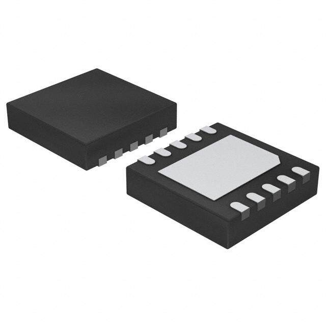
| 产品图片 |
|
| rohs | 符合RoHS无铅 / 符合限制有害物质指令(RoHS)规范要求 |
| 产品系列 | 电源管理 IC,低压差稳压器,NXP Semiconductors LD6806CX4/22H,315- |
| 数据手册 | |
| 产品型号 | LD6806CX4/22H,315 |
| PCN过时产品 | |
| 产品种类 | 低压差稳压器 |
| 供应商器件封装 | 4-WLCSP(0.76x0.76) |
| 其它名称 | 568-8426-1 |
| 包装 | 剪切带 (CT) |
| 商标 | NXP Semiconductors |
| 回动电压—最大值 | 60 mV |
| 安装类型 | 表面贴装 |
| 安装风格 | SMD/SMT |
| 封装 | Reel |
| 封装/外壳 | 4-XFBGA,WLCSP |
| 封装/箱体 | WLCSP-4 |
| 工作温度 | -40°C ~ 85°C |
| 工厂包装数量 | 9000 |
| 最大功率耗散 | 800 mW |
| 最大工作温度 | + 85 C |
| 最大输入电压 | 5.5 V |
| 最小工作温度 | - 40 C |
| 标准包装 | 1 |
| 特色产品 | http://www.digikey.cn/product-highlights/cn/zh/nxp-semiconductors-low-voltage-ldos/3032 |
| 电压-跌落(典型值) | 0.06V @ 200mA |
| 电压-输入 | 2.3 V ~ 5.5 V |
| 电压-输出 | 2.2V |
| 电流-输出 | 200mA |
| 电流-限制(最小值) | 300mA |
| 稳压器拓扑 | 正,固定式 |
| 稳压器数 | 1 |
| 输出电压 | 2.2 V |
| 输出电流 | 200 mA |
| 输出端数量 | 1 Output |
| 输出类型 | Fixed |


- 商务部:美国ITC正式对集成电路等产品启动337调查
- 曝三星4nm工艺存在良率问题 高通将骁龙8 Gen1或转产台积电
- 太阳诱电将投资9.5亿元在常州建新厂生产MLCC 预计2023年完工
- 英特尔发布欧洲新工厂建设计划 深化IDM 2.0 战略
- 台积电先进制程称霸业界 有大客户加持明年业绩稳了
- 达到5530亿美元!SIA预计今年全球半导体销售额将创下新高
- 英特尔拟将自动驾驶子公司Mobileye上市 估值或超500亿美元
- 三星加码芯片和SET,合并消费电子和移动部门,撤换高东真等 CEO
- 三星电子宣布重大人事变动 还合并消费电子和移动部门
- 海关总署:前11个月进口集成电路产品价值2.52万亿元 增长14.8%


PDF Datasheet 数据手册内容提取
LD6806 series Ultra low-dropout regulator, low noise, 200 mA Rev. 3 — 9 December 2011 Product data sheet 1. Product profile 1.1 General description The LD6806 series is a small-size Low-DropOut regulator (LDO) family with a typical voltage drop of 60mV at 200mA current rating. The device is available in three different surface-mounted packages, one 0.4mm pitch CSP, one leadless plastic package SOT886 and one gull wing package SOT753. The operating voltage ranges from 2.3 V to 5.5 V and the output voltage ranges from 1.2V to 3.6V. LD6806x/xxH devices show a high-ohmic state at the output pin, while the LD6806x/xxP contains a pull-down switching transistor, to provide a low-ohmic output stage when the device is disabled. All devices use the same regulator design and are manufactured in monolithic silicon technology. These features make the LD6806 series ideal for use in applications requiring component miniaturization, such as mobile phone handsets, cordless telephones and personal digital devices. 1.2 Features and benefits Input voltage range 2.3V to 5.5V Output voltage range 1.2V to 3.6V Dropout voltage 60mV at 200mA output rating Low quiescent current in shutdown mode (typical1.0A) 30V RMS output noise voltage (typical value) at 10Hzto100kHz Turn-on time just 200s 55dB Power Supply Rejection Ratio (PSRR) at1kHz Temperature watchdog Current limiter LD6806xxxH: high-ohmic (3-state) output state when disabled LD6806xxxP: low-ohmic output state when disabled Integrated ESD protection of 10kV Human Body Model WLCSP with 0.4mm pitch and package size of 0.76mm0.76mm0.47mm SOT886 leadless package 1.0mm1.45mm0.5mm SOT753 plastic surface-mounted device Pb-free, RoHS compliant and free of Halogen and Antimony (dark green compliant)
LD6806 series NXP Semiconductors Ultra low-dropout regulator, low noise, 200 mA 1.3 Applications Analog and digital interfaces requiring lower than standard supply voltage in mobile appliances such as mobile phones, media players and so on. 2. Pinning information 2.1 Pinning LD6806 OUT 1 6 IN bump A1 index area 1 2 A n.c. 2 5 n.c. 5 4 B GND 3 4 EN 001aao107 001aao333 transparent top view, 1 2 3 solder balls facing down Transparent top view Fig 1. Configuration for SOT753 Fig 2. Configuration for WLCSP4 Fig 3. Configuration for SOT886 2.2 Pin description Table 1. Pin description for SOT753 Symbol Pin Description IN 1 supply voltage input GND 2 supply ground EN 3 device enable input; active HIGH n.c. 4 not connected OUT 5 regulator output voltage Table 2. Pin description for WLCSP4 Symbol Pin Description GND A1 supply ground EN A2 device enable input; active HIGH OUT B1 regulator output voltage IN B2 supply voltage input Table 3. Pin description for SOT886 Symbol Pin Description OUT 1 regulator output voltage n.c. 2 not connected GND 3 supply ground LD6806_SER All information provided in this document is subject to legal disclaimers. © NXP B.V. 2011. All rights reserved. Product data sheet Rev. 3 — 9 December 2011 2 of 36
LD6806 series NXP Semiconductors Ultra low-dropout regulator, low noise, 200 mA Table 3. Pin description for SOT886 Symbol Pin Description EN 4 device enable input; active HIGH n.c. 5 not connected IN 6 supply voltage input 3. Ordering information Table 4. Ordering information Type number Package Name Description Version LD6806CX4/xxx WLCSP4 wafer level chip-size package; 4 bumps (22)[1] - LD6806CX4/C/xxx WLCSP4 wafer level chip-size package; 4 bumps (22) - with backside coating[1] LD6806F/xxx XSON6 plastic extremely thin small outline package; no SOT886 leads; 6terminals; body 11.450.5 mm LD6806TD/xxx TSOP5 plastic surface-mounted package; 5 leads SOT753 [1] Size 0.76mm0.76 mm. 3.1 Ordering options Further information on output voltage is available on request; see Section 21 “Contact information”. Table 5. Type number and nominal output voltage of high-ohmic output Type number Nominal Type number Nominal output output voltage voltage LD6806[CX4, CX4/C, F, TD]/12H 1.2V LD6806[CX4, CX4/C, F, TD]/23H 2.3V LD6806[CX4, CX4/C, F, TD]/13H 1.3V LD6806[CX4, CX4/C, F, TD]/25H 2.5V LD6806[CX4, CX4/C, F, TD]/14H 1.4V LD6806[CX4, CX4/C, F, TD]/28H 2.8V LD6806[CX4, CX4/C, F, TD]/16H 1.6V LD6806[CX4, CX4/C, F, TD]/29H 2.9V LD6806[CX4, CX4/C, F, TD]/18H 1.8V LD6806[CX4, CX4/C, F, TD]/30H 3.0V LD6806[CX4, CX4/C, F, TD]/20H 2.0V LD6806[CX4, CX4/C, F, TD]/33H 3.3V LD6806[CX4, CX4/C, F, TD]/22H 2.2V LD6806[CX4, CX4/C, F, TD]/36H 3.6V Table 6. Type number and nominal output voltage of low.ohmic output Type number Nominal Type number Nominal output output voltage voltage LD6806[CX4, CX4/C, F, TD]/12P 1.2V LD6806[CX4, CX4/C, F, TD]/23P 2.3V LD6806[CX4, CX4/C, F, TD]/13P 1.3V LD6806[CX4, CX4/C, F, TD]/25P 2.5V LD6806[CX4, CX4/C, F, TD]/14P 1.4V LD6806[CX4, CX4/C, F, TD]/28P 2.8V LD6806[CX4, CX4/C, F, TD]/16P 1.6V LD6806[CX4, CX4/C, F, TD]/29P 2.9V LD6806_SER All information provided in this document is subject to legal disclaimers. © NXP B.V. 2011. All rights reserved. Product data sheet Rev. 3 — 9 December 2011 3 of 36
LD6806 series NXP Semiconductors Ultra low-dropout regulator, low noise, 200 mA Table 6. Type number and nominal output voltage of low.ohmic output …continued Type number Nominal Type number Nominal output output voltage voltage LD6806[CX4, CX4/C, F, TD]/18P 1.8V LD6806[CX4, CX4/C, F, TD]/30P 3.0V LD6806[CX4, CX4/C, F, TD]/20P 2.0V LD6806[CX4, CX4/C, F, TD]/33P 3.3V LD6806[CX4, CX4/C, F, TD]/22P 2.2V LD6806[CX4, CX4/C, F, TD]/36P 3.6V 4. Block diagram VIN VOUT R1 VEN GEVNreEfeRreAnTceOR THERMAL PROTECTION R2 OVERCURRENT PROTECTION GND 001aan756 Fig 4. Block diagram of LD6806x/xxH VIN VOUT R1 VEN GEVNreEfeRreAnTcOeR THERMAL PROTECTION R2 OVER CURRENT PROTECTION GND 001aan299 Fig 5. Block diagram of LD6806x/xxP LD6806_SER All information provided in this document is subject to legal disclaimers. © NXP B.V. 2011. All rights reserved. Product data sheet Rev. 3 — 9 December 2011 4 of 36
LD6806 series NXP Semiconductors Ultra low-dropout regulator, low noise, 200 mA 5. Limiting values Table 7. Limiting valu es In accordance with the Absolute Maximum Rating System (IEC 60134). Voltages are referenced to GND (ground = 0V). Symbol Parameter Conditions Min Max Unit V voltage on pin IN 4ms transient 0.5 +6.0 V IN P total power dissipation LD6806CX4/xxx, [1] - 770 mW tot LD6806CX4/Cxxx LD6806F/xxx [1] - 450 mW LD6806TD/xxx [1] - 800 mW T storage temperature 55 +150 C stg T junction temperature 40 +125 C j T ambient temperature 40 +85 C amb V electrostatic discharge voltage human body model level 6 [2] 10 kV ESD machine model class 3 [3] - 400 V [1] The (absolute) maximum power dissipation depends on the junction temperature T. Higher power dissipation is allowed with lower j ambient temperatures. The conditions to determine the specified values are Tamb = 25 C and the use of a two layer PCB. [2] According to IEC61340-3-1. [3] According to JESD22-A115C. 6. Recommended operating conditions Table 8. Operating co nditions Voltages are referenced to GND (ground = 0 V). Symbol Parameter Conditions Min Max Unit T ambient temperature 40 +85 C amb T junction temperature - +125 C j Pin IN V voltage on pin IN 2.3 5.5 V IN Pin EN V voltage on pin EN 0 V V EN IN Pin OUT C external load capacitance [1] 1.0 - F L(ext) [1] See Section 10.1 “Output capacitor values”. LD6806_SER All information provided in this document is subject to legal disclaimers. © NXP B.V. 2011. All rights reserved. Product data sheet Rev. 3 — 9 December 2011 5 of 36
LD6806 series NXP Semiconductors Ultra low-dropout regulator, low noise, 200 mA 7. Thermal characteristics Table 9. Thermal cha racteristics Symbol Parameter Conditions Typ Unit R thermal resistance from junction to ambient LD6806CX4/xxx, [1][2] 130 K/W th(j-a) LD6806CX4/Cxxx LD6806F/xxx [1][2] 220 K/W LD6806TD/xxx [1][2] 125 K/W [1] The overall R can vary depending on the board layout. To minimize the effective R , all pins must have a solid connection to th(j-a) th(j-a) larger Cu layer areas for example to the power and ground layer. In multi-layer PCB applications, the second layer should be used to create a large heat spreader area directly below the LDO. If this layer is either ground or power, it should be connected with several vias to the top layer connecting to the device ground or supply. Avoid the use of solder-stop varnish under the chip. [2] Use the measurement data given for a rough estimation of the R in your application. The actual R value can vary in applications th(j-a) th(j-a) using different layer stacks and layouts. 8. Characteristics Table 10. Electrical ch aracteristics At recommended input voltages and T =40Cto+85C; voltages are referenced to GND (ground = 0 V); amb unlessotherwise specified. Symbol Parameter Conditions Min Typ Max Unit V output voltage variation V < 1.8 V; I = 1mA O OUT OUT T = +25C 3 0.5 +3 % amb 30C T +85C 4 - +4 % amb V 1.8 V; I = 1mA OUT OUT T = +25 C 2 0.5 +2 % amb 30C T +85C 3 - +3 % amb Line regulation error V /(V xV) relative output voltage V = (V + 0.2V) to 5.5V [1] 0.1 - +0.1 %/V O O I IN O(nom) variation with input voltage Load regulation error V /(V xI ) relative output voltage 1mA I 200mA O O O OUT variation with output current LD6806CX4/xxx, LD6806CX4/Cxxx - 0.0025 0.01 %/mA LD6806F/xxx, LD6806TD/xxx - 0.005 0.02 %/mA V dropout voltage I =200mA; V >V [1] do OUT IN O(nom) LD6806CX4/xxx, LD6806CX4/Cxxx - 60 100 mV LD6806F/xxx, LD6806TD/xxx - 80 130 mV V LOW-level input voltage pin EN 0 - 0.4 V IL V HIGH-level input voltage pin EN 1.4 - 5.5 V IH I current on pin OUT - - 200 mA OUT I peak output current V =(V +0.2V) to 5.5 V [1] OM IN O(nom) V > 1.8 V; 300 - - mA O(nom) V 0.95V OUT O(nom) V < 1.8 V; 300 - - mA O(nom) V 0.9V OUT O(nom) LD6806_SER All information provided in this document is subject to legal disclaimers. © NXP B.V. 2011. All rights reserved. Product data sheet Rev. 3 — 9 December 2011 6 of 36
LD6806 series NXP Semiconductors Ultra low-dropout regulator, low noise, 200 mA Table 10. Electrical characteristics …continued At recommended input voltages and T =40Cto+85C; voltages are referenced to GND (ground = 0 V); amb unlessotherwise specified. Symbol Parameter Conditions Min Typ Max Unit I short-circuit current pin OUT - 600 - mA sc I quiescent current V = 1.4V; I = 0mA - 70 100 A q EN OUT V = 1.4V; 1mA I 200mA - 155 250 A EN OUT V 0.4V - 0.1 1.0 A EN T shutdown temperature - 160 - C sd T shutdown temperature [2] - 20 - K sd(hys) hysteresis PSRR power supply rejection ratio V = V + 1V; I = 30mA; [1] - 55 - dB IN O(nom) OUT f = 1kHz ripple V RMS output noise voltage bandwidth=10Hzto100kHz; - 30 - V n(o)(RMS) C =1F L(ext) t regulator start-up time V =5.5V; V = 0.95V ; [1] - - 200 s startup(reg) IN OUT O(nom) I =200mA; C =1F OUT L(ext) t regulator shutdown time V =5.5V; C =1F [3] - 300 - s sd(reg) IN L(ext) R pull-down resistance [3] - 100 - pd [1] V =nominal output voltage (device specific). O(nom) [2] The junction temperature must decrease by T to enable the device after T was reached and the device was disabled. sd(hys) sd [3] LD6806x/xxP only. 9. Dynamic behavior All results described in Section9 are based on measurements of types LD6806CX4xxx and LD6806Fxxx from the LD6806 product series within Section 6 “Recommended operating conditions”. 9.1 Dropout The dropout voltage is defined as the smallest input to output voltage difference at a specified load current when the regulator operates within its linear region with the pass transistor functioning as a plain resistor. This means that the input voltage is below the nominal output voltage value. A small dropout voltage guaranties lower power consumption and efficiency maximization. LD6806_SER All information provided in this document is subject to legal disclaimers. © NXP B.V. 2011. All rights reserved. Product data sheet Rev. 3 — 9 December 2011 7 of 36
LD6806 series NXP Semiconductors Ultra low-dropout regulator, low noise, 200 mA 001aan929 001aan930 100 100 Vdo Vdo (mV) (mV) 80 80 (1) (2) (3) 60 60 (1) (2) 40 40 (3) 20 20 0 0 0 40 80 120 160 200 0 40 80 120 160 200 IOUT (mA) IOUT (mA) (1) +85C (1) +85C (2) +25C (2) +25C (3) 40C (3) 40C Fig 6. Dropout as a function of temperature for Fig 7. Dropout as a function of temperature for LD6806CX4/25H LD6806F/25H 001aan935 001aan936 100 100 Vdo Vdo (mV) (mV) 80 80 60 60 (1) (2) (3) 40 (1) 40 (2) (3) 20 20 0 0 0 40 80 120 160 200 0 40 80 120 160 200 IOUT (mA) IOUT (mA) (1) +85C (1) +85C (2) +25C (2) +25C (3) 40C (3) 40C Fig 8. Dropout as a function of temperature for Fig 9. Dropout as a function of temperature for LD6806CX4/36H LD6806F/36H LD6806_SER All information provided in this document is subject to legal disclaimers. © NXP B.V. 2011. All rights reserved. Product data sheet Rev. 3 — 9 December 2011 8 of 36
LD6806 series NXP Semiconductors Ultra low-dropout regulator, low noise, 200 mA 018aaa223 100 Vdo (mV) 80 60 (1) 40 (2) (3) 20 0 0 40 80 120 160 200 IOUT (mA) (1) +85C (2) +25C (3) 40C Fig 10. Dropout as a function of temperature for LD6806TD/36P 9.2 Output voltage variation The guaranteed output voltages are specified in Table10. 001aan942 001aan943 1.24 2.54 VOUT VOUT (V) (V) 1.22 2.52 (1) (1) (2) (2) (3) (3) 1.20 2.50 1.18 2.48 1.16 2.46 -60 -20 20 60 100 140 -60 -20 20 60 100 140 Tamb (°C) Tamb (°C) (1) I =1mA (1) I =1mA OUT OUT (2) IOUT=100mA (2) IOUT=100mA (3) IOUT=200mA (3) IOUT=200mA Fig 11. Output voltage variation for LD6806CX4/12H Fig 12. Output voltage variation for LD6806CX4/25H LD6806_SER All information provided in this document is subject to legal disclaimers. © NXP B.V. 2011. All rights reserved. Product data sheet Rev. 3 — 9 December 2011 9 of 36
LD6806 series NXP Semiconductors Ultra low-dropout regulator, low noise, 200 mA 9.3 Quiescent current Quiescent or ground current is the difference between the input and the output current of the regulator. 001aao106 001aan944 80 85 IGND (μA) IGND (μA) 75 80 (1) 70 (1) (2) 75 (2) 65 60 70 -60 -20 20 60 100 140 -60 -20 20 60 100 140 Tamb (°C) Tamb (°C) (1) I =10mA (1) I =10mA OUT OUT (2) I =0mA (2) I =0mA OUT OUT Fig 13. Quiescent current for LD6806CX4/12H Fig 14. Quiescent current for LD6806CX4/25H LD6806_SER All information provided in this document is subject to legal disclaimers. © NXP B.V. 2011. All rights reserved. Product data sheet Rev. 3 — 9 December 2011 10 of 36
LD6806 series NXP Semiconductors Ultra low-dropout regulator, low noise, 200 mA 9.4 Noise Output noise voltage of an LDO circuit is given as noise density or RMS output noise voltage over a defined range of frequencies (10Hzto100kHz). Permanent conditions are a constant output current and a ripple-free input voltage. The output noise voltage is generated by the LDO regulator. 001aan941 001aao104 10 10 noise noise (μV/√Hz) (μV/√Hz) 1 (1) 1 (1) (2) (2) (3) (3) (4) (4) (5) (5) (6) (6) 10-1 10-1 10-2 10-2 10 102 103 104 105 10 102 103 104 105 frequency (Hz) frequency (Hz) (1) 0mA (1) 0mA (2) 1mA (2) 1mA (3) 50mA (3) 50mA (4) 100mA (4) 100mA (5) 150mA (5) 150mA (6) 200mA (6) 200mA Fig 15. Noise density for LD6806CX4/25H Fig 16. Noise density for LD6806CX4/36H LD6806_SER All information provided in this document is subject to legal disclaimers. © NXP B.V. 2011. All rights reserved. Product data sheet Rev. 3 — 9 December 2011 11 of 36
LD6806 series NXP Semiconductors Ultra low-dropout regulator, low noise, 200 mA 9.5 Line regulation Line regulation response is the capability of the circuit to maintain the nominal output voltage while varying the input voltage. Regulation%V = ----V----O----U---T-----1---0---0---- V V IN OUT 001aan925 001aan926 6 2.0 6 2.0 (1) VOUT (1) VOUT VIN (V) VIN (V) (V) 1.8 (V) 1.8 4 4 1.6 1.6 1.4 1.4 2 2 (2) (2) 1.2 1.2 0 1.0 0 1.0 0 0.2 0.4 0.6 0.8 0 0.1 0.2 0.3 0.4 0.5 0.6 0.7 time (ms) time (ms) (1) V (1) V IN IN (2) V (2) V OUT OUT Fig 17. Line regulation for LD6806CX4/12H Fig 18. Line regulation for LD6806F/12H 001aan931 001aan932 6 2.55 6 2.55 (1) VOUT (1) VOUT 2.54 (V) 2.54 (V) VIN VIN (V) 2.53 (V) 2.53 2.52 2.52 4 4 2.51 2.51 (2) (2) 2.50 2.50 2.49 2.49 2 2 2.48 2.48 2.47 2.47 2.46 2.46 0 2.45 0 2.45 0 0.1 0.2 0.3 0.4 0 0.1 0.2 0.3 0.4 time (ms) time (ms) (1) V (1) V IN IN (2) V (2) V OUT OUT Fig 19. Line regulation for LD6806CX4/25H Fig 20. Line regulation for LD6806F/25H LD6806_SER All information provided in this document is subject to legal disclaimers. © NXP B.V. 2011. All rights reserved. Product data sheet Rev. 3 — 9 December 2011 12 of 36
LD6806 series NXP Semiconductors Ultra low-dropout regulator, low noise, 200 mA 001aan937 001aan938 6 3.75 6 3.75 (1) (1) VIN VOUT VIN VOUT (V) (V) (V) (V) 4 3.65 4 3.65 (2) (2) 2 3.55 2 3.55 0 3.45 0 3.45 0 0.2 0.4 0.6 0.8 0 0.1 0.2 0.3 0.4 0.5 0.6 0.7 time (ms) time (ms) (1) V (1) V IN IN (2) V (2) V OUT OUT Fig 21. Line regulation for LD6806CX4/36H Fig 22. Line regulation for LD6806F/36H 9.6 Load regulation Load regulation is the capability of the circuit to maintain the nominal output voltage while varying the output load current. V ---------O----U---T---100 V Load regulation%mA = -----O-----n---o--m-------------------- I OUTmax 001aan927 001aan928 0.5 1.3 0.5 1.30 VOUT VOUT (2) (V) (V) IOUT 1.2 IOUT 1.25 (A) (A) 1.1 1.20 (2) 0.3 0.3 1.0 1.15 (1) (1) 0.9 1.10 0.8 1.05 0.1 0.1 0.7 1.00 0.6 0.95 -0.1 0.5 -0.1 0.90 0 0.1 0.2 0.3 0.4 0.5 0.6 0.7 0 0.2 0.4 0.6 0.8 time (ms) time (ms) (1) I (1) I OUT OUT (2) V (2) V OUT OUT Fig 23. Load regulation for LD6806CX4/12H Fig 24. Load regulation for LD6806F/12H LD6806_SER All information provided in this document is subject to legal disclaimers. © NXP B.V. 2011. All rights reserved. Product data sheet Rev. 3 — 9 December 2011 13 of 36
LD6806 series NXP Semiconductors Ultra low-dropout regulator, low noise, 200 mA 001aan933 001aan934 0.5 2.6 0.5 2.6 IOUT VOUT IOUT VOUT (A) (V) (A) (V) (2) (2) 0.3 2.5 0.3 2.5 (1) 0.1 2.4 0.1 2.4 (1) -0.1 2.3 -0.1 2.3 0 0.1 0.2 0.3 0.4 0 0.1 0.2 0.3 0.4 time (ms) time (ms) (1) I (1) I OUT OUT (2) V (2) V OUT OUT Fig 25. Load regulation for LD6806CX4/25H Fig 26. Load regulation for LD6806F/25H 001aan939 001aan940 0.5 3.7 0.5 3.7 IOUT VOUT IOUT VOUT (A) (V) (A) (V) (2) 0.3 (2) 3.6 0.3 3.6 (1) 0.1 3.5 0.1 3.5 (1) -0.1 3.4 -0.1 3.4 0 0.1 0.2 0.3 0.4 0.5 0.6 0.7 0 0.1 0.2 0.3 0.4 0.5 0.6 0.7 time (ms) time (ms) (1) I (1) I OUT OUT (2) V (2) V OUT OUT Fig 27. Load regulation for LD6806CX4/36H Fig 28. Load regulation for LD6806F/36H LD6806_SER All information provided in this document is subject to legal disclaimers. © NXP B.V. 2011. All rights reserved. Product data sheet Rev. 3 — 9 December 2011 14 of 36
LD6806 series NXP Semiconductors Ultra low-dropout regulator, low noise, 200 mA 9.7 Start-up and shut down Start-up time defines the time needed for the LDO to achieve 95% of its typical output voltage level after activation via the enable pin. Shut down time defines the time needed for the LDO to pull-down the output voltage to 10% of its nominal output voltage after deactivation via the enable pin. 001aan946 001aan947 1.6 3 1.4 3 VOUT Venable VOUT Venable (1) (V) (V) (V) (V) 2.5 1.2 2.5 1.2 1 (2) 2 2 0.8 0.8 1.5 (1) (2) 1.5 0.6 1 1 0.4 0.4 0.5 0.5 0.2 0 0 0 0 0 0.05 0.1 0.15 0.2 0 0.1 0.2 0.3 0.4 time (ms) time (ms) (1) V . (1) V . EN EN (2) VOUT. (2) VOUT. Fig 29. Start-up for LD6806CX4/23H Fig 30. Shut down for LD6806F/25P LD6806_SER All information provided in this document is subject to legal disclaimers. © NXP B.V. 2011. All rights reserved. Product data sheet Rev. 3 — 9 December 2011 15 of 36
LD6806 series NXP Semiconductors Ultra low-dropout regulator, low noise, 200 mA 9.8 Power Supply Rejection Ratio (PSRR) PSRR stands for the capability of the regulator to suppress unwanted signals on the input voltage like noise or ripples. V PSRRdB = 20log----o---u---t---r--i--p--p---l--e-- for all frequencies V inripple 001aan945 001aao105 0 0 PSRR (dB) -10 PSSR (dB) -20 -20 -30 -40 (1) (2) (3) (1) -40 (4) (2) -50 (3) (4) -60 -70 -60 102 103 104 105 102 103 104 105 frequency (Hz) frequency (Hz) (1) 1mA (1) 1mA (2) 50mA (2) 50mA (3) 100mA (3) 100mA (4) 200mA (4) 200mA Fig 31. PSRR for LD6806CX4/25H Fig 32. PSRR for LD6806CX4/36H LD6806_SER All information provided in this document is subject to legal disclaimers. © NXP B.V. 2011. All rights reserved. Product data sheet Rev. 3 — 9 December 2011 16 of 36
LD6806 series NXP Semiconductors Ultra low-dropout regulator, low noise, 200 mA 9.9 Enable threshold voltage An active HIGH signal enables the LDO when the signal exceeds the minimum input HIGH voltage threshold. The device is in Off state as long the signal is below the maximum LOW threshold. The input voltage threshold is independent from the LDO supply voltage. 001aan808 3.5 VOUT (V) 2.5 1.5 (2) (1) 0.5 -0.5 0.3 0.5 0.7 0.9 1.1 1.3 1.5 VEN (V) (1) LOW to HIGH (2) HIGH to LOW Fig 33. Enable threshold voltage LD6806_SER All information provided in this document is subject to legal disclaimers. © NXP B.V. 2011. All rights reserved. Product data sheet Rev. 3 — 9 December 2011 17 of 36
LD6806 series NXP Semiconductors Ultra low-dropout regulator, low noise, 200 mA 10. Application information 10.1 Output capacitor values The LD6806 series requires external capacitors at the output to guarantee a stable regulator behavior. Also an input capacitor is recommended to keep the input voltage stable. These capacitors should not under-run the specified minimum Equivalent Series Resistance (ESR). The absolute value of the total capacitance attached to the output pin OUT influences the shutdown time (t ) of the LD6806 series. sd(reg) Table 11. External load capacitor Symbol Parameter Conditions Min Typ Max Unit C external load capacitance [1] - 1.0 - F L(ext) ESR equivalent series resistance 5 - 500 m [1] The minimum value of capacitance for stability and correct operation is 0.7F. The capacitor tolerance should be 30% or better over the temperature range. The full range of operating conditions for the capacitor in the application should be considered during device selection to ensure that this minimum capacitance specification is met. The recommended capacitor type is X7R to meet the full device temperature specification of 40Cto+125C. IN OUT IN OUT 1μF 1μF EN GND 001aan647 Fig 34. Application diagram 11. Test information 11.1 Quality information This product has been qualified in accordance with NX2-00001 NXP Semiconductors Quality and Reliability Specification and is suitable for use in consumer applications. LD6806_SER All information provided in this document is subject to legal disclaimers. © NXP B.V. 2011. All rights reserved. Product data sheet Rev. 3 — 9 December 2011 18 of 36
LD6806 series NXP Semiconductors Ultra low-dropout regulator, low noise, 200 mA 12. Package outline WLCSP4: wafer level chip-size package; 4 bumps (2 x 2) D bump A1 index area A2 E A A1 detail X e b B e A 1 2 X European projection wlcsp4_2x2_po Fig 35. Package outline WLCSP4 Table 12. Dimensions of LD6806CX4/xxx for package outline WLCSP4; see Figure35 Symbol Min Typ Max Unit A 0.44 0.47 0.50 mm A 0.18 0.20 0.22 mm 1 A 0.26 0.27 0.28 mm 2 b 0.21 0.26 0.31 mm D 0.71 0.76 0.81 mm E 0.71 0.76 0.81 mm e - 0.4 - mm LD6806_SER All information provided in this document is subject to legal disclaimers. © NXP B.V. 2011. All rights reserved. Product data sheet Rev. 3 — 9 December 2011 19 of 36
LD6806 series NXP Semiconductors Ultra low-dropout regulator, low noise, 200 mA WLCSP4: wafer level chip-size package with backside coating; 4 bumps (2 x 2) D A3 bump A1 index area A2 A E A1 detail X e b B e A 1 2 European X projection wlcsp4_2x2_c_po Fig 36. Package outline WLCSP4 with backside coating Table 13. Dimensions of LD6806CX4/Cxxx for package outline WLCSP4 with backside coating; see Figure36 Symbol Min Typ Max Unit A 0.47 0.51 0.55 mm A 0.18 0.20 0.22 mm 1 A 0.26 0.27 0.28 mm 2 A 0.03 0.04 0.05 mm 3 b 0.21 0.26 0.31 mm D 0.71 0.76 0.81 mm E 0.71 0.76 0.81 mm e - 0.4 - mm LD6806_SER All information provided in this document is subject to legal disclaimers. © NXP B.V. 2011. All rights reserved. Product data sheet Rev. 3 — 9 December 2011 20 of 36
LD6806 series NXP Semiconductors Ultra low-dropout regulator, low noise, 200 mA XSON6: plastic extremely thin small outline package; no leads; 6 terminals; body 1 x 1.45 x 0.5 mm SOT886 b 1 2 3 4× L1 L (2) e 6 5 4 e1 e1 6× A (2) A1 D E terminal 1 index area 0 1 2 mm scale DIMENSIONS (mm are the original dimensions) UNIT mA(a1x) mAa1x b D E e e1 L L1 0.25 1.5 1.05 0.35 0.40 mm 0.5 0.04 0.6 0.5 0.17 1.4 0.95 0.27 0.32 Notes 1. Including plating thickness. 2. Can be visible in some manufacturing processes. OUTLINE REFERENCES EUROPEAN ISSUE DATE VERSION IEC JEDEC JEITA PROJECTION 04-07-15 SOT886 MO-252 04-07-22 Fig 37. Package outline SOT886 (XSON6) LD6806_SER All information provided in this document is subject to legal disclaimers. © NXP B.V. 2011. All rights reserved. Product data sheet Rev. 3 — 9 December 2011 21 of 36
LD6806 series NXP Semiconductors Ultra low-dropout regulator, low noise, 200 mA Plastic surface-mounted package; 5 leads SOT753 D B E A X y HE v M A 5 4 Q A A1 c 1 2 3 Lp detail X e bp w M B 0 1 2 mm scale DIMENSIONS (mm are the original dimensions) UNIT A A1 bp c D E e HE Lp Q v w y 1.1 0.100 0.40 0.26 3.1 1.7 3.0 0.6 0.33 mm 0.95 0.2 0.2 0.1 0.9 0.013 0.25 0.10 2.7 1.3 2.5 0.2 0.23 OUTLINE REFERENCES EUROPEAN ISSUE DATE VERSION IEC JEDEC JEITA PROJECTION 02-04-16 SOT753 SC-74A 06-03-16 Fig 38. SOT753; Plastic surface-mounted package; 5 leads LD6806_SER All information provided in this document is subject to legal disclaimers. © NXP B.V. 2011. All rights reserved. Product data sheet Rev. 3 — 9 December 2011 22 of 36
LD6806 series NXP Semiconductors Ultra low-dropout regulator, low noise, 200 mA 13. Soldering D e c (4×) e E solder resist solder paste = solderland f occupied area (4×) Dimensions in mm wlcsp4_2x2_fr Fig 39. Soldering footprint WLCSP4 Table 14. Dimensions of soldering footprint WLCSP4; see Figure39 Symbol Min Typ Max Unit c - 0.25 - mm D 0.71 0.76 0.81 mm E 0.71 0.76 0.81 mm e - 0.4 - mm f - 0.325 - mm 1.250 0.675 0.370 (6×) 0.500 1.700 solder resist 0.500 solder paste = solderland 0.270 (6×) occupied area Dimensions in mm 0.325 0.425 (6×) (6×) sot886_fr Fig 40. Soldering footprint SOT886 (XSON6) LD6806_SER All information provided in this document is subject to legal disclaimers. © NXP B.V. 2011. All rights reserved. Product data sheet Rev. 3 — 9 December 2011 23 of 36
LD6806 series NXP Semiconductors Ultra low-dropout regulator, low noise, 200 mA 3.45 1.95 0.45 0.55 solder lands 0.95 (5×) (5×) 3.3 2.825 solder resist 0.95 solder paste occupied area 2.4 Dimensions in mm 0.7 (5×) 0.8 (5×) sot753_fr Fig 41. SOT753 (TSOP5); Reflow soldering footprint 5.3 1.5 (4×) solder lands 1.475 solder resist 5.05 0.45 occupied area 1.475 Dimensions in mm preferred transport direction during soldering 1.45 (5×) 2.85 sot753_fw Fig 42. SOT753 (TSOP5); Wave soldering footprint 14. Soldering of WLCSP packages 14.1 Introduction to soldering WLCSP packages This text provides a very brief insight into a complex technology. A more in-depth account of soldering WLCSP (Wafer Level Chip-Size Packages) can be found in application note AN10439 “Wafer Level Chip Scale Package” and in application note AN10365 “Surface mount reflow soldering description”. Wave soldering is not suitable for this package. LD6806_SER All information provided in this document is subject to legal disclaimers. © NXP B.V. 2011. All rights reserved. Product data sheet Rev. 3 — 9 December 2011 24 of 36
LD6806 series NXP Semiconductors Ultra low-dropout regulator, low noise, 200 mA All NXP WLCSP packages are lead-free. 14.2 Board mounting Board mounting of a WLCSP requires several steps: 1. Solder paste printing on the PCB 2. Component placement with a pick and place machine 3. The reflow soldering itself 14.3 Reflow soldering Key characteristics in reflow soldering are: • Lead-free versus SnPb soldering; note that a lead-free reflow process usually leads to higher minimum peak temperatures (see Figure43) than a PbSn process, thus reducing the process window • Solder paste printing issues, such as smearing, release, and adjusting the process window for a mix of large and small components on one board • Reflow temperature profile; this profile includes preheat, reflow (in which the board is heated to the peak temperature), and cooling down. It is imperative that the peak temperature is high enough for the solder to make reliable solder joints (a solder paste characteristic) while being low enough that the packages and/or boards are not damaged. The peak temperature of the package depends on package thickness and volume and is classified in accordance with Table15. Table 15. Lead-free process (from J-STD-020C) Package thickness (mm) Package reflow temperature (C) Volume (mm3) < 350 350 to 2000 > 2000 < 1.6 260 260 260 1.6 to 2.5 260 250 245 > 2.5 250 245 245 Moisture sensitivity precautions, as indicated on the packing, must be respected at all times. Studies have shown that small packages reach higher temperatures during reflow soldering, see Figure43. LD6806_SER All information provided in this document is subject to legal disclaimers. © NXP B.V. 2011. All rights reserved. Product data sheet Rev. 3 — 9 December 2011 25 of 36
LD6806 series NXP Semiconductors Ultra low-dropout regulator, low noise, 200 mA maximum peak temperature = MSL limit, damage level temperature minimum peak temperature = minimum soldering temperature peak temperature time 001aac844 MSL: Moisture Sensitivity Level Fig 43. Temperature profiles for large and small components For further information on temperature profiles, refer to application note AN10365 “Surface mount reflow soldering description”. 14.3.1 Stand off The stand off between the substrate and the chip is determined by: • The amount of printed solder on the substrate • The size of the solder land on the substrate • The bump height on the chip The higher the stand off, the better the stresses are released due to TEC (Thermal Expansion Coefficient) differences between substrate and chip. 14.3.2 Quality of solder joint A flip-chip joint is considered to be a good joint when the entire solder land has been wetted by the solder from the bump. The surface of the joint should be smooth and the shape symmetrical. The soldered joints on a chip should be uniform. Voids in the bumps after reflow can occur during the reflow process in bumps with high ratio of bump diameter to bump height, i.e. low bumps with large diameter. No failures have been found to be related to these voids. Solder joint inspection after reflow can be done with X-ray to monitor defects such as bridging, open circuits and voids. 14.3.3 Rework In general, rework is not recommended. By rework we mean the process of removing the chip from the substrate and replacing it with a new chip. If a chip is removed from the substrate, most solder balls of the chip will be damaged. In that case it is recommended not to re-use the chip again. LD6806_SER All information provided in this document is subject to legal disclaimers. © NXP B.V. 2011. All rights reserved. Product data sheet Rev. 3 — 9 December 2011 26 of 36
LD6806 series NXP Semiconductors Ultra low-dropout regulator, low noise, 200 mA Device removal can be done when the substrate is heated until it is certain that all solder joints are molten. The chip can then be carefully removed from the substrate without damaging the tracks and solder lands on the substrate. Removing the device must be done using plastic tweezers, because metal tweezers can damage the silicon. The surface of the substrate should be carefully cleaned and all solder and flux residues and/or underfill removed. When a new chip is placed on the substrate, use the flux process instead of solder on the solder lands. Apply flux on the bumps at the chip side as well as on the solder pads on the substrate. Place and align the new chip while viewing with a microscope. To reflow the solder, use the solder profile shown in application note AN10365 “Surface mount reflow soldering description”. 14.3.4 Cleaning Cleaning can be done after reflow soldering. 15. Soldering of SMD packages This text provides a very brief insight into a complex technology. A more in-depth account of soldering ICs can be found in Application Note AN10365 “Surface mount reflow soldering description”. 15.1 Introduction to soldering Soldering is one of the most common methods through which packages are attached to Printed Circuit Boards (PCBs), to form electrical circuits. The soldered joint provides both the mechanical and the electrical connection. There is no single soldering method that is ideal for all IC packages. Wave soldering is often preferred when through-hole and Surface Mount Devices (SMDs) are mixed on one printed wiring board; however, it is not suitable for fine pitch SMDs. Reflow soldering is ideal for the small pitches and high densities that come with increased miniaturization. 15.2 Wave and reflow soldering Wave soldering is a joining technology in which the joints are made by solder coming from a standing wave of liquid solder. The wave soldering process is suitable for the following: • Through-hole components • Leaded or leadless SMDs, which are glued to the surface of the printed circuit board Not all SMDs can be wave soldered. Packages with solder balls, and some leadless packages which have solder lands underneath the body, cannot be wave soldered. Also, leaded SMDs with leads having a pitch smaller than ~0.6mm cannot be wave soldered, due to an increased probability of bridging. The reflow soldering process involves applying solder paste to a board, followed by component placement and exposure to a temperature profile. Leaded packages, packages with solder balls, and leadless packages are all reflow solderable. Key characteristics in both wave and reflow soldering are: • Board specifications, including the board finish, solder masks and vias • Package footprints, including solder thieves and orientation LD6806_SER All information provided in this document is subject to legal disclaimers. © NXP B.V. 2011. All rights reserved. Product data sheet Rev. 3 — 9 December 2011 27 of 36
LD6806 series NXP Semiconductors Ultra low-dropout regulator, low noise, 200 mA • The moisture sensitivity level of the packages • Package placement • Inspection and repair • Lead-free soldering versus SnPb soldering 15.3 Wave soldering Key characteristics in wave soldering are: • Process issues, such as application of adhesive and flux, clinching of leads, board transport, the solder wave parameters, and the time during which components are exposed to the wave • Solder bath specifications, including temperature and impurities 15.4 Reflow soldering Key characteristics in reflow soldering are: • Lead-free versus SnPb soldering; note that a lead-free reflow process usually leads to higher minimum peak temperatures (see Figure44) than a SnPb process, thus reducing the process window • Solder paste printing issues including smearing, release, and adjusting the process window for a mix of large and small components on one board • Reflow temperature profile; this profile includes preheat, reflow (in which the board is heated to the peak temperature) and cooling down. It is imperative that the peak temperature is high enough for the solder to make reliable solder joints (a solder paste characteristic). In addition, the peak temperature must be low enough that the packages and/or boards are not damaged. The peak temperature of the package depends on package thickness and volume and is classified in accordance with Table16 and17 Table 16. SnPb eutectic process (from J-STD-020C) Package thickness (mm) Package reflow temperature (C) Volume (mm3) < 350 350 < 2.5 235 220 2.5 220 220 T able 17. Lead-free process (from J-STD-020C) Package thickness (mm) Package reflow temperature (C) Volume (mm3) < 350 350 to 2000 > 2000 < 1.6 260 260 260 1.6 to 2.5 260 250 245 > 2.5 250 245 245 Moisture sensitivity precautions, as indicated on the packing, must be respected at all times. LD6806_SER All information provided in this document is subject to legal disclaimers. © NXP B.V. 2011. All rights reserved. Product data sheet Rev. 3 — 9 December 2011 28 of 36
LD6806 series NXP Semiconductors Ultra low-dropout regulator, low noise, 200 mA Studies have shown that small packages reach higher temperatures during reflow soldering, see Figure44. maximum peak temperature = MSL limit, damage level temperature minimum peak temperature = minimum soldering temperature peak temperature time 001aac844 MSL: Moisture Sensitivity Level Fig 44. Temperature profiles for large and small components For further information on temperature profiles, refer to Application Note AN10365 “Surface mount reflow soldering description”. 16. Mounting 16.1 PCB design guidelines It is recommended, for optimum performance, to use a Non-Solder Mask Defined (NSMD), also known as a copper-defined design, incorporating laser-drilled micro-vias connecting the ground pads to a buried ground-plane layer. This results in the lowest possible ground inductance and provides the best high frequency and ESD performance. Refer to Table18 for the recommended PCB design parameters. Table 18. Recommended PCB design parameters Parameter Value or specification PCB pad diameter 250m Micro-via diameter 100m (0.004inch) Solder mask aperture diameter 325m Copper thickness 20m to 40m Copper finish AuNi or OSP PCB material FR4 LD6806_SER All information provided in this document is subject to legal disclaimers. © NXP B.V. 2011. All rights reserved. Product data sheet Rev. 3 — 9 December 2011 29 of 36
LD6806 series NXP Semiconductors Ultra low-dropout regulator, low noise, 200 mA 16.2 PCB assembly guidelines for Pb-free soldering Table 19. Assembly recommendations Parameter Value or specification Solder screen aperture diameter 250m Solder screen thickness 100m (0.004inch) Solder paste: Pb-free SnAg (3% to 4%); Cu (0.5% to 0.9%) Solder to flux ratio 50:50 Solder reflow profile seeFigure45 T (°C) Treflow(peak) 250 230 cooling rate 217 preheat t (s) t1 t2 t3 t4 t5 001aai943 The device is capable of withstanding at least three reflows at this profile. Fig 45. Pb-free solder reflow profile T able 20. Characteristics Symbol Parameter Conditions Min Typ Max Unit T peak reflow temperature 230 - 260 C reflow(peak) t time1 soak time 60 - 180 s 1 t time2 time during T250C - - 30 s 2 t time3 time during T230C 10 - 50 s 3 t time4 time during T>217C 30 - 150 s 4 t time5 - - 540 s 5 dT/dt rate of change of cooling rate - - 6 C/s temperature preheat 2.5 - 4.0 C/s LD6806_SER All information provided in this document is subject to legal disclaimers. © NXP B.V. 2011. All rights reserved. Product data sheet Rev. 3 — 9 December 2011 30 of 36
LD6806 series NXP Semiconductors Ultra low-dropout regulator, low noise, 200 mA 17. Abbreviations Table 21. Abbreviations Acronym Description CSP Chip-Size Package DUT Device Under Test EMI ElectroMagnetic Interference ESD ElectroStatic Discharge FR4 Flame Retard 4 HBM Human Body Model LDO Low DropOut MM Machine Model NSMD Non-Solder Mask Design OSP Organic Solderability Preservation PCB Printed-Circuit Board PSRR Power Supply Rejection Ratio PSU Power Supply Unit QRS Quality and Reliability Specification RMS Root Mean Square WLCSP Wafer Level Chip-Size Package 18. References [1] IEC 60134 — Rating systems for electronic tubes and valves and analogous semiconductor devices [2] IEC 61340-3-1 — Methods for simulation of electrostatic effects - Human body model (HBM) electrostatic discharge test waveforms [3] JESD22-A115C — Electrostatic discharge (ESD) Sensitivity Testing Machine Model(MM) [4] NX2-00001 — NXP Semiconductors Quality and Reliability Specification [5] AN10439 — Wafer Level Chip Size Package [6] AN10365 — Surface mount reflow soldering description LD6806_SER All information provided in this document is subject to legal disclaimers. © NXP B.V. 2011. All rights reserved. Product data sheet Rev. 3 — 9 December 2011 31 of 36
LD6806 series NXP Semiconductors Ultra low-dropout regulator, low noise, 200 mA 19. Revision history Table 22. Revision history Document ID Release date Data sheet status Change notice Supersedes LD6806_SER v.3 20111209 Product data sheet - LD6806_SER v.2 Modifications: • WLCSP4 package with backside coating added • SOT753 package added • Subtype LD6806x/xxP introduced • Minor text changes LD6806_SER v.2 20110719 Product data sheet - LD6806_SER v.1 Modifications: • Descriptive title updated • Table5: title changed • Table10: three parameters updated • Table3: pin number updated • Section9.4 and Section9.8 drawings updated • Section16: values updated • Minor text changes LD6806_SER v.1 20110516 Preliminary data sheet - - LD6806_SER All information provided in this document is subject to legal disclaimers. © NXP B.V. 2011. All rights reserved. Product data sheet Rev. 3 — 9 December 2011 32 of 36
LD6806 series NXP Semiconductors Ultra low-dropout regulator, low noise, 200 mA 20. Legal information 20.1 Data sheet status Document status[1][2] Product status[3] Definition Objective [short] data sheet Development This document contains data from the objective specification for product development. Preliminary [short] data sheet Qualification This document contains data from the preliminary specification. Product [short] data sheet Production This document contains the product specification. [1] Please consult the most recently issued document before initiating or completing a design. [2] The term ‘short data sheet’ is explained in section “Definitions”. [3] The product status of device(s) described in this document may have changed since this document was published and may differ in case of multiple devices. The latest product status information is available on the Internet at URLhttp://www.nxp.com. 20.2 Definitions malfunction of an NXP Semiconductors product can reasonably be expected to result in personal injury, death or severe property or environmental damage. NXP Semiconductors accepts no liability for inclusion and/or use of Draft — The document is a draft version only. The content is still under NXP Semiconductors products in such equipment or applications and internal review and subject to formal approval, which may result in therefore such inclusion and/or use is at the customer’s own risk. modifications or additions. NXP Semiconductors does not give any representations or warranties as to the accuracy or completeness of Applications — Applications that are described herein for any of these information included herein and shall have no liability for the consequences of products are for illustrative purposes only. NXP Semiconductors makes no use of such information. representation or warranty that such applications will be suitable for the specified use without further testing or modification. Short data sheet — A short data sheet is an extract from a full data sheet with the same product type number(s) and title. A short data sheet is intended Customers are responsible for the design and operation of their applications for quick reference only and should not be relied upon to contain detailed and and products using NXP Semiconductors products, and NXP Semiconductors full information. For detailed and full information see the relevant full data accepts no liability for any assistance with applications or customer product sheet, which is available on request via the local NXP Semiconductors sales design. It is customer’s sole responsibility to determine whether the NXP office. In case of any inconsistency or conflict with the short data sheet, the Semiconductors product is suitable and fit for the customer’s applications and full data sheet shall prevail. products planned, as well as for the planned application and use of customer’s third party customer(s). Customers should provide appropriate Product specification — The information and data provided in a Product design and operating safeguards to minimize the risks associated with their data sheet shall define the specification of the product as agreed between applications and products. NXP Semiconductors and its customer, unless NXP Semiconductors and NXP Semiconductors does not accept any liability related to any default, customer have explicitly agreed otherwise in writing. In no event however, damage, costs or problem which is based on any weakness or default in the shall an agreement be valid in which the NXP Semiconductors product is customer’s applications or products, or the application or use by customer’s deemed to offer functions and qualities beyond those described in the third party customer(s). Customer is responsible for doing all necessary Product data sheet. testing for the customer’s applications and products using NXP Semiconductors products in order to avoid a default of the applications and 20.3 Disclaimers the products or of the application or use by customer’s third party customer(s). NXP does not accept any liability in this respect. Limited warranty and liability — Information in this document is believed to Limiting values — Stress above one or more limiting values (as defined in be accurate and reliable. However, NXP Semiconductors does not give any the Absolute Maximum Ratings System of IEC60134) will cause permanent representations or warranties, expressed or implied, as to the accuracy or damage to the device. Limiting values are stress ratings only and (proper) completeness of such information and shall have no liability for the operation of the device at these or any other conditions above those given in consequences of use of such information. the Recommended operating conditions section (if present) or the Characteristics sections of this document is not warranted. Constant or In no event shall NXP Semiconductors be liable for any indirect, incidental, repeated exposure to limiting values will permanently and irreversibly affect punitive, special or consequential damages (including - without limitation - lost the quality and reliability of the device. profits, lost savings, business interruption, costs related to the removal or replacement of any products or rework charges) whether or not such Terms and conditions of commercial sale — NXP Semiconductors damages are based on tort (including negligence), warranty, breach of products are sold subject to the general terms and conditions of commercial contract or any other legal theory. sale, as published at http://www.nxp.com/profile/terms, unless otherwise Notwithstanding any damages that customer might incur for any reason agreed in a valid written individual agreement. In case an individual whatsoever, NXP Semiconductors’ aggregate and cumulative liability towards agreement is concluded only the terms and conditions of the respective customer for the products described herein shall be limited in accordance agreement shall apply. NXP Semiconductors hereby expressly objects to with the Terms and conditions of commercial sale of NXP Semiconductors. applying the customer’s general terms and conditions with regard to the purchase of NXP Semiconductors products by customer. Right to make changes — NXP Semiconductors reserves the right to make changes to information published in this document, including without No offer to sell or license — Nothing in this document may be interpreted or limitation specifications and product descriptions, at any time and without construed as an offer to sell products that is open for acceptance or the grant, notice. This document supersedes and replaces all information supplied prior conveyance or implication of any license under any copyrights, patents or to the publication hereof. other industrial or intellectual property rights. Suitability for use — NXP Semiconductors products are not designed, Export control — This document as well as the item(s) described herein authorized or warranted to be suitable for use in life support, life-critical or may be subject to export control regulations. Export might require a prior safety-critical systems or equipment, nor in applications where failure or authorization from competent authorities. LD6806_SER All information provided in this document is subject to legal disclaimers. © NXP B.V. 2011. All rights reserved. Product data sheet Rev. 3 — 9 December 2011 33 of 36
LD6806 series NXP Semiconductors Ultra low-dropout regulator, low noise, 200 mA Non-automotive qualified products — Unless this data sheet expressly NXP Semiconductors’ specifications such use shall be solely at customer’s states that this specific NXP Semiconductors product is automotive qualified, own risk, and (c) customer fully indemnifies NXP Semiconductors for any the product is not suitable for automotive use. It is neither qualified nor tested liability, damages or failed product claims resulting from customer design and in accordance with automotive testing or application requirements. NXP use of the product for automotive applications beyond NXP Semiconductors’ Semiconductors accepts no liability for inclusion and/or use of standard warranty and NXP Semiconductors’ product specifications. non-automotive qualified products in automotive equipment or applications. In the event that customer uses the product for design-in and use in 20.4 Trademarks automotive applications to automotive specifications and standards, customer (a) shall use the product without NXP Semiconductors’ warranty of the Notice: All referenced brands, product names, service names and trademarks product for such automotive applications, use and specifications, and (b) are the property of their respective owners. whenever customer uses the product for automotive applications beyond 21. Contact information For more information, please visit: http://www.nxp.com For sales office addresses, please send an email to: salesaddresses@nxp.com LD6806_SER All information provided in this document is subject to legal disclaimers. © NXP B.V. 2011. All rights reserved. Product data sheet Rev. 3 — 9 December 2011 34 of 36
LD6806 series NXP Semiconductors Ultra low-dropout regulator, low noise, 200 mA 22. Tables Table 1. Pin description for SOT753 . . . . . . . . . . . . . . . .2 outline WLCSP4; see Figure35 . . . . . . . . . . .19 Table 2. Pin description for WLCSP4. . . . . . . . . . . . . . . .2 Table 13. Dimensions of LD6806CX4/Cxxx for package Table 3. Pin description for SOT886 . . . . . . . . . . . . . . . .2 outline WLCSP4 with backside coating; Table 4. Ordering information . . . . . . . . . . . . . . . . . . . . .3 see Figure36 . . . . . . . . . . . . . . . . . . . . . . . . .20 Table 5. Type number and nominal output voltage of Table 14. Dimensions of soldering footprint WLCSP4; high-ohmic output . . . . . . . . . . . . . . . . . . . . . . .3 see Figure39 . . . . . . . . . . . . . . . . . . . . . . . . .23 Table 6. Type number and nominal output voltage of Table 15. Lead-free process (from J-STD-020C) . . . . . .25 low.ohmic output . . . . . . . . . . . . . . . . . . . . . . . .3 Table 16. SnPb eutectic process (from J-STD-020C). . .28 Table 7. Limiting values . . . . . . . . . . . . . . . . . . . . . . . . . .5 Table 17. Lead-free process (from J-STD-020C) . . . . . .28 Table 8. Operating conditions . . . . . . . . . . . . . . . . . . . . .5 Table 18. Recommended PCB design parameters . . . .29 Table 9. Thermal characteristics . . . . . . . . . . . . . . . . . . .6 Table 19. Assembly recommendations . . . . . . . . . . . . . .30 Table 10. Electrical characteristics . . . . . . . . . . . . . . . . . .6 Table 20. Characteristics . . . . . . . . . . . . . . . . . . . . . . . .30 Table 11. External load capacitor. . . . . . . . . . . . . . . . . . .18 Table 21. Abbreviations . . . . . . . . . . . . . . . . . . . . . . . . .31 Table 12. Dimensions of LD6806CX4/xxx for package Table 22. Revision history. . . . . . . . . . . . . . . . . . . . . . . .32 23. Figures Fig 1. Configuration for SOT753 . . . . . . . . . . . . . . . . . . .2 Fig 34. Application diagram. . . . . . . . . . . . . . . . . . . . . . .18 Fig 2. Configuration for WLCSP4 . . . . . . . . . . . . . . . . . .2 Fig 35. Package outline WLCSP4. . . . . . . . . . . . . . . . . .19 Fig 3. Configuration for SOT886 . . . . . . . . . . . . . . . . . . .2 Fig 36. Package outline WLCSP4 with backside Fig 4. Block diagram of LD6806x/xxH . . . . . . . . . . . . . . .4 coating. . . . . . . . . . . . . . . . . . . . . . . . . . . . . . . . .20 Fig 5. Block diagram of LD6806x/xxP . . . . . . . . . . . . . . .4 Fig 37. Package outline SOT886 (XSON6). . . . . . . . . . .21 Fig 6. Dropout as a function of temperature for Fig 38. SOT753; Plastic surface-mounted package; LD6806CX4/25H . . . . . . . . . . . . . . . . . . . . . . . . . .8 5 leads. . . . . . . . . . . . . . . . . . . . . . . . . . . . . . . . .22 Fig 7. Dropout as a function of temperature for Fig 39. Soldering footprint WLCSP4. . . . . . . . . . . . . . . .23 LD6806F/25H . . . . . . . . . . . . . . . . . . . . . . . . . . . .8 Fig 40. Soldering footprint SOT886 (XSON6). . . . . . . . .23 Fig 8. Dropout as a function of temperature for Fig 41. SOT753 (TSOP5); Reflow soldering footprint. . .24 LD6806CX4/36H . . . . . . . . . . . . . . . . . . . . . . . . . .8 Fig 42. SOT753 (TSOP5); Wave soldering footprint. . . .24 Fig 9. Dropout as a function of temperature for Fig 43. Temperature profiles for large and small LD6806F/36H . . . . . . . . . . . . . . . . . . . . . . . . . . . .8 components. . . . . . . . . . . . . . . . . . . . . . . . . . . . .26 Fig 10. Dropout as a function of temperature for Fig 44. Temperature profiles for large and small LD6806TD/36P . . . . . . . . . . . . . . . . . . . . . . . . . . .9 components. . . . . . . . . . . . . . . . . . . . . . . . . . . . .29 Fig 11. Output voltage variation for LD6806CX4/12H . . . .9 Fig 45. Pb-free solder reflow profile . . . . . . . . . . . . . . . .30 Fig 12. Output voltage variation for LD6806CX4/25H . . . .9 Fig 13. Quiescent current for LD6806CX4/12H. . . . . . . .10 Fig 14. Quiescent current for LD6806CX4/25H. . . . . . . .10 Fig 15. Noise density for LD6806CX4/25H . . . . . . . . . . .11 Fig 16. Noise density for LD6806CX4/36H . . . . . . . . . . .11 Fig 17. Line regulation for LD6806CX4/12H . . . . . . . . . .12 Fig 18. Line regulation for LD6806F/12H. . . . . . . . . . . . .12 Fig 19. Line regulation for LD6806CX4/25H . . . . . . . . . .12 Fig 20. Line regulation for LD6806F/25H. . . . . . . . . . . . .12 Fig 21. Line regulation for LD6806CX4/36H . . . . . . . . . .13 Fig 22. Line regulation for LD6806F/36H. . . . . . . . . . . . .13 Fig 23. Load regulation for LD6806CX4/12H. . . . . . . . . .13 Fig 24. Load regulation for LD6806F/12H. . . . . . . . . . . .13 Fig 25. Load regulation for LD6806CX4/25H. . . . . . . . . .14 Fig 26. Load regulation for LD6806F/25H. . . . . . . . . . . .14 Fig 27. Load regulation for LD6806CX4/36H. . . . . . . . . .14 Fig 28. Load regulation for LD6806F/36H. . . . . . . . . . . .14 Fig 29. Start-up for LD6806CX4/23H. . . . . . . . . . . . . . . .15 Fig 30. Shut down for LD6806F/25P. . . . . . . . . . . . . . . .15 Fig 31. PSRR for LD6806CX4/25H . . . . . . . . . . . . . . . .16 Fig 32. PSRR for LD6806CX4/36H . . . . . . . . . . . . . . . .16 Fig 33. Enable threshold voltage. . . . . . . . . . . . . . . . . . .17 LD6806_SER All information provided in this document is subject to legal disclaimers. © NXP B.V. 2011. All rights reserved. Product data sheet Rev. 3 — 9 December 2011 35 of 36
LD6806 series NXP Semiconductors Ultra low-dropout regulator, low noise, 200 mA 24. Contents 1 Product profile. . . . . . . . . . . . . . . . . . . . . . . . . . 1 16.1 PCB design guidelines. . . . . . . . . . . . . . . . . . 29 1.1 General description . . . . . . . . . . . . . . . . . . . . . 1 16.2 PCB assembly guidelines for Pb-free 1.2 Features and benefits. . . . . . . . . . . . . . . . . . . . 1 soldering . . . . . . . . . . . . . . . . . . . . . . . . . . . . 30 1.3 Applications . . . . . . . . . . . . . . . . . . . . . . . . . . . 2 17 Abbreviations . . . . . . . . . . . . . . . . . . . . . . . . . 31 2 Pinning information. . . . . . . . . . . . . . . . . . . . . . 2 18 References. . . . . . . . . . . . . . . . . . . . . . . . . . . . 31 2.1 Pinning . . . . . . . . . . . . . . . . . . . . . . . . . . . . . . . 2 19 Revision history . . . . . . . . . . . . . . . . . . . . . . . 32 2.2 Pin description . . . . . . . . . . . . . . . . . . . . . . . . . 2 20 Legal information . . . . . . . . . . . . . . . . . . . . . . 33 3 Ordering information. . . . . . . . . . . . . . . . . . . . . 3 20.1 Data sheet status. . . . . . . . . . . . . . . . . . . . . . 33 3.1 Ordering options. . . . . . . . . . . . . . . . . . . . . . . . 3 20.2 Definitions . . . . . . . . . . . . . . . . . . . . . . . . . . . 33 4 Block diagram . . . . . . . . . . . . . . . . . . . . . . . . . . 4 20.3 Disclaimers . . . . . . . . . . . . . . . . . . . . . . . . . . 33 5 Limiting values. . . . . . . . . . . . . . . . . . . . . . . . . . 5 20.4 Trademarks . . . . . . . . . . . . . . . . . . . . . . . . . . 34 6 Recommended operating conditions. . . . . . . . 5 21 Contact information . . . . . . . . . . . . . . . . . . . . 34 7 Thermal characteristics . . . . . . . . . . . . . . . . . . 6 22 Tables. . . . . . . . . . . . . . . . . . . . . . . . . . . . . . . . 35 8 Characteristics. . . . . . . . . . . . . . . . . . . . . . . . . . 6 23 Figures. . . . . . . . . . . . . . . . . . . . . . . . . . . . . . . 35 9 Dynamic behavior . . . . . . . . . . . . . . . . . . . . . . . 7 24 Contents. . . . . . . . . . . . . . . . . . . . . . . . . . . . . . 36 9.1 Dropout. . . . . . . . . . . . . . . . . . . . . . . . . . . . . . . 7 9.2 Output voltage variation . . . . . . . . . . . . . . . . . . 9 9.3 Quiescent current. . . . . . . . . . . . . . . . . . . . . . 10 9.4 Noise . . . . . . . . . . . . . . . . . . . . . . . . . . . . . . . 11 9.5 Line regulation . . . . . . . . . . . . . . . . . . . . . . . . 12 9.6 Load regulation. . . . . . . . . . . . . . . . . . . . . . . . 13 9.7 Start-up and shut down. . . . . . . . . . . . . . . . . . 15 9.8 Power Supply Rejection Ratio (PSRR). . . . . . 16 9.9 Enable threshold voltage . . . . . . . . . . . . . . . . 17 10 Application information. . . . . . . . . . . . . . . . . . 18 10.1 Output capacitor values . . . . . . . . . . . . . . . . . 18 11 Test information. . . . . . . . . . . . . . . . . . . . . . . . 18 11.1 Quality information . . . . . . . . . . . . . . . . . . . . . 18 12 Package outline. . . . . . . . . . . . . . . . . . . . . . . . 19 13 Soldering . . . . . . . . . . . . . . . . . . . . . . . . . . . . . 23 14 Soldering of WLCSP packages. . . . . . . . . . . . 24 14.1 Introduction to soldering WLCSP packages. . 24 14.2 Board mounting . . . . . . . . . . . . . . . . . . . . . . . 25 14.3 Reflow soldering. . . . . . . . . . . . . . . . . . . . . . . 25 14.3.1 Stand off . . . . . . . . . . . . . . . . . . . . . . . . . . . . . 26 14.3.2 Quality of solder joint . . . . . . . . . . . . . . . . . . . 26 14.3.3 Rework. . . . . . . . . . . . . . . . . . . . . . . . . . . . . . 26 14.3.4 Cleaning. . . . . . . . . . . . . . . . . . . . . . . . . . . . . 27 15 Soldering of SMD packages . . . . . . . . . . . . . . 27 15.1 Introduction to soldering. . . . . . . . . . . . . . . . . 27 15.2 Wave and reflow soldering. . . . . . . . . . . . . . . 27 15.3 Wave soldering. . . . . . . . . . . . . . . . . . . . . . . . 28 15.4 Reflow soldering. . . . . . . . . . . . . . . . . . . . . . . 28 16 Mounting. . . . . . . . . . . . . . . . . . . . . . . . . . . . . . 29 Please be aware that important notices concerning this document and the product(s) described herein, have been included in section ‘Legal information’. © NXP B.V. 2011. All rights reserved. For more information, please visit: http://www.nxp.com For sales office addresses, please send an email to: salesaddresses@nxp.com Date of release: 9 December 2011 Document identifier: LD6806_SER