ICGOO在线商城 > 集成电路(IC) > PMIC - 稳压器 - 线性 > LD39015M15R
 Datasheet下载
- 型号: LD39015M15R
- 制造商: STMicroelectronics
- 库位|库存: xxxx|xxxx
- 要求:
| 数量阶梯 | 香港交货 | 国内含税 |
| +xxxx | $xxxx | ¥xxxx |
查看当月历史价格
查看今年历史价格
LD39015M15R产品简介:
ICGOO电子元器件商城为您提供LD39015M15R由STMicroelectronics设计生产,在icgoo商城现货销售,并且可以通过原厂、代理商等渠道进行代购。 LD39015M15R价格参考¥2.35-¥3.21。STMicroelectronicsLD39015M15R封装/规格:PMIC - 稳压器 - 线性, Linear Voltage Regulator IC 正,固定式 1 Output 150mA SOT-23-5。您可以下载LD39015M15R参考资料、Datasheet数据手册功能说明书,资料中有LD39015M15R 详细功能的应用电路图电压和使用方法及教程。
STMicroelectronics的LD39015M15R是一款低压差线性稳压器(LDO),输出电压为1.5V,最大输出电流为150mA。该器件具有低静态电流、高电源抑制比(PSRR)和良好的负载/线路调节能力,适用于对电源噪声敏感的低功耗应用。

主要应用场景包括:

1. 便携式电子设备:如智能手机、平板电脑和可穿戴设备,用于为低电压微处理器、传感器或无线模块(如蓝牙、Wi-Fi)供电。

2. 电池供电系统:由于其低静态电流特性,适合用于延长电池寿命的设备,如无线传感器节点和便携式医疗设备。

3. 射频(RF)与模拟电路:高PSRR特性使其适用于为射频收发器、运算放大器或其他对噪声敏感的模拟电路提供干净电源。

4. 嵌入式控制系统:用于为低电压数字电路(如FPGA、ASIC、微控制器)提供稳定电源。

5. 工业与汽车电子:在对稳定性与可靠性要求较高的工业控制模块或车载电子系统中作为辅助电源。

该稳压器采用小型封装,适合空间受限的设计,同时具备过温与过流保护功能,提高了系统安全性。
| 参数 | 数值 |
| 产品目录 | 集成电路 (IC)半导体 |
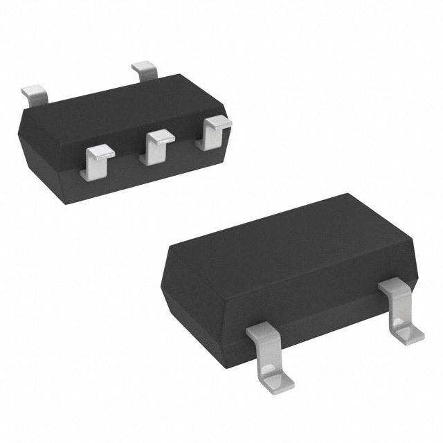
| 描述 | IC REG LDO 1.5V 0.15A SOT23-5低压差稳压器 IC Regulator LN 150MA, 1.5V |
| 产品分类 | |
| 品牌 | STMicroelectronics |
| 产品手册 | |
| 产品图片 |
|
| rohs | 符合RoHS无铅 / 符合限制有害物质指令(RoHS)规范要求 |
| 产品系列 | 电源管理 IC,低压差稳压器,STMicroelectronics LD39015M15R- |
| 数据手册 | |
| 产品型号 | LD39015M15R |
| 产品目录页面 | |
| 产品种类 | 低压差稳压器 |
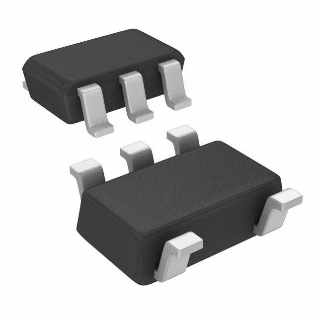
| 供应商器件封装 | SOT-23-5 |
| 其它名称 | 497-6976-1 |
| 其它有关文件 | http://www.st.com/web/catalog/sense_power/FM142/CL1015/SC312/SS1731/PF220700?referrer=70071840 |
| 包装 | 剪切带 (CT) |
| 商标 | STMicroelectronics |
| 回动电压—最大值 | 80 mV |
| 安装类型 | 表面贴装 |
| 安装风格 | SMD/SMT |
| 封装 | Reel |
| 封装/外壳 | SC-74A,SOT-753 |
| 封装/箱体 | SOT-23-5 |
| 工作温度 | -40°C ~ 125°C |
| 工厂包装数量 | 3000 |
| 最大工作温度 | + 125 C |
| 最大输入电压 | 5.5 V |
| 最小工作温度 | - 40 C |
| 最小输入电压 | + 1.5 V |
| 标准包装 | 1 |
| 特色产品 | http://www.digikey.com/cn/zh/ph/ST/LD39015xx.html |
| 电压-跌落(典型值) | 0.08V @ 100mA |
| 电压-输入 | 最高 5.5V |
| 电压-输出 | 1.5V |
| 电压调节准确度 | 2 % |
| 电流-输出 | 150mA |
| 电流-限制(最小值) | - |
| 稳压器拓扑 | 正,固定式 |
| 稳压器数 | 1 |
| 系列 | LD39015 |
| 线路调整率 | 0.01 % / V |
| 负载调节 | 0.002 % / mA |
| 输入偏压电流—最大 | 0.018 mA |
| 输出电压 | 1.5 V |
| 输出电流 | 150 mA |
| 输出端数量 | 1 Output |
| 输出类型 | Fixed |


- 商务部:美国ITC正式对集成电路等产品启动337调查
- 曝三星4nm工艺存在良率问题 高通将骁龙8 Gen1或转产台积电
- 太阳诱电将投资9.5亿元在常州建新厂生产MLCC 预计2023年完工
- 英特尔发布欧洲新工厂建设计划 深化IDM 2.0 战略
- 台积电先进制程称霸业界 有大客户加持明年业绩稳了
- 达到5530亿美元!SIA预计今年全球半导体销售额将创下新高
- 英特尔拟将自动驾驶子公司Mobileye上市 估值或超500亿美元
- 三星加码芯片和SET,合并消费电子和移动部门,撤换高东真等 CEO
- 三星电子宣布重大人事变动 还合并消费电子和移动部门
- 海关总署:前11个月进口集成电路产品价值2.52万亿元 增长14.8%


PDF Datasheet 数据手册内容提取
LD39015 150 mA low quiescent current and low noise voltage regulator Datasheet - production data • Compatible with ceramic capacitors C = 1 µF O • Internal current and thermal limit • Temperature range: -40 °C to 125 °C Description SOT23-5L The LD39015 series provides 150 mA maximum current with an input voltage range from 1.5 V to 5.5 V and a typical dropout voltage of 80 mV. It is stable with ceramic capacitors. The ultra low drop Features voltage, low quiescent current and low noise features make it suitable for low power battery- • Input voltage from 1.5 to 5.5 V powered applications. Power supply rejection is • Ultra low-dropout voltage (80 mV typ. at 100 65 dB at low frequencies and starts rolling off at mA load) 10 kHz. Enable logic control function puts the LD39015 in shutdown mode allowing a total • Very low quiescent current (18 µA typ. at no current consumption lower than 1 µA. The device load, 38 µA typ. at 150 mA load, 1 µA max. in also includes short-circuit constant current limiting OFF mode) and thermal protection. Typical applications are • Very low noise without bypass capacitor mobile phones, personal digital assistants (29µVRMS at VOUT = 0.8 V) (PDAs), cordless phones or similar battery- • Output voltage tolerance: ± 2.0% @ 25 °C powered systems. • 150 mA guaranteed output current • Wide range of output voltages available on request: 0.8 V to 3.3 V with 100 mV step • Logic-controlled electronic shutdown Table 1. Device s ummary Order codes Output voltages LD39015M08R 0.8 V LD39015M10R 1.0 V LD39015M12R 1.2 V LD39015M125R 1.25 V LD39015M15R 1.5 V LD39015M18R 1.8 V LD39015M25R 2.5 V LD39015M33R 3.3 V July 2015 DocID14003 Rev 5 1/15 This is information on a product in full production. www.st.com
Contents LD39015 Contents 1 Diagram . . . . . . . . . . . . . . . . . . . . . . . . . . . . . . . . . . . . . . . . . . . . . . . . . . . 3 2 Pin configuration . . . . . . . . . . . . . . . . . . . . . . . . . . . . . . . . . . . . . . . . . . . . 4 3 Typical application . . . . . . . . . . . . . . . . . . . . . . . . . . . . . . . . . . . . . . . . . . 5 4 Maximum ratings . . . . . . . . . . . . . . . . . . . . . . . . . . . . . . . . . . . . . . . . . . . . 6 5 Electrical characteristics . . . . . . . . . . . . . . . . . . . . . . . . . . . . . . . . . . . . . 7 6 Typical performance characteristics . . . . . . . . . . . . . . . . . . . . . . . . . . . . 9 7 Package information . . . . . . . . . . . . . . . . . . . . . . . . . . . . . . . . . . . . . . . . 11 7.1 SOT23-5L package information . . . . . . . . . . . . . . . . . . . . . . . . . . . . . . . . .11 7.2 SOT23-5L packing information . . . . . . . . . . . . . . . . . . . . . . . . . . . . . . . . . 13 8 Revision history . . . . . . . . . . . . . . . . . . . . . . . . . . . . . . . . . . . . . . . . . . . 14 2/15 DocID14003 Rev 5
LD39015 Diagram 1 Diagram Figure 1. Block diagram IINN OOUUTT BBaannddGGaapp 11..2222 VV RR11 TTrriimmmmiinngg TThheerrmmaall RR22 PPrrootteeccttiioonn EEnnaabbllee EENN GGNNDD DocID14003 Rev 5 3/15 15
Pin configuration LD39015 2 Pin configuration Figure 2. Pin connection (top view) SOT23-5L Table 2. Pin description Pin n° Symbol Function 1 IN LDO input voltage 2 GND Common ground 3 EN Enable pin logic input: low = shutdown, high = active 4 NC Not connected 5 OUT Output voltage 4/15 DocID14003 Rev 5
LD39015 Typical application 3 Typical application Figure 3. Typical application circuit (cid:57)(cid:57) (cid:44)(cid:44)(cid:49)(cid:49) (cid:50)(cid:50)(cid:56)(cid:56)(cid:55)(cid:55) (cid:57)(cid:57) (cid:44)(cid:44)(cid:49)(cid:49) (cid:50)(cid:50)(cid:56)(cid:56)(cid:55)(cid:55) (cid:20)(cid:20)(cid:3)(cid:3)(cid:151)(cid:151)(cid:41)(cid:41) (cid:20)(cid:20)(cid:3)(cid:3)(cid:151)(cid:151)(cid:41)(cid:41) (cid:47)(cid:47)(cid:82)(cid:82)(cid:68)(cid:68)(cid:71)(cid:71) (cid:57)(cid:57) (cid:40)(cid:40)(cid:49)(cid:49) (cid:42)(cid:42)(cid:49)(cid:49)(cid:39)(cid:39) (cid:40)(cid:40)(cid:49)(cid:49) DocID14003 Rev 5 5/15 15
Maximum ratings LD39015 4 Maximum ratings Table 3. Absolute maximum ratings Symbol Parameter Value Unit V DC input voltage -0.3 to 7 V IN V DC output voltage - 0.3 to V + 0.3 V OUT I V Enable input voltage - 0.3 to V + 0.3 V EN I I Output current Internally limited mA OUT P Power dissipation Internally limited mW D T Storage temperature range -65 to 150 °C STG T Operating junction temperature range -40 to 125 °C OP Note: Absolute maximum ratings are those values beyond which damage to the device may occur. Functional operation under these conditions is not implied. All values are referred to GND. Table 4. Thermal data Symbol Parameter SOT23-5L Unit R Thermal resistance junction-ambient 255 °C/W thJA R Thermal resistance junction-case 81 °C/W thJC 6/15 DocID14003 Rev 5
LD39015 Electrical characteristics 5 Electrical characteristics T = 25 °C, V = V + 1 V, C = C = 1 µF, I = 1 mA, V = V , unless J IN OUT(NOM) IN OUT OUT EN IN otherwise specified. Table 5. Electrical characteristics(1) Symbol Parameter Test conditions Min. Typ. Max. Unit V Operating input voltage 1.5 5.5 V IN Turn-on threshold 1.45 1.48 V V UVLO Turn-off threshold 1.30 1.35 mV V > 1.5 V, I = 1 mA OUT OUT -2.0 2.0 T = 25 °C J % V > 1.5 V, I = 1 mA OUT OUT -3.0 3.0 VOUT VOUT accuracy -40 °C < TJ < 125 °C V ≤ 1.5 V, I = 1 mA ±10 OUT OUT V ≤ 1.5 V, I = 1 mA mV OUT OUT ±30 -40 °C < T < 125 °C J V +1 V ≤ V ≤ 5.5 V ΔV Static line regulation OUT IN 0.01 %/V OUT I = 1 mA OUT ΔV = + 500 mV, I = 1 mA ΔV Transient line regulation (2) IN OUT 10 mVpp OUT T = T = 5 µs R F ΔV Static load regulation I = 1 mA to 150 mA 0.002 %/mA OUT OUT I = 1 mA to 150 mA ΔV Transient load regulation (2) OUT 40 mVpp OUT T = T = 5 µs R F I = 100 mA, V > 1.5 V V Dropout voltage (3) OUT OUT 80 100 mV DROP -40 °C < T < 125 °C J 1.1 kHz to 100 kHz, I = 10 mA e Output noise voltage OUT 29 µV N V = 0.8 V RMS OUT V = V + 0.5 V +/-V IN OUTNOM RIPPLE VRIPPLE = 0.1 V, freq. = 1 kHz 65 Supply voltage rejection IOUT = 10 mA SVR dB VOUT = 1.5 V VIN = VOUTNOM + 0.5 V +/-VRIPPLE VRIPPLE = 0.1 V, freq.=10 kHz 62 I = 10 mA OUT I = 0 mA 18 OUT I = 0 mA, -40 °C < T < 125 °C 50 OUT J I = 0 to 150 mA 38 OUT I Quiescent current µA Q I = 0 to 150 mA OUT 70 -40 °C < T < 125 °C J V input current in OFF mode: IN 0.001 1 V = GND EN DocID14003 Rev 5 7/15 15
Electrical characteristics LD39015 Table 5. Electrical characteristics (continued)(1) Symbol Parameter Test conditions Min. Typ. Max. Unit I Short-circuit current R = 0 350 mA SC L V = 1.5 V to 5.5 V Enable input logic low IN 0.4 V -40 °C < T < 125 °C J V EN V = 1.5 V to 5.5 V Enable input logic high IN 0.9 V -40 °C < T < 125 °C J I Enable pin input current V = V 0.1 100 nA EN EN IN T Turn-on time (4) 30 µs ON Thermal shutdown 160 T °C SHDN Hysteresis 20 Capacitance (see typical C Output capacitor performance characteristics for 1 22 µF OUT stability) 1. For V < 1.2 V, V = 1.5 V OUT(NOM) IN 2. All transient values are guaranteed by design, not production tested 3. Dropout voltage is the input-to-output voltage difference at which the output voltage is 100 mV below its nominal value. This specification does not apply to output voltages below 1.5 V 4. Turn-on time is the time measured between the enable input just exceeding V high value and the output voltage just EN reaching 95% of its nominal value 8/15 DocID14003 Rev 5
LD39015 Typical performance characteristics 6 Typical performance characteristics Figure 4. Output voltage vs. temperature Figure 5. Output voltage vs. input voltage 00..8855 00..8844 II ==11mmAA (cid:19)(cid:19)(cid:17)(cid:17)(cid:28)(cid:28) OOUUTT 00..8833 (cid:19)(cid:19)(cid:17)(cid:17)(cid:27)(cid:27) II ==110000mmAA OOUUTT (cid:19)(cid:19)(cid:17)(cid:17)(cid:26)(cid:26) 00..8822 (cid:19)(cid:19)(cid:17)(cid:17)(cid:25)(cid:25) ]] 00..8811 [V[VTT 00..88 (cid:62)(cid:57)(cid:64)(cid:62)(cid:57)(cid:64)(cid:55)(cid:55) (cid:19)(cid:19)(cid:17)(cid:17)(cid:24)(cid:24) UU (cid:56)(cid:56) (cid:19)(cid:19)(cid:17)(cid:17)(cid:23)(cid:23) OO 00..7799 (cid:50)(cid:50) VV (cid:57)(cid:57) (cid:19)(cid:19)(cid:17)(cid:17)(cid:22)(cid:22) 00..7788 (cid:19)(cid:19)(cid:17)(cid:17)(cid:21)(cid:21) 00..7777 (cid:19)(cid:19)(cid:17)(cid:17)(cid:20)(cid:20) 00..7766 VV ==11..55VV IINN (cid:19)(cid:19) 00..7755 (cid:19)(cid:19) (cid:20)(cid:20) (cid:21)(cid:21) (cid:22)(cid:22) (cid:23)(cid:23) (cid:24)(cid:24) (cid:25)(cid:25) --5500 00 5500 110000 115500 (cid:57)(cid:57) (cid:62)(cid:62)(cid:57)(cid:57)(cid:64)(cid:64) (cid:44)(cid:44)(cid:49)(cid:49) TTeemmpp [[°°CC]] Figure 6. Dropout voltage vs. output current Figure 7. C stability region OUT 22..44 00..1166 CC ==11 µµFF,, VV ==VV ==11..55 ttoo 55..55 VV II ==11 mmAAttoo 00..1155 AA m]m] 22..11 IINN IINN EENN OOUUTT 00..1144 hh 00..1122 OO 11..88 V]V] z [z [ [[ 00..11 HH 11..55 utut KK oo 00..0088 0 0 11..22 pp 00 SSTTAABBIILLIITTYY RREEGGIIOONN oo 00..0066 11 drdr @ @ 00..99 VV 00..0044 R R 00..66 00..0022 SS EE 00..33 00 00 00..0055 00..11 00..1155 00..22 00..2255 00 00 55 1100 1155 2200 2255 II [[AA]] OOUUTT CC [[µµFF]] ((nnoommiinnaall vvaalluuee)) OOUUTT Figure 8. Supply voltage rejection vs. frequency Figure 9. Output noise voltage vs. frequency 7755 880000 II ==1100 mmAA,, VV ==44..33 VV,, CC ==CC == 11µµFF 7700 OOUUTT IINN IINN OOUUTT 770000 6655 VV ==33..33 VV 6600 660000 OOUUTT 5555 B]B] 5500 550000 R [dR [d 44440505 HzHz 440000 SVSV 3355 √√V/V/ 330000 3300 nn 2255 II == 1100mmAA VVrriippppllee== 00..11VVpppp 220000 2200 OOUUTT 1155 110000 1100 00 110000 11000000 1100000000 110000000000 11000000 1100000000 110000000000 FFrreeqq [[HHzz]] FFRREEQQ [[HHzz]] DocID14003 Rev 5 9/15 15
Typical performance characteristics LD39015 Figure 10. Quiescent current vs. input voltage Figure 11. Load transient 110000 8800 A]A]6600 µµ [[ qq4400 II 2200 VV ==VV ,, CC ==CC ==11µµFF,, II ==00..1155AA IINN IINNHH IINN OOUUTT OOUUTT 00 11..44 11..99 22..44 22..99 33..44 33..99 44..44 44..99 55..44 55..99 VV [[VV]] IINN V = V = 1.5V, I = 1mA to 0.15A, C = C = 1µF, EN IN OUT IN OUT t = t = 5µs r f Figure 12. Line transient Figure 13. Enable transient VIN = VEN = 1.5 to 5.5V, IOUT = 1mA, COUT = 1µF, VIN = 1.5V, VEN = 0 to 1V, IOUT = 1mA, CIN = COUT = 1µF t = t = 5µs r f 10/15 DocID14003 Rev 5
LD39015 Package information 7 Package information In order to meet environmental requirements, ST offers these devices in different grades of ECOPACK® packages, depending on their level of environmental compliance. ECOPACK® specifications, grade definitions and product status are available at: www.st.com. ECOPACK is an ST trademark. 7.1 SOT23-5L package information Figure 14. SOT23-5L package outline (cid:26)(cid:19)(cid:23)(cid:28)(cid:25)(cid:26)(cid:25)(cid:66)(cid:78) DocID14003 Rev 5 11/15 15
Package information LD39015 Table 6. SOT23-5L mechanical data mm Dim. Min. Typ. Max. A 0.90 1.45 A1 0 0.15 A2 0.90 1.30 b 0.30 0.50 c 0.09 0.20 D 2.95 E 1.60 e 0.95 H 2.80 L 0.30 0.60 q 0 8 Figure 15. SOT23-5L recommended footprint (dimensions in mm) (cid:26)(cid:19)(cid:23)(cid:28)(cid:25)(cid:26)(cid:25)(cid:66)(cid:78) 12/15 DocID14003 Rev 5
LD39015 Package information 7.2 SOT23-5L packing information Figure 16. SOT23-5L tape and reel outline Table 7. SOT23-5L tape and reel mechanical data mm Dim. Min. Typ. Max. A 180 C 12.8 13.0 13.2 D 20.2 N 60 T 14.4 Ao 3.13 3.23 3.33 Bo 3.07 3.17 3.27 Ko 1.27 1.37 1.47 Po 3.9 4.0 4.1 P 3.9 4.0 4.1 DocID14003 Rev 5 13/15 15
Revision history LD39015 8 Revision history Table 8. Document revision history Date Revision Changes 13-Nov-2007 1 Initial release. 11-Apr-2008 2 Modified: Table5 on page7. 12-Feb-2009 3 Modified: Table1 on page1. Part number LD39015xx changed to LD39015. Updated the Description in cover page and Section7: Package information. 11-Feb-2014 4 Added Section7.2: SOT23-5L packing information. Minor text changes. Removed SOT666 package. Updated features in cover page, Table1: Device summary, Table2: Pin 07-Jul-2015 5 description, Table4: Thermal data, Figure2: Pin connection (top view) and Section7: Package information. Minor text changes. 14/15 DocID14003 Rev 5
LD39015 IMPORTANT NOTICE – PLEASE READ CAREFULLY STMicroelectronics NV and its subsidiaries (“ST”) reserve the right to make changes, corrections, enhancements, modifications, and improvements to ST products and/or to this document at any time without notice. Purchasers should obtain the latest relevant information on ST products before placing orders. ST products are sold pursuant to ST’s terms and conditions of sale in place at the time of order acknowledgement. Purchasers are solely responsible for the choice, selection, and use of ST products and ST assumes no liability for application assistance or the design of Purchasers’ products. No license, express or implied, to any intellectual property right is granted by ST herein. Resale of ST products with provisions different from the information set forth herein shall void any warranty granted by ST for such product. ST and the ST logo are trademarks of ST. All other product or service names are the property of their respective owners. Information in this document supersedes and replaces information previously supplied in any prior versions of this document. © 2015 STMicroelectronics – All rights reserved DocID14003 Rev 5 15/15 15
Mouser Electronics Authorized Distributor Click to View Pricing, Inventory, Delivery & Lifecycle Information: S TMicroelectronics: LD39015M12R LD39015M10R LD39015M08R LD39015M15R LD39015M18R LD39015M25R LD39015M33R LD39015M125R LD39015XG08R LD39015XG10R