ICGOO在线商城 > 集成电路(IC) > PMIC - 稳压器 - 线性 > LD1117DT25TR
 Datasheet下载
- 型号: LD1117DT25TR
- 制造商: STMicroelectronics
- 库位|库存: xxxx|xxxx
- 要求:
| 数量阶梯 | 香港交货 | 国内含税 |
| +xxxx | $xxxx | ¥xxxx |
查看当月历史价格
查看今年历史价格
LD1117DT25TR产品简介:
ICGOO电子元器件商城为您提供LD1117DT25TR由STMicroelectronics设计生产,在icgoo商城现货销售,并且可以通过原厂、代理商等渠道进行代购。 LD1117DT25TR价格参考¥1.56-¥1.56。STMicroelectronicsLD1117DT25TR封装/规格:PMIC - 稳压器 - 线性, Linear Voltage Regulator IC Positive Fixed 1 Output 2.5V 800mA DPAK。您可以下载LD1117DT25TR参考资料、Datasheet数据手册功能说明书,资料中有LD1117DT25TR 详细功能的应用电路图电压和使用方法及教程。
STMicroelectronics的LD1117DT25TR是一款PMIC(电源管理集成电路)中的线性稳压器,具有以下典型应用场景:

 1. 低功耗电子设备
   - LD1117DT25TR适用于需要稳定电压输出的低功耗设备。其固定输出电压为2.5V,能够为各种小型电子设备供电,例如手持式设备、传感器模块和便携式医疗设备。

 2. 嵌入式系统
   - 在嵌入式系统中,该稳压器可以为微控制器、数字信号处理器(DSP)或其他低功耗芯片提供稳定的电源支持。它具有较低的压差(Dropout Voltage),适合对电源效率要求较高的应用。

 3. 物联网(IoT)设备
   - IoT设备通常需要长时间运行且功耗较低。LD1117DT25TR的高精度输出电压和良好的热稳定性使其成为无线传感器节点、智能家庭设备和可穿戴设备的理想选择。

 4. 音频设备
   - 由于其低噪声特性,LD1117DT25TR可用于音频放大器或耳机放大器等对电源质量要求较高的场景,确保音频信号的纯净度。

 5. 电池供电设备
   - 对于由电池供电的设备,如遥控器、电子玩具或便携式仪器,LD1117DT25TR的高效能和稳定性可以延长电池使用寿命。

 6. 工业控制
   - 在工业自动化领域,该稳压器可用于为传感器、执行器和其他低功耗组件供电,确保系统的可靠性和稳定性。

 特性总结
- 输入电压范围:2.7V至13.8V
- 输出电流:高达800mA
- 封装形式:TO-220,便于散热
- 工作温度范围:-40°C至125°C,适应多种环境条件

总之,LD1117DT25TR以其高可靠性、低功耗和宽泛的工作范围,广泛应用于消费电子、工业控制和物联网等领域。
| 参数 | 数值 |
| 产品目录 | 集成电路 (IC)半导体 |
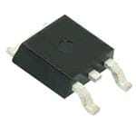
| 描述 | IC REG LDO 2.5V 0.8A DPAK低压差稳压器 2.5V 0.8A Positive |
| 产品分类 | |
| 品牌 | STMicroelectronics |
| 产品手册 | |
| 产品图片 |
|
| rohs | 符合RoHS无铅 / 符合限制有害物质指令(RoHS)规范要求 |
| 产品系列 | 电源管理 IC,低压差稳压器,STMicroelectronics LD1117DT25TR- |
| 数据手册 | |
| 产品型号 | LD1117DT25TR |
| 产品目录页面 | |
| 产品种类 | 低压差稳压器 |
| 供应商器件封装 | D-Pak |
| 其它名称 | 497-7307-6 |
| 其它有关文件 | http://www.st.com/web/catalog/sense_power/FM142/CL1015/SC312/PF63472?referrer=70071840 |
| 包装 | Digi-Reel® |
| 商标 | STMicroelectronics |
| 回动电压—最大值 | 1.1 V |
| 安装类型 | 表面贴装 |
| 安装风格 | SMD/SMT |
| 封装 | Reel |
| 封装/外壳 | TO-252-3,DPak(2 引线+接片),SC-63 |
| 封装/箱体 | TO-252 |
| 工作温度 | 0°C ~ 125°C |
| 工厂包装数量 | 2500 |
| 最大功率耗散 | 12 W |
| 最大工作温度 | + 150 C |
| 最大输入电压 | 15 V |
| 最小工作温度 | 0 C |
| 标准包装 | 1 |
| 电压-跌落(典型值) | 1.1V @ 800mA |
| 电压-输入 | 最高 15V |
| 电压-输出 | 2.5V |
| 电压调节准确度 | 1 % |
| 电流-输出 | 800mA |
| 电流-限制(最小值) | - |
| 稳压器拓扑 | 正,固定式 |
| 稳压器数 | 1 |
| 系列 | LD1117DT2 |
| 线路调整率 | 6 mV |
| 负载调节 | 10 mV |
| 输入偏压电流—最大 | 5 mA |
| 输出电压 | 2.5 V |
| 输出电流 | 950 mA |
| 输出端数量 | 1 Output |
| 输出类型 | Fixed |


- 商务部:美国ITC正式对集成电路等产品启动337调查
- 曝三星4nm工艺存在良率问题 高通将骁龙8 Gen1或转产台积电
- 太阳诱电将投资9.5亿元在常州建新厂生产MLCC 预计2023年完工
- 英特尔发布欧洲新工厂建设计划 深化IDM 2.0 战略
- 台积电先进制程称霸业界 有大客户加持明年业绩稳了
- 达到5530亿美元!SIA预计今年全球半导体销售额将创下新高
- 英特尔拟将自动驾驶子公司Mobileye上市 估值或超500亿美元
- 三星加码芯片和SET,合并消费电子和移动部门,撤换高东真等 CEO
- 三星电子宣布重大人事变动 还合并消费电子和移动部门
- 海关总署:前11个月进口集成电路产品价值2.52万亿元 增长14.8%


PDF Datasheet 数据手册内容提取
LD1117 Adjustable and fixed low drop positive voltage regulator Datasheet - production data flows mostly into the load. Only a very common 10 µF minimum capacitor is needed for stability. On chip trimming allows the regulator to reach a very tight output voltage tolerance, within ± 1 % at 25 °C. The adjustable LD1117 is pin to pin DPAK compatible with the other standard. Adjustable voltage regulators maintaining the better TO-220 performances in terms of drop and tolerance. SOT-223 SO-8 Features • Low dropout voltage (1 V typ.) • 2.85 V device performances are suitable for SCSI-2 active termination • Output current up to 800 mA • Fixed output voltage of: 1.2 V, 1.8 V, 2.5 V, 3.3V, 5.0 V • Adjustable version availability (V = 1.25 V) REF • Internal current and thermal limit • Available in ± 1 % (at 25 °C) and 2 % in full temperature range • Supply voltage rejection: 75 dB (typ.) Description The LD1117 is a low drop voltage regulator able to provide up to 800 mA of output current, available even in adjustable version (V = REF 1.25V). Concerning fixed versions, are offered the following output voltages: 1.2 V, 1.8 V, 2.5 V, 2.85 V, 3.3 V and 5.0 V. The device is supplied in: SOT-223, DPAK, SO-8 and TO-220. The SOT- 223 and DPAK surface mount packages optimize the thermal characteristics even offering a relevant space saving effect. High efficiency is assured by NPN pass transistor. In fact in this case, unlike than PNP one, the quiescent current November 2013 DocID2572 Rev 33 1/44 This is information on a product in full production. www.st.com 44
Contents LD1117 Contents 1 Diagram . . . . . . . . . . . . . . . . . . . . . . . . . . . . . . . . . . . . . . . . . . . . . . . . . . . 5 2 Pin configuration . . . . . . . . . . . . . . . . . . . . . . . . . . . . . . . . . . . . . . . . . . . 6 3 Maximum ratings . . . . . . . . . . . . . . . . . . . . . . . . . . . . . . . . . . . . . . . . . . . . 7 4 Schematic application . . . . . . . . . . . . . . . . . . . . . . . . . . . . . . . . . . . . . . . 8 5 Electrical characteristics . . . . . . . . . . . . . . . . . . . . . . . . . . . . . . . . . . . . . 9 6 Typical application . . . . . . . . . . . . . . . . . . . . . . . . . . . . . . . . . . . . . . . . . 21 7 LD1117 adjustable: application note . . . . . . . . . . . . . . . . . . . . . . . . . . . 24 8 Package mechanical data . . . . . . . . . . . . . . . . . . . . . . . . . . . . . . . . . . . . 25 9 Packing mechanical data . . . . . . . . . . . . . . . . . . . . . . . . . . . . . . . . . . . . 36 10 Order codes . . . . . . . . . . . . . . . . . . . . . . . . . . . . . . . . . . . . . . . . . . . . . . . 42 11 Revision history . . . . . . . . . . . . . . . . . . . . . . . . . . . . . . . . . . . . . . . . . . . 43 2/44 DocID2572 Rev 33
LD1117 List of tables List of tables Table 1. Absolute maximum ratings. . . . . . . . . . . . . . . . . . . . . . . . . . . . . . . . . . . . . . . . . . . . . . . . . . 7 Table 2. Thermal data. . . . . . . . . . . . . . . . . . . . . . . . . . . . . . . . . . . . . . . . . . . . . . . . . . . . . . . . . . . . . 7 Table 3. Electrical characteristics of LD1117#12 . . . . . . . . . . . . . . . . . . . . . . . . . . . . . . . . . . . . . . . . 9 Table 4. Electrical characteristics of LD1117#18 . . . . . . . . . . . . . . . . . . . . . . . . . . . . . . . . . . . . . . . 10 Table 5. Electrical characteristics of LD1117#25 . . . . . . . . . . . . . . . . . . . . . . . . . . . . . . . . . . . . . . . 11 Table 6. Electrical characteristics of LD1117#33 . . . . . . . . . . . . . . . . . . . . . . . . . . . . . . . . . . . . . . . 12 Table 7. Electrical characteristics of LD1117#50 . . . . . . . . . . . . . . . . . . . . . . . . . . . . . . . . . . . . . . . 13 Table 8. Electrical characteristics of LD1117 (adjustable) . . . . . . . . . . . . . . . . . . . . . . . . . . . . . . . . 14 Table 9. Electrical characteristics of LD1117#12C. . . . . . . . . . . . . . . . . . . . . . . . . . . . . . . . . . . . . . 15 Table 10. Electrical characteristics of LD1117#18C. . . . . . . . . . . . . . . . . . . . . . . . . . . . . . . . . . . . . . 16 Table 11. Electrical characteristics of LD1117#25C. . . . . . . . . . . . . . . . . . . . . . . . . . . . . . . . . . . . . . 17 Table 12. Electrical characteristics of LD1117#33C. . . . . . . . . . . . . . . . . . . . . . . . . . . . . . . . . . . . . . 18 Table 13. Electrical characteristics of LD1117#50C. . . . . . . . . . . . . . . . . . . . . . . . . . . . . . . . . . . . . . 19 Table 14. Electrical characteristics of LD1117C (adjustable). . . . . . . . . . . . . . . . . . . . . . . . . . . . . . . 20 Table 15. TO-220 mechanical data (type STD-ST Dual Gauge) . . . . . . . . . . . . . . . . . . . . . . . . . . . . 25 Table 16. TO-220 mechanical data (type STD-ST Single Gauge) . . . . . . . . . . . . . . . . . . . . . . . . . . . 27 Table 17. SOT-223 mechanical data . . . . . . . . . . . . . . . . . . . . . . . . . . . . . . . . . . . . . . . . . . . . . . . . . 29 Table 18. SO-8 mechanical data . . . . . . . . . . . . . . . . . . . . . . . . . . . . . . . . . . . . . . . . . . . . . . . . . . . . 30 Table 19. DPAK mechanical data. . . . . . . . . . . . . . . . . . . . . . . . . . . . . . . . . . . . . . . . . . . . . . . . . . . . 31 Table 20. Footprint data . . . . . . . . . . . . . . . . . . . . . . . . . . . . . . . . . . . . . . . . . . . . . . . . . . . . . . . . . . . 35 Table 21. SOT-223 tape and reel mechanical data . . . . . . . . . . . . . . . . . . . . . . . . . . . . . . . . . . . . . . 37 Table 22. SO-8 tape and reel mechanical data . . . . . . . . . . . . . . . . . . . . . . . . . . . . . . . . . . . . . . . . . 39 Table 23. DPAK tape and reel mechanical data. . . . . . . . . . . . . . . . . . . . . . . . . . . . . . . . . . . . . . . . . 40 Table 24. Order codes . . . . . . . . . . . . . . . . . . . . . . . . . . . . . . . . . . . . . . . . . . . . . . . . . . . . . . . . . . . . 42 Table 25. Document revision history . . . . . . . . . . . . . . . . . . . . . . . . . . . . . . . . . . . . . . . . . . . . . . . . . 43 DocID2572 Rev 33 3/44
List of figures LD1117 List of figures Figure 1. Block diagram. . . . . . . . . . . . . . . . . . . . . . . . . . . . . . . . . . . . . . . . . . . . . . . . . . . . . . . . . . . . 5 Figure 2. Pin connections (top view) . . . . . . . . . . . . . . . . . . . . . . . . . . . . . . . . . . . . . . . . . . . . . . . . . . 6 Figure 3. Application circuit (for 1.2 V). . . . . . . . . . . . . . . . . . . . . . . . . . . . . . . . . . . . . . . . . . . . . . . . . 8 Figure 4. Application circuit (for other fixed output voltages). . . . . . . . . . . . . . . . . . . . . . . . . . . . . . . . 8 Figure 5. Negative supply . . . . . . . . . . . . . . . . . . . . . . . . . . . . . . . . . . . . . . . . . . . . . . . . . . . . . . . . . 21 Figure 6. Circuit for increasing output voltage. . . . . . . . . . . . . . . . . . . . . . . . . . . . . . . . . . . . . . . . . . 21 Figure 7. Voltage regulator with reference. . . . . . . . . . . . . . . . . . . . . . . . . . . . . . . . . . . . . . . . . . . . . 21 Figure 8. Battery backed-up regulated supply. . . . . . . . . . . . . . . . . . . . . . . . . . . . . . . . . . . . . . . . . . 22 Figure 9. Post-regulated dual supply. . . . . . . . . . . . . . . . . . . . . . . . . . . . . . . . . . . . . . . . . . . . . . . . . 23 Figure 10. Adjustable output voltage application. . . . . . . . . . . . . . . . . . . . . . . . . . . . . . . . . . . . . . . . . 24 Figure 11. Adjustable output voltage application with improved ripple rejection . . . . . . . . . . . . . . . . . 24 Figure 12. Drawing dimension TO-220 (type STD-ST Dual Gauge) . . . . . . . . . . . . . . . . . . . . . . . . . . 26 Figure 13. Drawing dimension TO-220 (type STD-ST Single Gauge). . . . . . . . . . . . . . . . . . . . . . . . . 28 Figure 14. Drawing dimension SOT-223 . . . . . . . . . . . . . . . . . . . . . . . . . . . . . . . . . . . . . . . . . . . . . . . 29 Figure 15. Drawing dimension SO-8 . . . . . . . . . . . . . . . . . . . . . . . . . . . . . . . . . . . . . . . . . . . . . . . . . . 30 Figure 16. Drawing dimension DPAK (type STD-ST) . . . . . . . . . . . . . . . . . . . . . . . . . . . . . . . . . . . . . 32 Figure 17. Drawing dimension DPAK (type Fujitsu-subcon.). . . . . . . . . . . . . . . . . . . . . . . . . . . . . . . . 33 Figure 18. Drawing dimension DPAK (type IDS-subcon.) . . . . . . . . . . . . . . . . . . . . . . . . . . . . . . . . . . 34 Figure 19. DPAK footprint recommended data . . . . . . . . . . . . . . . . . . . . . . . . . . . . . . . . . . . . . . . . . . 35 Figure 20. Drawing dimension tube for TO-220 Dual Gauge (mm.) . . . . . . . . . . . . . . . . . . . . . . . . . . 36 Figure 21. Drawing dimension tube for TO-220 Single Gauge (mm.) . . . . . . . . . . . . . . . . . . . . . . . . . 36 Figure 22. Tape for SOT-223 (dimensions are in mm) . . . . . . . . . . . . . . . . . . . . . . . . . . . . . . . . . . . . 37 Figure 23. Reel for STO-223 (dimensions are in mm). . . . . . . . . . . . . . . . . . . . . . . . . . . . . . . . . . . . . 38 Figure 24. SO-8 tape and reel dimensions . . . . . . . . . . . . . . . . . . . . . . . . . . . . . . . . . . . . . . . . . . . . . 39 Figure 25. DPAK footprint . . . . . . . . . . . . . . . . . . . . . . . . . . . . . . . . . . . . . . . . . . . . . . . . . . . . . . . . . . 40 Figure 26. Tape for DPAK . . . . . . . . . . . . . . . . . . . . . . . . . . . . . . . . . . . . . . . . . . . . . . . . . . . . . . . . . . 41 Figure 27. Reel for DPAK . . . . . . . . . . . . . . . . . . . . . . . . . . . . . . . . . . . . . . . . . . . . . . . . . . . . . . . . . . 41 4/44 DocID2572 Rev 33
LD1117 Diagram 1 Diagram Figure 1. Block diagram DocID2572 Rev 33 5/44
Pin configuration LD1117 2 Pin configuration Figure 2. Pin connections (top view) SO-8 SOT-223 DPAK TO-220 Note: The TAB is connected to the V . OUT 6/44 DocID2572 Rev 33
LD1117 Maximum ratings 3 Maximum ratings Table 1. Absolute maximum ratings Symbol Parameter Value Unit V (1) DC input voltage 15 V IN P Power dissipation 12 W TOT T Storage temperature range -40 to +150 °C STG for C version -40 to +125 °C T Operating junction temperature range OP for standard version 0 to +125 °C 1. Absolute maximum rating of V = 18 V, when I is lower than 20 mA. IN OUT Table 2. Thermal data Symbol Parameter SOT-223 SO-8 DPAK TO-220 Unit R Thermal resistance junction-case 15 20 8 5 °C/W thJC R Thermal resistance junction-ambient 110 55 100 50 °C/W thJA DocID2572 Rev 33 7/44
Schematic application LD1117 4 Schematic application Figure 3. Application circuit (for 1.2 V) Figure 4. Application circuit (for other fixed output voltages) 8/44 DocID2572 Rev 33
LD1117 Electrical characteristics 5 Electrical characteristics Refer to the test circuits, T = 0 to 125 °C, C = 10 µF, R = 120 Ω between GND and OUT J O pins, unless otherwise specified. Table 3. Electrical characteristics of LD1117#12 Symbol Parameter Test condition Min. Typ. Max. Unit V Output voltage V = 3.2 V, I = 10 mA, T = 25 °C 1.188 1.20 1.212 V O in O J I = 10 to 800 mA V Output voltage O 1.140 1.20 1.260 V O V - V = 1.4 to 10 V in O ΔV Line regulation V - V = 1.5 to 13.75 V, I = 10 mA 0.035 0.2 % O in O O ΔV Load regulation V - V = 3 V, I = 10 to 800 mA 0.1 0.4 % O in O O ΔV Temperature stability 0.5 % O ΔV Long term stability 1000 hrs, T = 125 °C 0.3 % O J V Operating input voltage 15 V in I Adjustment pin current V ≤ 15 V 60 120 µA adj in V - V = 1.4 to 10 V ΔI Adjustment pin current change in O 1 5 µA adj I = 10 to 800 mA O I Minimum load current V = 15 V 2 5 mA O(min) in I Output current V - V = 5 V, T = 25 °C 800 950 1300 mA O in O J eN Output noise (%V ) B = 10 Hz to 10 kHz, T = 25 °C 0.003 % O J I = 40 mA, f = 120 Hz, T = 25 °C SVR Supply voltage rejection O J 60 75 dB V - V = 3 V, V = 1 V in O ripple PP I = 100 mA 1 1.1 O V Dropout voltage I = 500 mA 1.05 1.15 V d O I = 800 mA 1.10 1.2 O Thermal regulation T = 25 °C, 30 ms Pulse 0.01 0.1 %/W a DocID2572 Rev 33 9/44
Electrical characteristics LD1117 Refer to the test circuits, T = 0 to 125 °C, C = 10 µF, unless otherwise specified. J O Table 4. Electrical characteristics of LD1117#18 Symbol Parameter Test condition Min. Typ. Max. Unit V Output voltage V = 3.8 V, I = 10 mA, T = 25 °C 1.78 1.8 1.82 V O in O J V Output voltage I = 0 to 800 mA, V = 3.3 to 8 V 1.76 1.84 V O O in ΔV Line regulation V = 3.3 to 8 V, I = 0 mA 1 6 mV O in O ΔV Load regulation V = 3.3 V, I = 0 to 800 mA 1 10 mV O in O ΔV Temperature stability 0.5 % O ΔV Long term stability 1000 hrs, T = 125 °C 0.3 % O J V Operating input voltage I = 100 mA 15 V in O I Quiescent current V ≤ 8 V 5 10 mA d in I Output current V = 6.8 V, T = 25 °C 800 950 1300 mA O in J eN Output noise voltage B = 10 Hz to 10 kHz, T = 25 °C 100 µV J I = 40 mA, f = 120 Hz, T = 25 °C SVR Supply voltage rejection O J 60 75 dB V = 5.5 V, V = 1 V in ripple PP I = 100 mA 1 1.1 O V Dropout voltage I = 500 mA 1.05 1.15 V d O I = 800 mA 1.10 1.2 O Thermal regulation T = 25 °C, 30 ms Pulse 0.01 0.1 %/W a 10/44 DocID2572 Rev 33
LD1117 Electrical characteristics Refer to the test circuits, T = 0 to 125 °C, C = 10 µF, unless otherwise specified. J O Table 5. Electrical characteristics of LD1117#25 Symbol Parameter Test condition Min. Typ. Max. Unit V Output voltage V = 4.5 V, I = 10 mA, T = 25 °C 2.475 2.5 2.525 V O in O J V Output voltage I = 0 to 800 mA, V = 3.9 to 10 V 2.45 2.55 V O O in ΔV Line regulation V = 3.9 to 10 V, I = 0 mA 1 6 mV O in O ΔV Load regulation V = 3.9 V, I = 0 to 800 mA 1 10 mV O in O ΔV Temperature stability 0.5 % O ΔV Long term stability 1000 hrs, T = 125 °C 0.3 % O J V Operating input voltage I = 100 mA 15 V in O I Quiescent current V ≤ 10 V 5 10 mA d in I Output current V = 7.5 V T = 25 °C 800 950 1300 mA O in J eN Output noise voltage B = 10 Hz to 10 kHz, T = 25 °C 100 µV J I = 40 mA, f = 120 Hz, T = 25 °C SVR Supply voltage rejection O J 60 75 dB V = 5.5 V, V = 1 V in ripple PP I = 100 mA 1 1.1 O V Dropout voltage I = 500 mA 1.05 1.15 V d O I = 800 mA 1.10 1.2 O Thermal regulation T = 25 °C, 30 ms Pulse 0.01 0.1 %/W a DocID2572 Rev 33 11/44
Electrical characteristics LD1117 Refer to the test circuits, T = 0 to 125 °C, C = 10 µF, unless otherwise specified. J O Table 6. Electrical characteristics of LD1117#33 Symbol Parameter Test condition Min. Typ. Max. Unit V Output voltage V = 5.3 V, I = 10 mA, T = 25 °C 3.267 3.3 3.333 V O in O J V Output voltage I = 0 to 800 mA, V = 4.75 to 10 V 3.235 3.365 V O O in ΔV Line regulation V = 4.75 to 15 V, I = 0 mA 1 6 mV O in O ΔV Load regulation V = 4.75 V, I = 0 to 800 mA 1 10 mV O in O ΔV Temperature stability 0.5 % O ΔV Long term stability 1000 hrs, T = 125 °C 0.3 % O J V Operating input voltage I = 100 mA 15 V in O I Quiescent current V ≤ 15 V 5 10 mA d in I Output current V = 8.3 V, T = 25 °C 800 950 1300 mA O in J eN Output noise voltage B = 10 Hz to 10 kHz, T = 25 °C 100 µV J I = 40 mA, f = 120 Hz, T = 25 °C SVR Supply voltage rejection O J 60 75 dB V = 6.3 V, V = 1 V in ripple PP I = 100 mA 1 1.1 O V Dropout voltage I = 500 mA 1.05 1.15 V d O I = 800 mA 1.10 1.2 O Thermal regulation T = 25 °C, 30 ms Pulse 0.01 0.1 %/W a 12/44 DocID2572 Rev 33
LD1117 Electrical characteristics Refer to the test circuits, T = 0 to 125 °C, C = 10 µF, unless otherwise specified. J O Table 7. Electrical characteristics of LD1117#50 Symbol Parameter Test condition Min. Typ. Max. Unit V Output voltage V = 7 V, I = 10 mA, T = 25 °C 4.95 5 5.05 V O in O J V Output voltage I = 0 to 800 mA, V = 6.5 to 15 V 4.9 5.1 V O O in ΔV Line regulation V = 6.5 to 15 V, I = 0 mA 1 10 mV O in O ΔV Load regulation V = 6.5 V, I = 0 to 800 mA 1 15 mV O in O ΔV Temperature stability 0.5 % O ΔV Long term stability 1000 hrs, T = 125 °C 0.3 % O J V Operating input voltage I = 100 mA 15 V in O I Quiescent current V ≤ 15 V 5 10 mA d in I Output current V = 10 V, T = 25 °C 800 950 1300 mA O in J eN Output noise voltage B = 10 Hz to 10 kHz, T = 25 °C 100 µV J I = 40 mA, f = 120 Hz, T = 25 °C SVR Supply voltage rejection O J 60 75 dB V = 8 V, V = 1 V in ripple PP I = 100 mA 1 1.1 O V Dropout voltage I = 500 mA 1.05 1.15 V d O I = 800 mA 1.10 1.2 O Thermal regulation T = 25 °C, 30 ms Pulse 0.01 0.1 %/W a DocID2572 Rev 33 13/44
Electrical characteristics LD1117 Refer to the test circuits, T = 0 to 125 °C, C = 10 µF, unless otherwise specified. J O Table 8. Electrical characteristics of LD1117 (adjustable) Symbol Parameter Test condition Min. Typ. Max. Unit V Reference voltage V - V = 2 V, I = 10 mA, T = 25 °C 1.238 1.25 1.262 V ref in O O J V Reference voltage I = 10 to 800 mA, V - V = 1.4 to 10 V 1.225 1.275 V ref O in O ΔV Line regulation V - V = 1.5 to 13.75 V, I = 10 mA 0.035 0.2 % O in O O ΔV Load regulation V - V = 3 V, I = 10 to 800 mA 0.1 0.4 % O in O O ΔV Temperature stability 0.5 % O ΔV Long term stability 1000 hrs, T = 125 °C 0.3 % O J V Operating input voltage 15 V in I Adjustment pin current V ≤ 15 V 60 120 µA adj in ΔI Adjustment pin current change V - V = 1.4 to 10 V, I = 10 to 800 mA 1 5 µA adj in O O I Minimum load current V = 15 V 2 5 mA O(min) in I Output current V - V = 5 V, T = 25 °C 800 950 1300 mA O in O J eN Output noise (%V ) B = 10 Hz to 10 kHz, T = 25 °C 0.003 % O J I = 40 mA, f = 120 Hz, T = 25 °C SVR Supply voltage rejection O J 60 75 dB V - V = 3 V, V = 1 V in O ripple PP I = 100 mA 1 1.1 O V Dropout voltage I = 500 mA 1.05 1.15 V d O I = 800 mA 1.10 1.2 O Thermal regulation T = 25 °C, 30 ms Pulse 0.01 0.1 %/W a 14/44 DocID2572 Rev 33
LD1117 Electrical characteristics Refer to the test circuits, T = -40 to 125 °C, C = 10 µF, R = 120 Ω between GND and OUT J O pins, unless otherwise specified. Table 9. Electrical characteristics of LD1117#12C Symbol Parameter Test condition Min. Typ. Max. Unit V Output voltage V - V = 2 V, I = 10 mA, T = 25 °C 1.176 1.20 1.224 V O in O O J V Output voltage I = 10 to 800 mA, V - V = 1.4 to 10 V 1.120 1.20 1.280 V O O in O ΔV Line regulation V - V = 1.5 to 13.75 V, I = 10 mA 1 % O in O O ΔV Load regulation V - V = 3 V, I = 10 to 800 mA 1 % O in O O ΔV Temperature stability 0.5 % O ΔV Long term stability 1000 hrs, T = 125 °C 0.3 % O J V Operating input voltage 15 V in I Adjustment pin current V ≤ 15 V 60 120 µA adj in Adjustment pin current V - V = 1.4 to 10 V ΔI in O 1 5 µA adj change I = 10 to 800 mA O I Minimum load current V = 15 V 2 5 mA O(min) in I Output current V - V = 5 V, T = 25 °C 800 950 1300 mA O in O J eN Output noise (%V ) B = 10 Hz to 10 kHz, T = 25 °C 0.003 % O J I = 40 mA, f = 120 Hz, T = 25 °C SVR Supply voltage rejection O J 60 75 dB V - V = 3 V, V = 1 V in O ripple PP I = 100 mA, T = 0 to 125 °C 1 1.1 O J V Dropout voltage I = 500 mA, T = 0 to 125 °C 1.05 1.2 V d O J I = 800 mA, T = 0 to 125 °C 1.10 1.3 O J Thermal regulation T = 25 °C, 30 ms Pulse 0.01 0.1 %/W a DocID2572 Rev 33 15/44
Electrical characteristics LD1117 Refer to the test circuits, T = -40 to 125 °C, C = 10 µF, unless otherwise specified. J O Table 10. Electrical characteristics of LD1117#18C Symbol Parameter Test condition Min. Typ. Max. Unit V Output voltage V = 3.8 V, I = 10 mA, T = 25 °C 1.76 1.8 1.84 V O in O J V Output voltage I = 0 to 800 mA, V = 3.9 to 10 V 1.73 1.87 V O O in ΔV Line regulation V = 3.3 to 8 V, I = 0 mA 1 30 mV O in O ΔV Load regulation V = 3.3 V, I = 0 to 800 mA 1 30 mV O in O ΔV Temperature stability 0.5 % O ΔV Long term stability 1000 hrs, T = 125 °C 0.3 % O J V Operating input voltage I = 100 mA 15 V in O I Quiescent current V ≤ 8 V 5 10 mA d in I Output current V = 6.8 V T = 25 °C 800 950 1300 mA O in J eN Output noise voltage B = 10 Hz to 10 kHz, T = 25 °C 100 µV J I = 40 mA, f = 120 Hz, T = 25 °C SVR Supply voltage rejection O J 60 75 dB V = 5.5 V, V = 1 V in ripple PP I = 100 mA, T = 0 to 125 °C 1 1.1 O J V Dropout voltage I = 500 mA, T = 0 to 125 °C 1.05 1.15 V d O J I = 800 mA, T = 0 to 125 °C 1.10 1.2 O J I = 100 mA 1.1 O V Dropout voltage I = 500 mA 1.2 V d O I = 800 mA 1.3 O Thermal regulation T = 25 °C, 30 ms Pulse 0.01 0.1 %/W a 16/44 DocID2572 Rev 33
LD1117 Electrical characteristics Refer to the test circuits, T = -40 to 125 °C, C = 10 µF, unless otherwise specified. J O Table 11. Electrical characteristics of LD1117#25C Symbol Parameter Test condition Min. Typ. Max. Unit V Output voltage V = 4.5 V, I = 10 mA, T = 25 °C 2.45 2.5 2.55 V O in O J V Output voltage I = 0 to 800 mA, V = 3.9 to 10 V 2.4 2.6 V O O in ΔV Line regulation V = 3.9 to 10 V, I = 0 mA 1 30 mV O in O ΔV Load regulation V = 3.9 V, I = 0 to 800 mA 1 30 mV O in O ΔV Temperature stability 0.5 % O ΔV Long term stability 1000 hrs, T = 125 °C 0.3 % O J V Operating input voltage I = 100 mA 15 V in O I Quiescent current V ≤ 10 V 5 10 mA d in I Output current V = 7.5 V T = 25 °C 800 950 1300 mA O in J eN Output noise voltage B = 10 Hz to 10 kHz, T = 25 °C 100 µV J I = 40 mA, f = 120 Hz, T = 25 °C SVR Supply voltage rejection O J 60 75 dB V = 5.5 V, V = 1 V in ripple PP I = 100 mA, T = 0 to 125 °C 1 1.1 O J V Dropout voltage I = 500 mA, T = 0 to 125 °C 1.05 1.15 V d O J I = 800 mA, T = 0 to 125 °C 1.10 1.2 O J I = 100 mA 1.1 O V Dropout voltage I = 500 mA 1.2 V d O I = 800 mA 1.3 O Thermal regulation T = 25 °C, 30 ms Pulse 0.01 0.1 %/W a DocID2572 Rev 33 17/44
Electrical characteristics LD1117 Refer to the test circuits, T = -40 to 125 °C, C = 10 µF, unless otherwise specified. J O Table 12. Electrical characteristics of LD1117#33C Symbol Parameter Test condition Min. Typ. Max. Unit V Output voltage V = 5.3 V, I = 10 mA, T = 25 °C 3.24 3.3 3.36 V O in O J V Output voltage I = 0 to 800 mA, V = 4.75 to 10 V 3.16 3.44 V O O in ΔV Line regulation V = 4.75 to 15 V, I = 0 mA 1 30 mV O in O ΔV Load regulation V = 4.75 V, I = 0 to 800 mA 1 30 mV O in O ΔV Temperature stability 0.5 % O ΔV Long term stability 1000 hrs, T = 125 °C 0.3 % O J V Operating input voltage I = 100 mA 15 V in O I Quiescent current V ≤ 15 V 5 10 mA d in I Output current V = 8.3 V, T = 25 °C 800 950 1300 mA O in J eN Output noise voltage B = 10 Hz to 10 kHz, T = 25 °C 100 µV J I = 40 mA, f = 120 Hz, T = 25 °C SVR Supply voltage rejection O J 60 75 dB V = 6.3 V, V = 1 V in ripple PP I = 100 mA, T = 0 to 125 °C 1 1.1 O J V Dropout voltage I = 500 mA, T = 0 to 125 °C 1.05 1.15 V d O J I = 800 mA, T = 0 to 125 °C 1.10 1.2 O J I = 100 mA 1.1 O V Dropout voltage I = 500 mA 1.2 V d O I = 800 mA 1.3 O Thermal regulation T = 25 °C, 30 ms Pulse 0.01 0.1 %/W a 18/44 DocID2572 Rev 33
LD1117 Electrical characteristics Refer to the test circuits, T = -40 to 125 °C, C = 10 µF, unless otherwise specified. J O Table 13. Electrical characteristics of LD1117#50C Symbol Parameter Test condition Min. Typ. Max. Unit V Output voltage V = 7 V, I = 10 mA, T = 25 °C 4.9 5 5.1 V O in O J V Output voltage I = 0 to 800 mA, V = 6.5 to 15 V 4.8 5.2 V O O in ΔV Line regulation V = 6.5 to 15 V, I = 0 mA 1 50 mV O in O ΔV Load regulation V = 6.5 V, I = 0 to 800 mA 1 50 mV O in O ΔV Temperature stability 0.5 % O ΔV Long term stability 1000 hrs, T = 125 °C 0.3 % O J V Operating input voltage I = 100 mA 15 V in O I Quiescent current V ≤ 15 V 5 10 mA d in I Output current V = 10 V, T = 25 °C 800 950 1300 mA O in J eN Output noise voltage B = 10 Hz to 10 kHz, T = 25 °C 100 µV J I = 40 mA, f = 120 Hz, T = 25 °C SVR Supply voltage rejection O J 60 75 dB V = 8 V, V = 1 V in ripple PP I = 100 mA, T = 0 to 125 °C 1 1.1 O J V Dropout voltage I = 500 mA, T = 0 to 125 °C 1.05 1.15 V d O J I = 800 mA, T = 0 to 125 °C 1.10 1.2 O J I = 100 mA 1.1 O V Dropout voltage I = 500 mA 1.2 V d O I = 800 mA 1.3 O Thermal regulation T = 25 °C, 30 ms Pulse 0.01 0.1 %/W a DocID2572 Rev 33 19/44
Electrical characteristics LD1117 Refer to the test circuits, T = -40 to 125 °C, C = 10 µF, unless otherwise specified. J O Table 14. Electrical characteristics of LD1117C (adjustable) Symbol Parameter Test condition Min. Typ. Max. Unit V Reference voltage V - V = 2 V, I = 10 mA, T = 25 °C 1.225 1.25 1.275 V ref in O O J V Reference voltage I = 10 to 800 mA, V - V = 1.4 to 10 V 1.2 1.3 V ref O in O ΔV Line regulation V - V = 1.5 to 13.75 V, I = 10 mA 1 % O in O O ΔV Load regulation V - V = 3 V, I = 10 to 800 mA 1 % O in O O ΔV Temperature stability 0.5 % O ΔV Long term stability 1000 hrs, T = 125 °C 0.3 % O J V Operating input voltage 15 V in I Adjustment pin current V ≤ 15 V 60 120 µA adj in ΔI Adjustment pin current change V - V = 1.4 to 10 V, I = 10 to 800 mA 1 10 µA adj in O O I Minimum load current V = 15 V 2 5 mA O(min) in I Output current V - V = 5 V, T = 25 °C 800 950 1300 mA O in O J eN Output noise (%V ) B = 10 Hz to 10 kHz, T = 25 °C 0.003 % O J I = 40 mA, f = 120 Hz, T = 25 °C SVR Supply voltage rejection O J 60 75 dB V - V = 3 V, V = 1 V in O ripple PP I = 100 mA, T = 0 to 125 °C 1 1.1 O J V Dropout voltage I = 500 mA, T = 0 to 125 °C 1.05 1.15 V d O J I = 800 mA, T = 0 to 125 °C 1.10 1.2 O J I = 100 mA 1.1 O V Dropout voltage I = 500 mA 1.2 V d O I = 800 mA 1.3 O Thermal regulation T = 25 °C, 30 ms Pulse 0.01 0.1 %/W a 20/44 DocID2572 Rev 33
LD1117 Typical application 6 Typical application Figure 5. Negative supply Figure 6. Circuit for increasing output voltage Figure 7. Voltage regulator with reference DocID2572 Rev 33 21/44
Typical application LD1117 Figure 8. Battery backed-up regulated supply 22/44 DocID2572 Rev 33
LD1117 Typical application Figure 9. Post-regulated dual supply DocID2572 Rev 33 23/44
LD1117 adjustable: application note LD1117 7 LD1117 adjustable: application note The LD1117 adjustable has a thermal stabilized 1.25 ± 0.012 V reference voltage between the OUT and ADJ pins. I is 60 µA typ. (120 µA max.) and ΔI is 1 µA typ. (5 µA max.). ADJ ADJ R is normally fixed to 120 Ω. From Figure9 we obtain: 1 V = V + R (I +I ) = V + R (I +V /R ) = V (1 + R / R ) + R x I . OUT REF 2 ADJ R1 REF 2 ADJ REF 1 REF 2 1 2 ADJ In normal application R value is in the range of few kΩ, so the R x I product could not 2 2 ADJ be considered in the V calculation; then the above expression becomes: OUT V = V (1 + R / R ). OUT REF 2 1 In order to have the better load regulation it is important to realize a good Kelvin connection of R and R resistors. In particular R connection must be realized very close to OUT and 1 2 1 ADJ pin, while R ground connection must be placed as near as possible to the negative 2 Load pin. Ripple rejection can be improved by introducing a 10 µF electrolytic capacitor placed in parallel to the R resistor (see Figure10). 2 Figure 10. Adjustable output voltage application Figure 11. Adjustable output voltage application with improved ripple rejection 24/44 DocID2572 Rev 33
LD1117 Package mechanical data 8 Package mechanical data In order to meet environmental requirements, ST offers these devices in different grades of ECOPACK® packages, depending on their level of environmental compliance. ECOPACK® specifications, grade definitions and product status are available at: www.st.com. ECOPACK® is an ST trademark. Table 15. TO-220 mechanical data (type STD-ST Dual Gauge) mm Dim. Min. Typ. Max. A 4.40 4.60 b 0.61 0.88 b1 1.14 1.70 c 0.48 0.70 D 15.25 15.75 D1 1.27 E 10 10.40 e 2.40 2.70 e1 4.95 5.15 F 1.23 1.32 H1 6.20 6.60 J1 2.40 2.72 L 13 14 L1 3.50 3.93 L20 16.40 L30 28.90 ∅ P 3.75 3.85 Q 2.65 2.95 DocID2572 Rev 33 25/44
Package mechanical data LD1117 Figure 12. Drawing dimension TO-220 (type STD-ST Dual Gauge) (cid:19)(cid:19)(cid:20)(cid:24)(cid:28)(cid:27)(cid:27)(cid:66)(cid:87)(cid:92)(cid:83)(cid:72)(cid:36)(cid:66)(cid:53)(cid:72)(cid:89)(cid:66)(cid:55) 26/44 DocID2572 Rev 33
LD1117 Package mechanical data Table 16. TO-220 mechanical data (type STD-ST Single Gauge) mm Dim. Min. Typ. Max. A 4.40 4.60 b 0.61 0.88 b1 1.14 1.70 c 0.48 0.70 D 15.25 15.75 E 10 10.40 e 2.40 2.70 e1 4.95 5.15 F 0.51 0.60 H1 6.20 6.60 J1 2.40 2.72 L 13 14 L1 3.50 3.93 L20 16.40 L30 28.90 ∅ P 3.75 3.85 Q 2.65 2.95 DocID2572 Rev 33 27/44
Package mechanical data LD1117 Figure 13. Drawing dimension TO-220 (type STD-ST Single Gauge) (cid:27)(cid:20)(cid:26)(cid:23)(cid:25)(cid:21)(cid:26)(cid:66)(cid:85)(cid:72)(cid:89)(cid:39) 28/44 DocID2572 Rev 33
LD1117 Package mechanical data Table 17. SOT-223 mechanical data mm Dim. Min. Typ. Max. A 1.80 A1 0.02 0.1 B 0.60 0.70 0.85 B1 2.90 3.00 3.15 c 0.24 0.26 0.35 D 6.30 6.50 6.70 e 2.30 e1 4.60 E 3.30 3.50 3.70 H 6.70 7.00 7.30 V 10° Figure 14. Drawing dimension SOT-223 0046067_M DocID2572 Rev 33 29/44
Package mechanical data LD1117 Table 18. SO-8 mechanical data mm Dim. Min. Typ. Max. A 1.75 A1 0.10 0.25 A2 1.25 b 0.28 0.48 c 0.17 0.23 D 4.80 4.90 5.00 E 5.80 6.00 6.20 E1 3.80 3.90 4.00 e 1.27 h 0.25 0.50 L 0.40 1.27 L1 1.04 k 0° 8° ccc 0.10 Figure 15. Drawing dimension SO-8 0016023_Rev_G 30/44 DocID2572 Rev 33
LD1117 Package mechanical data Table 19. DPAK mechanical data Type STD-ST Type Fujitsu-subcon. Type IDS-subcon Dim. mm. mm. mm. Min. Typ. Max. Min. Typ. Max. Min. Typ. Max. A 2.20 2.40 2.25 2.30 2.35 2.19 2.38 A1 0.90 1.10 0.96 1.06 0.89 1.14 A2 0.03 0.23 0 0.10 0.03 0.23 b 0.64 0.90 0.76 0.86 0.64 0.88 b4 5.20 5.40 5.28 5.38 5.21 5.46 c 0.45 0.60 0.46 0.56 0.46 0.58 c2 0.48 0.60 0.46 0.56 0.46 0.58 D 6.00 6.20 6.05 6.15 5.97 6.22 D1 5.10 5.27 5.47 5.20 E 6.40 6.60 6.55 6.60 6.65 6.35 6.73 E1 4.70 4.77 4.70 e 2.28 2.23 2.28 2.33 2.28 e1 4.40 4.60 4.51 4.61 H 9.35 10.10 9.90 10.30 9.40 10.42 L 1.00 1.40 1.60 0.90 L1 2.80 2.50 2.65 L2 0.80 1.03 1.13 0.89 1.27 L4 0.60 1.00 0.70 0.90 0.64 1.02 R 0.20 0.40 0.20 V2 0° 8° 0° 8° 0° 8° Note: The DPAK package coming from the two subcontractors (Fujitsu and IDS) are fully compatible with the ST's package suggested footprint. DocID2572 Rev 33 31/44
Package mechanical data LD1117 Figure 16. Drawing dimension DPAK (type STD-ST) 0068772/G Note: 1 Maximum resin gate protrusion: 0.5 mm. 2 Maximum resin protrusion: 0.25 mm. 32/44 DocID2572 Rev 33
LD1117 Package mechanical data Figure 17. Drawing dimension DPAK (type Fujitsu-subcon.) 0068772/G DocID2572 Rev 33 33/44
Package mechanical data LD1117 Figure 18. Drawing dimension DPAK (type IDS-subcon.) 0068772/G 34/44 DocID2572 Rev 33
LD1117 Package mechanical data Table 20. Footprint data Values mm. inch. A 6.70 0.264 B 6.70 0.64 C 1.8 0.070 D 3.0 0.118 E 1.60 0.063 F 2.30 0.091 G 2.30 0.091 Figure 19. DPAK footprint recommended data DocID2572 Rev 33 35/44
Packaging mechanical data LD1117 9 Packaging mechanical data Figure 20. Drawing dimension tube for TO-220 Dual Gauge (mm.) Figure 21. Drawing dimension tube for TO-220 Single Gauge (mm.) 36/44 DocID2572 Rev 33
LD1117 Packaging mechanical data Table 21. SOT-223 tape and reel mechanical data Tape Reel mm mm Dim. Dim. Min. Typ. Max. Min. Max. A0 6.75 6.85 6.95 A 180 B0 7.30 7.40 7.50 N 60 K0 1.80 1.90 2.00 W1 12.4 F 5.40 5.50 5.60 W2 18.4 E 1.65 1.75 1.85 W3 11.9 15.4 W 11.7 12 12.3 P2 1.90 2 2.10 Base quantity pcs 1000 P0 3.90 4 4.10 Bulk quantity pcs 1000 P1 7.90 8 8.10 T 0.25 0.30 0.35 Dφ 1.50 1.55 1.60 D1φ 1.50 1.60 1.70 Figure 22. Tape for SOT-223 (dimensions are in mm) *Cumulative tolerance of 10 sprocket holes is ±0.20 mm DocID2572 Rev 33 37/44
Packaging mechanical data LD1117 Figure 23. Reel for SOT-223 (dimensions are in mm) 38/44 DocID2572 Rev 33
LD1117 Packaging mechanical data Table 22. SO-8 tape and reel mechanical data mm Dim. Min. Typ. Max. A 330 C 12.8 13.2 D 20.2 N 60 T 22.4 Ao 8.1 8.5 Bo 5.5 5.9 Ko 2.1 2.3 Po 3.9 4.1 P 7.9 8.1 Figure 24. SO-8 tape and reel dimensions DocID2572 Rev 33 39/44
Packaging mechanical data LD1117 Table 23. DPAK tape and reel mechanical data Tape Reel mm mm Dim. Dim. Min. Max. Min. Max. A0 6.8 7 A 330 B0 10.4 10.6 B 1.5 B1 12.1 C 12.8 13.2 D 1.5 1.6 D 20.2 D1 1.5 G 16.4 18.4 E 1.65 1.85 N 50 F 7.4 7.6 T 22.4 K0 2.55 2.75 P0 3.9 4.1 Base qty. 2500 P1 7.9 8.1 Bulk qty. 2500 P2 1.9 2.1 R 40 T 0.25 0.35 W 15.7 16.3 Figure 25. DPAK footprint(a) 6.7 1.8 3 1.6 2.3 6.7 2.3 1.6 AM08850v1 a. All dimensions are in millimeters 40/44 DocID2572 Rev 33
LD1117 Packaging mechanical data Figure 26. Tape for DPAK 10 pitches cumulative tolerance on tape +/- 0.2 mm Top cover P0 D P2 T tape E F K0 W B1 B0 For machine ref. only A0 P1 D1 including draft and radii concentric around B0 User direction of feed R Bending radius User direction of feed AM08852v1 Figure 27. Reel for DPAK T REEL DIMENSIONS 40mm min. Access hole At sl ot location B D C N A Full radius Tape slot G measured at hub in core for tape start 25 mm min. width AM08851v2 DocID2572 Rev 33 41/44
Order codes LD1117 10 Order codes Table 24. Order codes Packages DPAK TO-220 Output SOT-223 SO-8 TO-220 (Tape and reel) (Dual Gauge) voltages LD1117S12TR LD1117DT12TR 1.2 V LD1117S12CTR LD1117DT12CTR 1.2 V LD1117S18TR LD1117DT18TR LD1117V18 1.8 V LD1117S18CTR LD1117DT18CTR 1.8 V LD1117S25TR LD1117DT25TR 2.5 V LD1117S25CTR LD1117DT25CTR 2.5 V LD1117S33TR LD1117D33TR LD1117DT33TR LD1117V33 LD1117V33-DG 3.3 V LD1117V33C-DG 3.3 V LD1117S33CTR LD1117D33CTR LD1117DT33CTR LD1117V33C 3.3 V LD1117S50TR LD1117DT50TR LD1117V50 LD1117V50-DG 5 V 5 V LD1117S50CTR LD1117DT50CTR LD1117V50C 5 V ADJ from LD1117STR LD1117DTTR LD1117V LD1117V-DG 1.25 to 15 V ADJ from 1.25 to 15 V ADJ from LD1117SC-R LD1117DTC-R 1.25 to 15 V 42/44 DocID2572 Rev 33
LD1117 Revision history 11 Revision history Table 25. Document revision history Date Revision Changes 22-Sep-2004 15 Add new part number #12C; typing error: note on table 2. 25-Oct-2004 16 Add V reference voltage on table 12. ref 18-Jul-2005 17 The DPAK mechanical data updated. 25-Nov-2005 18 The TO220FM package removed. 14-Dec-2005 19 The T on table 2 updated. op 06-Dec-2006 20 DPAK mechanical data updated and added footprint data. 05-Apr-2007 21 Order codes updated. 30-Nov-2007 22 Added Table1. 16-Apr-2008 23 Modified: Table24 on page42. 08-Jul-2008 24 Added note 1. on page 7. 30-Mar-2009 25 Modified: V max value Table4 on page10 and Figure9 on page23. IN 29-Jul-2009 26 Modified: Table24 on page42. 03-Feb-2010 27 Modified Table9 on page15. Added: Table16 on page22, Figure13 on page23, Figure14 on page24, 22-Mar-2010 28 Figure17 and Figure18 on page33. 15-Nov-2010 29 Modified: R value for TO-220 Table2 on page7. thJC 30-Nov-2011 30 Added: order code LD1117V33-DG Table24 on page42. 13-Feb-2012 31 Added: order codes LD1117V50-DG and LD1117V-DG Table24 on page42. 19-Oct-2012 32 Added: R value for DPAK, SOT-223 and SO-8Table2 on page7. thJA Part number LD1117xx changed to LD1117. Updated the Description in cover page, Section8: Package mechanical data and Table24: Order codes. 20-Nov-2013 33 Cancelled Table 1: Device summary. Added Section9: Packaging mechanical data. Minor text changes. DocID2572 Rev 33 43/44
LD1117 Please Read Carefully: Information in this document is provided solely in connection with ST products. STMicroelectronics NV and its subsidiaries (“ST”) reserve the right to make changes, corrections, modifications or improvements, to this document, and the products and services described herein at any time, without notice. All ST products are sold pursuant to ST’s terms and conditions of sale. Purchasers are solely responsible for the choice, selection and use of the ST products and services described herein, and ST assumes no liability whatsoever relating to the choice, selection or use of the ST products and services described herein. No license, express or implied, by estoppel or otherwise, to any intellectual property rights is granted under this document. If any part of this document refers to any third party products or services it shall not be deemed a license grant by ST for the use of such third party products or services, or any intellectual property contained therein or considered as a warranty covering the use in any manner whatsoever of such third party products or services or any intellectual property contained therein. UNLESS OTHERWISE SET FORTH IN ST’S TERMS AND CONDITIONS OF SALE ST DISCLAIMS ANY EXPRESS OR IMPLIED WARRANTY WITH RESPECT TO THE USE AND/OR SALE OF ST PRODUCTS INCLUDING WITHOUT LIMITATION IMPLIED WARRANTIES OF MERCHANTABILITY, FITNESS FOR A PARTICULAR PURPOSE (AND THEIR EQUIVALENTS UNDER THE LAWS OF ANY JURISDICTION), OR INFRINGEMENT OF ANY PATENT, COPYRIGHT OR OTHER INTELLECTUAL PROPERTY RIGHT. ST PRODUCTS ARE NOT DESIGNED OR AUTHORIZED FOR USE IN: (A) SAFETY CRITICAL APPLICATIONS SUCH AS LIFE SUPPORTING, ACTIVE IMPLANTED DEVICES OR SYSTEMS WITH PRODUCT FUNCTIONAL SAFETY REQUIREMENTS; (B) AERONAUTIC APPLICATIONS; (C) AUTOMOTIVE APPLICATIONS OR ENVIRONMENTS, AND/OR (D) AEROSPACE APPLICATIONS OR ENVIRONMENTS. WHERE ST PRODUCTS ARE NOT DESIGNED FOR SUCH USE, THE PURCHASER SHALL USE PRODUCTS AT PURCHASER’S SOLE RISK, EVEN IF ST HAS BEEN INFORMED IN WRITING OF SUCH USAGE, UNLESS A PRODUCT IS EXPRESSLY DESIGNATED BY ST AS BEING INTENDED FOR “AUTOMOTIVE, AUTOMOTIVE SAFETY OR MEDICAL” INDUSTRY DOMAINS ACCORDING TO ST PRODUCT DESIGN SPECIFICATIONS. PRODUCTS FORMALLY ESCC, QML OR JAN QUALIFIED ARE DEEMED SUITABLE FOR USE IN AEROSPACE BY THE CORRESPONDING GOVERNMENTAL AGENCY. Resale of ST products with provisions different from the statements and/or technical features set forth in this document shall immediately void any warranty granted by ST for the ST product or service described herein and shall not create or extend in any manner whatsoever, any liability of ST. ST and the ST logo are trademarks or registered trademarks of ST in various countries. Information in this document supersedes and replaces all information previously supplied. The ST logo is a registered trademark of STMicroelectronics. All other names are the property of their respective owners. © 2013 STMicroelectronics - All rights reserved STMicroelectronics group of companies Australia - Belgium - Brazil - Canada - China - Czech Republic - Finland - France - Germany - Hong Kong - India - Israel - Italy - Japan - Malaysia - Malta - Morocco - Philippines - Singapore - Spain - Sweden - Switzerland - United Kingdom - United States of America www.st.com 44/44 DocID2572 Rev 33
Mouser Electronics Authorized Distributor Click to View Pricing, Inventory, Delivery & Lifecycle Information: S TMicroelectronics: LD1117V33C LD1117SC-R LD1117V LD1117STR LD1117V50C LD1117S25TR LD1117S18TR LD1117DT50CTR LD1117DTTR LD1117S50CTR LD1117S25CTR LD1117DT33CTR LD1117S33TR LD1117S12TR LD1117S50TR LD1117D33CTR LD1117V50 LD1117V18 LD1117V33 LD1117DT12TR LD1117DT50TR LD1117DT18CTR LD1117DT18TR LD1117DT25TR LD1117DT33TR LD1117S33CTR LD1117DT25CTR LD1117DTC-R LD1117D33TR LD1117S18CTR LD1117DT12CTR LD1117V50-DG LD1117V33- DG LD1117S12CTR LD1117V-DG LD1117V33C-DG