ICGOO在线商城 > 集成电路(IC) > PMIC - 电机驱动器,控制器 > L6225PDTR
 Datasheet下载
- 型号: L6225PDTR
- 制造商: STMicroelectronics
- 库位|库存: xxxx|xxxx
- 要求:
| 数量阶梯 | 香港交货 | 国内含税 |
| +xxxx | $xxxx | ¥xxxx |
查看当月历史价格
查看今年历史价格
L6225PDTR产品简介:
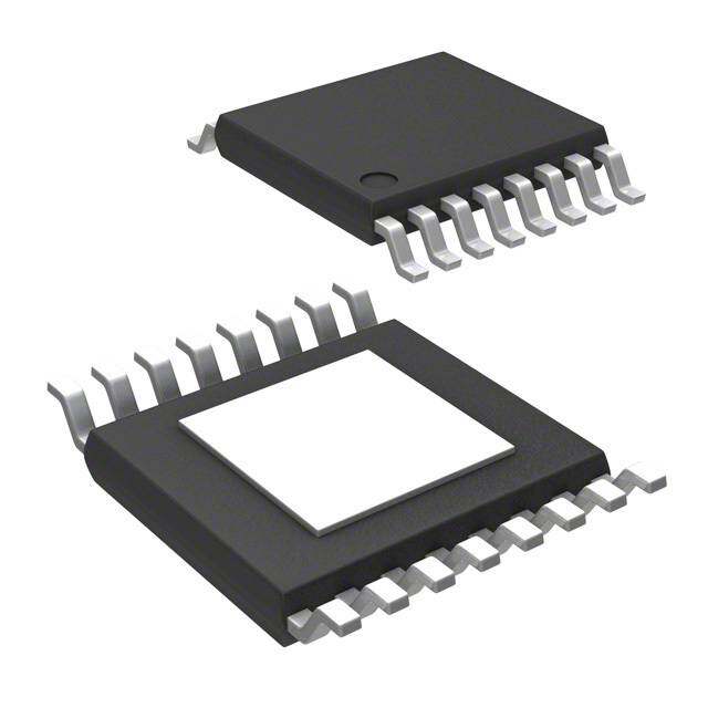
ICGOO电子元器件商城为您提供L6225PDTR由STMicroelectronics设计生产,在icgoo商城现货销售,并且可以通过原厂、代理商等渠道进行代购。 L6225PDTR价格参考。STMicroelectronicsL6225PDTR封装/规格:PMIC - 电机驱动器,控制器, Bipolar Motor Driver BiCDMOS Parallel PowerSO-20。您可以下载L6225PDTR参考资料、Datasheet数据手册功能说明书,资料中有L6225PDTR 详细功能的应用电路图电压和使用方法及教程。
STMicroelectronics(意法半导体)的L6225PDTR是一款用于电机驱动与控制的专用集成电路,属于PMIC中的电机驱动器/控制器类别。该芯片主要用于驱动双极步进电机或直流有刷电机,广泛应用于需要高精度位置控制和运动管理的场合。

典型应用场景包括工业自动化设备中的伺服控制系统、打印机、扫描仪、复印机等办公自动化设备,以及安防摄像头的云台控制、小型机器人关节驱动和医疗设备中的精密移动部件控制。L6225PDTR支持全桥PWM电流控制模式,具备可调节的电流控制功能,能够实现平稳、低噪声的电机运行,并集成过热、过流和欠压保护机制,提升系统可靠性。

其采用PowerSO-36封装,适合紧凑型设计,适用于对空间要求较高的嵌入式系统。此外,该器件具有良好的抗干扰能力和稳定性,可在较宽温度范围内稳定工作,因此也适用于工业级环境。总体而言,L6225PDTR是一款高性能、高集成度的电机驱动解决方案,适用于中低功率、高精度控制需求的应用场景。
| 参数 | 数值 |
| 产品目录 | 集成电路 (IC) |
| 描述 | IC MOTOR DRIVER PAR 20POWERSO |
| 产品分类 | PMIC - 电机, 电桥式驱动器 |
| 品牌 | STMicroelectronics |
| 数据手册 | |
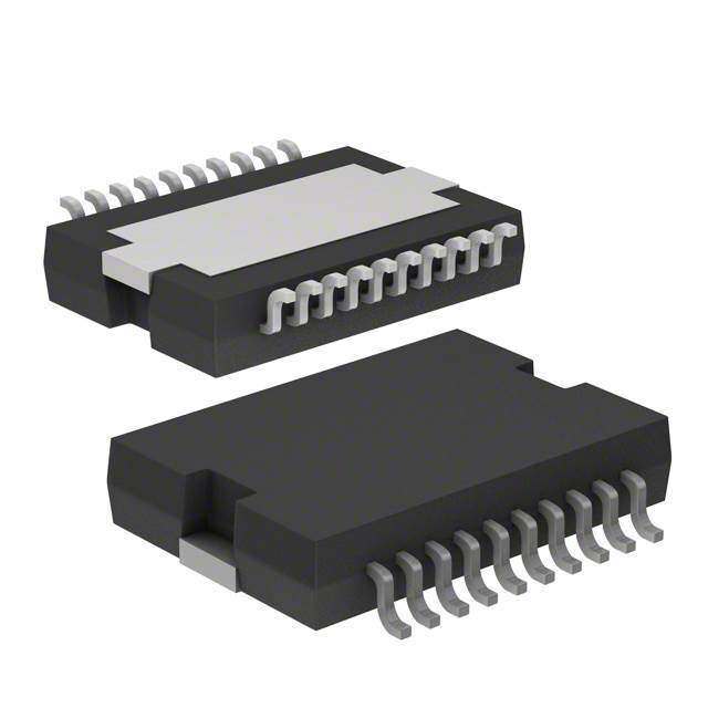
| 产品图片 |
|
| 产品型号 | L6225PDTR |
| rohs | 无铅 / 符合限制有害物质指令(RoHS)规范要求 |
| 产品系列 | - |
| 产品培训模块 | http://www.digikey.cn/PTM/IndividualPTM.page?site=cn&lang=zhs&ptm=9991 |
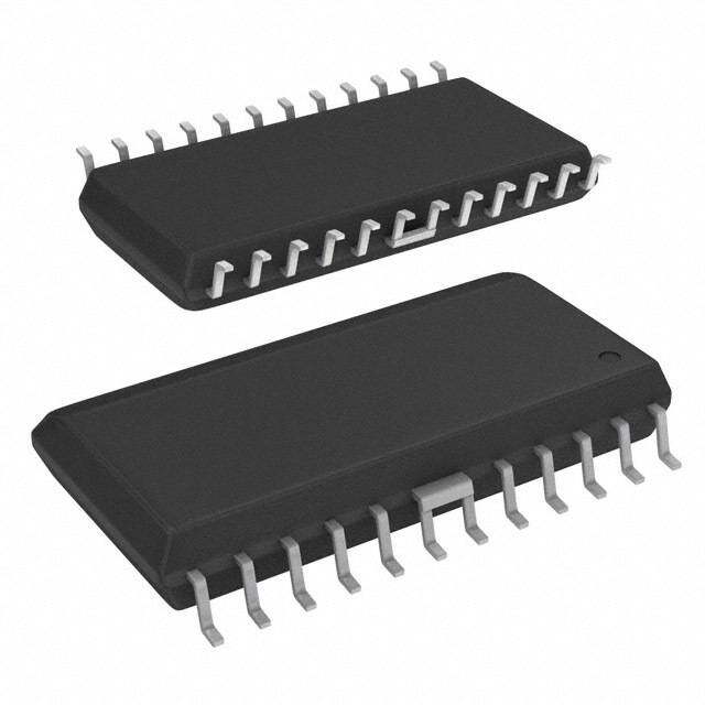
| 供应商器件封装 | PowerSO-20 |
| 其它名称 | 497-5345-6 |
| 其它有关文件 | http://www.st.com/web/catalog/sense_power/FM142/CL851/SC1790/SS1555/LN1632/PF73912?referrer=70071840 |
| 功能 | 驱动器 - 全集成,控制和功率级 |
| 包装 | Digi-Reel® |
| 安装类型 | 表面贴装 |
| 封装/外壳 | 20-SOIC(0.433",11.00mm 宽)裸焊盘 |
| 工作温度 | -25°C ~ 125°C |
| 应用 | 通用 |
| 接口 | 并联 |
| 标准包装 | 1 |
| 电压-电源 | 8 V ~ 52 V |
| 电压-负载 | 8 V ~ 52 V |
| 电机类型-AC,DC | 有刷直流 |
| 电机类型-步进 | 双极性 |
| 电流-输出 | 1.4A |
| 输出配置 | 全 H 桥,(1) 单 |


- 商务部:美国ITC正式对集成电路等产品启动337调查
- 曝三星4nm工艺存在良率问题 高通将骁龙8 Gen1或转产台积电
- 太阳诱电将投资9.5亿元在常州建新厂生产MLCC 预计2023年完工
- 英特尔发布欧洲新工厂建设计划 深化IDM 2.0 战略
- 台积电先进制程称霸业界 有大客户加持明年业绩稳了
- 达到5530亿美元!SIA预计今年全球半导体销售额将创下新高
- 英特尔拟将自动驾驶子公司Mobileye上市 估值或超500亿美元
- 三星加码芯片和SET,合并消费电子和移动部门,撤换高东真等 CEO
- 三星电子宣布重大人事变动 还合并消费电子和移动部门
- 海关总署:前11个月进口集成电路产品价值2.52万亿元 增长14.8%

PDF Datasheet 数据手册内容提取
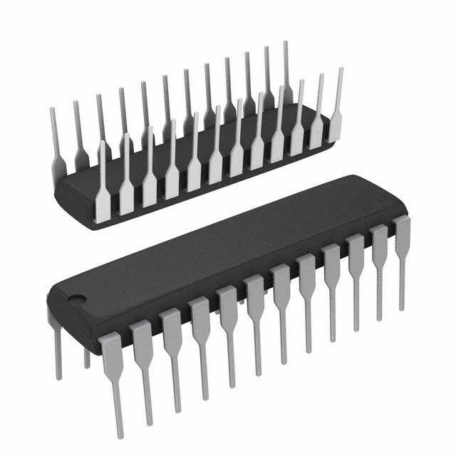
L6225 DMOS DUAL FULL BRIDGE DRIVER n OPERATING SUPPLY VOLTAGE FROM 8 TO 52V n 2.8A OUTPUT PEAK CURRENT (1.4A DC) n RDS(ON) 0.73W TYP. VALUE @ Tj = 25 °C n OPERATING FREQUENCY UP TO 100KHz n NON DISSIPATIVE OVERCURRENT PROTECTION PowerDIP20 PowerSO20 SO20 (16+2+2) (16+2+2) n PARALLELED OPERATION n CROSS CONDUCTION PROTECTION ORDERING NUMBERS: n THERMAL SHUTDOWN L6225N (PowerDIP20) n UNDER VOLTAGE LOCKOUT L6225PD (PowerSO20) n INTEGRATED FAST FREE WHEELING DIODES L6225D (SO20) TYPICAL APPLICATIONS n BIPOLAR STEPPER MOTOR BCD technology, which combines isolated DMOS n DUAL OR QUAD DC MOTOR Power Transistors with CMOS and bipolar circuits on the same chip. Available in PowerDIP20 (16+2+2), DESCRIPTION PowerSO20 and SO20(16+2+2) packages, the The L6225 is a DMOS Dual Full Bridge designed for L6225 features a non-dissipative protection of the motor control applications, realized in MultiPower- high side PowerMOSFETs and thermal shutdown. BLOCK DIAGRAM VBOOT VBOOT VBOOT VBOOT VSA VCP CHARGE PUMP OVER OCDA CURRENT DETECTION OUT1A OUT2A THERMAL 10V 10V PROTECTION ENA GATE LOGIC IN1A SENSEA IN2A VOLTAGE 10V REGULATOR 5V BRIDGE A OVER CURRENT OCDB DETECTION VSB OUT1B GATE OUT2B ENB LOGIC SENSEB IN1B IN2B BRIDGE B D99IN1091A September 2003 1/20
L6225 ABSOLUTE MAXIMUM RATINGS Symbol Parameter Test conditions Value Unit VS Supply Voltage VSA = VSB = VS 60 V VOD Differential Voltage between VSA = VSB = VS = 60V; 60 V VSA, OUT1A, OUT2A, SENSEA and VSENSEA = VSENSEB = GND VSB, OUT1B, OUT2B, SENSEB VBOOT Bootstrap Peak Voltage VSA = VSB = VS VS + 10 V VIN,VEN Input and Enable Voltage Range -0.3 to +7 V VSENSEA, Voltage Range at pins SENSEA -1 to +4 V VSENSEB and SENSEB IS(peak) Pulsed Supply Current (for each VSA = VSB = VS; 3.55 A VS pin), internally limited by the tPULSE < 1ms overcurrent protection IS RMS Supply Current (for each VSA = VSB = VS 1.4 A VS pin) Tstg, TOP Storage and Operating -40 to 150 (cid:176) C Temperature Range RECOMMENDED OPERATING CONDITIONS Symbol Parameter Test Conditions MIN MAX Unit VS Supply Voltage VSA = VSB = VS 8 52 V VOD Differential Voltage Between VSA = VSB = VS; 52 V VSA, OUT1A, OUT2A, SENSEA and VSENSEA = VSENSEB VSB, OUT1B, OUT2B, SENSEB VSENSEA, Voltage Range at pins SENSEA (pulsed tW < trr) -6 6 V VSENSEB and SENSEB (DC) -1 1 V IOUT RMS Output Current 1.4 A Tj Operating Junction Temperature -25 +125 °C fsw Switching Frequency 100 KHz 2/20
L6225 THERMAL DATA Symbol Description PowerDIP20 SO20 PowerSO20 Unit Rth-j-pins MaximumThermal Resistance Junction-Pins 13 15 - (cid:176) C/W Rth-j-case Maximum Thermal Resistance Junction-Case - - 2 (cid:176) C/W Rth-j-amb1 MaximumThermal Resistance Junction-Ambient 1 41 52 - (cid:176) C/W Rth-j-amb1 Maximum Thermal Resistance Junction-Ambient 2 - - 36 (cid:176) C/W Rth-j-amb1 MaximumThermal Resistance Junction-Ambient 3 - - 16 (cid:176) C/W Rth-j-amb2 Maximum Thermal Resistance Junction-Ambient 4 57 78 63 (cid:176) C/W (1) Mounted on a multi-layer FR4 PCB with a dissipating copper surface on the bottom side of 6cm2 (with a thickness of 35µm). (2) Mounted on a multi-layer FR4 PCB with a dissipating copper surface on the top side of 6cm2 (with a thickness of 35µm). (3) Mounted on a multi-layer FR4 PCB with a dissipating copper surface on the top side of 6cm2 (with a thickness of 35µm), 16 via holes and a ground layer. (4) Mounted on a multi-layer FR4 PCB without any heat sinking surface on the board. PIN CONNECTIONS (Top View) IN1 1 20 EN A A GND 1 20 GND IN2 2 19 VCP A VSA 2 19 VSB SENSEA 3 18 OUT2A OUT2A 3 18 OUT2B OUT1A 4 17 VSA VCP 4 17 VBOOT GND 5 16 GND ENA 5 16 ENB GND 6 15 GND IN1A 6 15 IN2B OUT1B 7 14 VSB IN2A 7 14 IN1B SENSEB 8 13 OUT2B SENSEA 8 13 SENSEB IN1B 9 12 VBOOT OUT1A 9 12 OUT1B IN2 10 11 EN GND 10 11 GND B B D99IN1093A D99IN1092A PowerDIP20/SO20 PowerSO20 (5) (5) The slug is internally connected to pins 1,10,11 and 20 (GND pins). 3/20
L6225 PIN DESCRIPTION PACKAGE SO20/ PowerSO20 Name Type Function PowerDIP20 PIN # PIN # 1 6 IN1A Logic Input Bridge A Logic Input 1. 2 7 IN2A Logic Input Bridge A Logic Input 2. 3 8 SENSEA Power Supply Bridge A Source Pin. This pin must be connected to Power Ground directly or through a sensing power resistor. 4 9 OUT1A Power Output Bridge A Output 1. 5, 6, 15, 16 1, 10, 11, GND GND Signal Ground terminals. In PowerDIP and SO packages, 20 these pins are also used for heat dissipation toward the PCB. 7 12 OUT1B Power Output Bridge B Output 1. 8 13 SENSEB Power Supply Bridge B Source Pin. This pin must be connected to Power Ground directly or through a sensing power resistor. 9 14 IN1B Logic Input Bridge B Logic Input 1. 10 15 IN2B Logic Input Bridge B Logic Input 2. 11 16 ENB Logic Input (6) Bridge B Enable. LOW logic level switches OFF all Power MOSFETs of Bridge B. This pin is also connected to the collector of the Overcurrent and Thermal Protection transistor to implement over current protection. If not used, it has to be connected to +5V through a resistor. 12 17 VBOOT Supply Bootstrap Voltage needed for driving the upper Voltage PowerMOSFETs of both Bridge A and Bridge B. 13 18 OUT2B Power Output Bridge B Output 2. 14 19 VSB Power Supply Bridge B Power Supply Voltage. It must be connected to the supply voltage together with pin VSA. 17 2 VSA Power Supply Bridge A Power Supply Voltage. It must be connected to the supply voltage together with pin VSB. 18 3 OUT2A Power Output Bridge A Output 2. 19 4 VCP Output Charge Pump Oscillator Output. 20 5 ENA Logic Input (6) Bridge A Enable. LOW logic level switches OFF all Power MOSFETs of Bridge A. This pin is also connected to the collector of the Overcurrent and Thermal Protection transistor to implement over current protection. If not used, it has to be connected to +5V through a resistor. (6) Also connected at the output drain of the Overcurrent and Thermal protection MOSFET. Therefore, it has to be driven putting in series a resistor with a value in the range of 2.2kW - 180KW , recommended 100kW 4/20
L6225 ELECTRICAL CHARACTERISTICS (Tamb = 25 °C, Vs = 48V, unless otherwise specified) Symbol Parameter Test Conditions Min Typ Max Unit VSth(ON) Turn-on Threshold 5.8 6.3 6.8 V VSth(OFF) Turn-off Threshold 5 5.5 6 V IS Quiescent Supply Current All Bridges OFF; 5 10 mA Tj = -25°C to 125°C (7) Tj(OFF) Thermal Shutdown Temperature 165 (cid:176) C Output DMOS Transistors RDS(ON) High-Side + Low-Side Switch ON Tj = 25 (cid:176) C 1.47 1.69 W Resistance Tj =125 (cid:176) C (7) 2.35 2.70 W IDSS Leakage Current EN = Low; OUT = VS 2 mA EN = Low; OUT = GND -0.3 mA Source Drain Diodes VSD Forward ON Voltage ISD = 1.4A, EN = LOW 1.15 1.3 V trr Reverse Recovery Time If = 1.4A 300 ns tfr Forward Recovery Time 200 ns Logic Input VIL Low level logic input voltage -0.3 0.8 V VIH High level logic input voltage 2 7 V IIL Low Level Logic Input Current GND Logic Input Voltage -10 µA IIH High Level Logic Input Current 7V Logic Input Voltage 10 µA Vth(ON) Turn-on Input Threshold 1.8 2.0 V Vth(OFF) Turn-off Input Threshold 0.8 1.3 V Vth(HYS) Input Threshold Hysteresis 0.25 0.5 V Switching Characteristics tD(on)EN Enable to out turn ON delay time (8) ILOAD =1.4A, Resistive Load 500 800 ns tD(on)IN Input to out turn ON delay time ILOAD =1.4A, Resistive Load 1.9 µs (dead time included) tRISE Output rise time(8) ILOAD =1.4A, Resistive Load 40 250 ns tD(off)EN Enable to out turn OFF delay time (8) ILOAD =1.4A, Resistive Load 500 800 1000 ns tD(off)IN Input to out turn OFF delay time ILOAD =1.4A, Resistive Load 500 800 1000 ns tFALL Output Fall Time (8) ILOAD =1.4A, Resistive Load 40 250 ns 5/20
L6225 ELECTRICAL CHARACTERISTICS (continued) (Tamb = 25 °C, Vs = 48V, unless otherwise specified) Symbol Parameter Test Conditions Min Typ Max Unit tdt Dead Time Protection 0.5 1 µs fCP Charge pump frequency -25°C<Tj <125°C 0.6 1 MHz Over Current Protection ISOVER Input Supply Overcurrent Tj = -25°C to 125°C (7) 2 2.8 3.55 A Protection Threshold ROPDR Open Drain ON Resistance I = 4mA 40 60 W tOCD(ON) OCD Turn-on Delay Time (9) I = 4mA; CEN < 100pF 200 ns tOCD(OFF) OCD Turn-off Delay Time (9) I = 4mA; CEN < 100pF 100 ns (7) Tested at 25°C in a restricted range and guaranteed by characterization. (8) See Fig. 1. (9) See Fig. 2. Figure 1. Switching Characteristic Definition EN Vth(ON) Vth(OFF) t IOUT 90% 10% t D01IN1316 tFALL tRISE tD(OFF)EN tD(ON)EN 6/20
L6225 Figure 2. Overcurrent Detection Timing Definition I OUT I SOVER ON BRIDGE OFF V EN 90% 10% D02IN1399 t t OCD(ON) OCD(OFF) 7/20
L6225 CIRCUIT DESCRIPTION POWER STAGES and CHARGE PUMP The L6225 integrates two independent Power MOS (collector) structure, a pull-up resistor REN and a ca- Full Bridges. Each Power MOS has an Rd- pacitor CEN are connected as shown in Fig. 5. If the son=0.73ohm (typical value @25°C), with intrinsic driver is a standard Push-Pull structure the resistor fast freewheeling diode. Cross conduction protection R and the capacitor C are connected as shown EN EN is achieved using a dead time (td = 1m s typical) be- in Fig. 6. The resistor R should be chosen in the EN tween the switch off and switch on of two Power MOS range from 2.2kW to 180KW . Recommended values in one leg of a bridge. for REN and CEN are respectively 100KW and 5.6nF. Using N Channel Power MOS for the upper transis- More information on selecting the values is found in tors in the bridge requires a gate drive voltage above the Overcurrent Protection section. the power supply voltage. The Bootstrapped (Vboot) supply is obtained through an internal Oscillator and Figure 4. Logic Inputs Internal Structure few external components to realize a charge pump 5V circuit as shown in Figure 3. The oscillator output (VCP) is a square wave at 600kHz (typical) with 10V amplitude. Recommended values/part numbers for the charge pump circuit are shown in Table1. ESD PROTECTION D01IN1329 Table 1. Charge Pump External Components Values Figure 5. ENA and ENB Pins Open Collector CBOOT 220nF Driving CP 10nF 5V RP 100W 5V REN D1 1N4148 D2 1N4148 COLOLPEECNTOR ENA or ENB OUTPUT CEN Figure 3. Charge Pump Circuit D02IN1349 VS D1 CBOOT Figure 6. ENA and ENB Pins Push-Pull Driving D2 5V RP PUSH-PULL REN ENA or ENB CP OUTPUT CEN VCP VBOOT VSA VSB D01IN1328 LOGIC INPUTS D02IN1350 Pins IN1A, IN2A, IN1B and IN2B are TTL/CMOS and m C compatible logic inputs. The internal structure is TRUTH TABLE shown in Fig. 4. Typical value for turn-on and turn-off thresholds are respectively Vthon=1.8V and INPUTS OUTPUTS Vthoff=1.3V. EN IN1 IN2 OUT1 OUT2 Pins ENA and ENB have identical input structure with L X X High Z High Z the exception that the drains of the Overcurrent and H L L GND GND thermal protection MOSFETs (one for the Bridge A H H L Vs GND and one for the Bridge B) are also connected to these H L H GND Vs pins. Due to these connections some care needs to H H H Vs Vs be taken in driving these pins. The ENA and ENB in- puts may be driven in one of two configurations as X = Don't care shown in figures 5 or 6. If driven by an open drain High Z = High Impedance Output 8/20
L6225 NON-DISSIPATIVE OVERCURRENT PROTECTION The L6225 integrates an Overcurrent Detection Circuit (OCD). This circuit provides protection against a short circuit to ground or between two phases of the bridge. With this internal over current detection, the external cur- rent sense resistor normally used and its associated power dissipation are eliminated. Figure 7 shows a simpli- fied schematic of the overcurrent detection circuit. To implement the over current detection, a sensing element that delivers a small but precise fraction of the out- put current is implemented with each high side power MOS. Since this current is a small fraction of the output current there is very little additional power dissipation. This current is compared with an internal reference cur- rent IREF. When the output current in one bridge reaches the detection threshold (typically 2.8A) the relative OCD comparator signals a fault condition. When a fault condition is detected, the EN pin is pulled below the turn off threshold (1.3V typical) by an internal open drain MOS with a pull down capability of 4mA. By using an ex- ternal R-C on the EN pin, the off time before recovering normal operation can be easily programmed by means of the accurate thresholds of the logic inputs. Figure 7. Overcurrent Protection Simplified Schematic OUT1A VSA OUT2A POWER SENSE HIGH SIDE DMOSs OF 1 cell THE BRIDGE A I1A I2A POWER SENSE POWER DMOS POWER DMOS 1 cell TO GATE n cells n cells LOGIC + mC or LOGIC OCD I1A / n I2A / n COMPARATOR +5V (I1A+I2A) / n REN ENA INTERNAL IREF OPEN-DRAIN CEN RDS(ON) 40W TYP. OVER TEMPERATURE D02IN1353 Figure 8 shows the Overcurrent Detection operation. The Disable Time tDISABLE before recovering normal opera- tion can be easily programmed by means of the accurate thresholds of the logic inputs. It is affected whether by C and R values and its magnitude is reported in Figure 9. The Delay Time t before turning off the bridge EN EN DELAY when an overcurrent has been detected depends only by CEN value. Its magnitude is reported in Figure 10. CEN is also used for providing immunity to pin EN against fast transient noises. Therefore the value of CEN should be chosen as big as possible according to the maximum tolerable Delay Time and the REN value should be chosen according to the desired Disable Time. The resistor R should be chosen in the range from 2.2KW to 180KW . Recommended values for R and C EN EN EN are respectively 100KW and 5.6nF that allow obtaining 200m s Disable Time. 9/20
L6225 Figure 8. Overcurrent Protection Waveforms I OUT I SOVER V EN V DD V th(ON) V th(OFF) V EN(LOW) ON OCD OFF ON BRIDGE tDELAY tDISABLE OFF t t t t t OCD(ON) EN(FALL) OCD(OFF) EN(RISE) D(ON)EN t D(OFF)EN D02IN1400 10/20
L6225 Figure 9. tDISABLE versus CEN and REN (VDD = 5V). RR == 222200 kkWW RR == 110000 kkWW 11..110033 EENN EENN RREENN == 4477 kkWW RR == 3333 kkWW EENN RR == 1100 kkWW EENN ]] 110000 ss µµ [[ EE LL BB AA SS DIDI tt 1100 11 11 1100 110000 CC [[nnFF]] EENN Figure 10. tDELAY versus CEN (VDD = 5V). 10 s] may [ 1 el d t 0.1 1 10 100 Cen [nF] THERMAL PROTECTION In addition to the Ovecurrent Protection, the L6225 integrates a Thermal Protection for preventing the device destruction in case of junction over temperature. It works sensing the die temperature by means of a sensible element integrated in the die. The device switch-off when the junction temperature reaches 165°C (typ. value) with 15°C hysteresis (typ. value). 11/20
L6225 APPLICATION INFORMATION A typical application using L6225 is shown in Fig. 11. Typical component values for the application are shown in Table 2. A high quality ceramic capacitor in the range of 100 to 200 nF should be placed between the power pins (VSA and VSB) and ground near the L6225 to improve the high frequency filtering on the power supply and reduce high frequency transients generated by the switching. The capacitors connected from the EN and EN A B inputs to ground set the shut down time for the Brgidge A and Bridge B respectively when an over current is detected (see Overcurrent Protection). The two current sources (SENSE and SENSE ) should be connected A B to Power Ground with a trace length as short as possible in the layout. To increase noise immunity, unused logic pins (except ENA and ENB) are best connected to 5V (High Logic Level) or GND (Low Logic Level) (see pin description). It is recommended to keep Power Ground and Signal Ground separated on PCB. Table 2. Component Values for Typical Application C1 100uF D1 1N4148 C2 100nF D2 1N4148 CBOOT 220nF RENA 100KW CP 10nF RENB 100KW CENA 5.6nF RP 100W CENB 5.6nF Figure 11. Typical Application VS + A 17 ENA RENA VS VSB 20 ENABLEA C C 14 8-52VDC 1 2 CENA POWER GROUND D - 1 RP VCP ENB RENB 19 11 ENABLE B C C CBOOT D2 P ENB SIGNAL VBOOT 12 GROUND IN1 B SENSEA 3 9 IN1B IN2 B SENSEB 8 10 IN2B IN1 A 1 IN1 LOADA OUT1A A 4 IN2 A OUT2 2 IN2 A A 18 16 LOADB OUT1B GND 7 15 OUT2 GND B 13 6 GND 5 GND D02IN1345 12/20
L6225 PARALLELED OPERATION The outputs of the L6225 can be paralleled to increase the output current capability or reduce the power dissi- pation in the device at a given current level. It must be noted, however, that the internal wire bond connections from the die to the power or sense pins of the package must carry current in both of the associated half bridges. When the two halves of one full bridge (for example OUT1A and OUT2A) are connected in parallel, the peak current rating is not increased since the total current must still flow through one bond wire on the power supply or sense pin. In addition, the over current detection senses the sum of the current in the upper devices of each bridge (A or B) so connecting the two halves of one bridge in parallel does not increase the over current detec- tion threshold. For most applications the recommended configuration is Half Bridge 1 of Bridge A paralleled with the Half Bridge 1 of the Bridge B, and the same for the Half Bridges 2 as shown in Figure 12. The current in the two devices connected in parallel will share very well since the RDS(ON) of the devices on the same die is well matched. In this configuration the resulting Bridge has the following characteristics. - Equivalent Device: FULL BRIDGE - R 0.37W Typ. Value @ T = 25°C DS(ON) J - 2.8A max RMS Load Current - 5.6A OCD Threshold Figure 12. Parallel connection for higher current VS A + 17 VS C C VSB 14 11 ENB 8-52V 1 2 PDCOWER 20 ENA REN EN GROUND D - 1 RP VCP CEN 19 C CBOOT D2 P SIGNAL VBOOT IN1A GROUND 12 1 IN1 SENSEA 3 2 IN2A SENSEB 8 9 IN1B OUT1 IN2 A B 4 10 IN2 OUT2 GND A 18 16 GND LOAD OUT1 15 B 7 GND 6 OUT2 GND B 13 5 D02IN1359 To operate the device in parallel and maintain a lower over current threshold, Half Bridge 1 and the Half Bridge 2 of the Bridge A can be connected in parallel and the same done for the Bridge B as shown in Figure 13. In this configuration, the peak current for each half bridge is still limited by the bond wires for the supply and sense pins so the dissipation in the device will be reduced, but the peak current rating is not increased. This configu- ration, the resulting bridge has the following characteristics. - Equivalent Device: FULL BRIDGE - RDS(ON) 0.37W Typ. Value @ TJ = 25°C - 1.4A max RMS Load Current - 2.8A OCD Threshold 13/20
L6225 Figure 13. Parallel connection with lower Overcurrent Threshold VS + A 17 8-5V2SVDC C1 C2 VSB 14 20 ENA POWER G-ROUND D1 RP VCP 11 ENB REN EN 19 C C EN CBOOT D2 P SIGNAL VBOOT GROUND 12 1 IN1A SENSE A 3 IN2 2 A IN A SENSE B 8 IN1 9 B IN OUT1 B A 4 IN2 10 B OUT2 A 18 GND 16 LOAD OUT1 GND B 7 15 GND OUT2 6 B 13 GND 5 D02IN1360 It is also possible to parallel the four Half Bridges to obtain a simple Half Bridge as shown in Fig. 14 The resulting half bridge has the following characteristics. - Equivalent Device: HALF BRIDGE - R 0.18W Typ. Value @ T = 25°C DS(ON) J - 2.8A max RMS Load Current - 5.6A OCD Threshold Figure 14. Paralleling the four Half Bridges VS A + 17 VS C C VSB 14 11 ENB 8-52V 1 2 PDCOWER 20 ENA REN EN GROUND D - 1 RP VCP CEN 19 C CBOOT D2 P IN1A SIGNAL VBOOT 1 12 GROUND IN2 A SENSE 2 A 3 IN SENSEB 8 9 IN1B OUT1 IN2 A B 4 10 OUT2 GND A 18 16 LOAD GND 15 OUT1 GND B 7 6 GND OUT2 5 B 13 D02IN1366 14/20
L6225 OUTPUT CURRENT CAPABILITY AND IC POWER DISSIPATION In Fig. 15 and Fig. 16 are shown the approximate relation between the output current and the IC power dissipa- tion using PWM current control driving two loads, for two different driving types: – One Full Bridge ON at a time (Fig. 15) in which only one load at a time is energized. – Two Full Bridges ON at the same time (Fig. 16) in which two loads at the same time are energized. For a given output current and driving type the power dissipated by the IC can be easily evaluated, in order to establish which package should be used and how large must be the on-board copper dissipating area to guar- antee a safe operating junction temperature (125°C maximum). Figure 15. IC Power Dissipation versus Output Current with One Full Bridge ON at a time. ONE FULL BRIDGE ON AT A TIME 10 I A I OUT 8 I B 6 P [W] I D OUT 4 Test Conditions: 2 Supply Voltage = 24V No PWM 0 0 0.25 0.5 0.75 1 1.25 1.5 f = 30 kHz (slow decay) SW I [A] OUT Figure 16. IC Power Dissipation versus Output Current with Two Full Bridges ON at the same time. TWO FULL BRIDGES ON AT THE SAME TIME I 10 A I OUT 8 I B 6 PD [W] IOUT 4 Test Conditions: 2 Supply Voltage = 24 V 0 No PWM 0 0.25 0.5 0.75 1 1.25 1.5 f = 30 kHz (slow decay) I [A] SW OUT THERMAL MANAGEMENT In most applications the power dissipation in the IC is the main factor that sets the maximum current that can be de- liver by the device in a safe operating condition. Therefore, it has to be taken into account very carefully. Besides the available space on the PCB, the right package should be chosen considering the power dissipation. Heat sinking can be achieved using copper on the PCB with proper area and thickness. Figures 18, 19 and 20 show the Junction-to- Ambient Thermal Resistance values for the PowerSO20, PowerDIP20 and SO20 packages. For instance, using a PowerSO package with copper slug soldered on a 1.5 mm copper thickness FR4 board with 6cm2 dissipating footprint (copper thickness of 35µm), the Rth j-amb is about 35°C/W. Fig. 17 shows mount- ing methods for this package. Using a multi-layer board with vias to a ground plane, thermal impedance can be reduced down to 15°C/W. 15/20
L6225 Figure 17. Mounting the PowerSO package. Slug soldered Slug soldered Slug soldered to PCB with to PCB with to PCB with dissipating area plus ground layer dissipating area dissipating area contacted through via holes plus ground layer Figure 18. PowerSO20 Junction-Ambient thermal resistance versus on-board copper area. ºC / W 43 38 33 Without Ground Layer 28 With Ground Layer With Ground Layer+16 via 23 Holes On-Board Copper Area 18 13 1 2 3 4 5 6 7 8 9 10 11 12 13 sq. cm Figure 19. PowerDIP20 Junction-Ambient thermal resistance versus on-board copper area. ºC /W On-Board Copper Area 42 41 Copper Area is on Bottom Side 40 39 Copper Area is on Top Side 38 37 36 35 34 33 1 2 3 4 5 6 7 8 9 10 11 12 sq. cm Figure 20. SO20 Junction-Ambient thermal resistance versus on-board copper area. ºC / W On-Board Copper Area 68 66 64 62 60 Copper Area is on Top Side 58 56 54 52 50 48 1 2 3 4 5 6 7 8 9 10 11 12 sq. cm 16/20
L6225 mm inch DIM. MIN. TYP. MAX. MIN. TYP. MAX. OUTLINE AND A 3.6 0.142 MECHANICAL DATA a1 0.1 0.3 0.004 0.012 a2 3.3 0.130 a3 0 0.1 0.000 0.004 b 0.4 0.53 0.016 0.021 Weight:1.9gr c 0.23 0.32 0.009 0.013 D (1) 15.8 16 0.622 0.630 D1 9.4 9.8 0.370 0.386 E 13.9 14.5 0.547 0.570 e 1.27 0.050 e3 11.43 0.450 E1 (1) 10.9 11.1 0.429 0.437 E2 2.9 0.114 E3 5.8 6.2 0.228 0.244 G 0 0.1 0.000 0.004 H 15.5 15.9 0.610 0.626 h 1.1 0.043 JEDEC MO-166 L 0.8 1.1 0.031 0.043 N 8˚ (typ.) S 8˚ (max.) T 10 0.394 PowerSO20 (1) “D and E1” do not include mold flash or protusions. - Mold flash or protusions shall not exceed 0.15mm (0.006”) - Critical dimensions: “E”, “G” and “a3”. N N R a2 A c a1 b e DETAIL B DETAIL A E e3 H lead DETAIL A D slug a3 DETAIL B 20 11 0.35 Gage Plane - C - S L SEATING PLANE G C E2 E1 BOTTOM VIEW (COPLANARITY) T E3 1 10 D1 h x 45 PSO20MEC 0056635 17/20
L6225 mm inch OUTLINE AND DIM. MECHANICAL DATA MIN. TYP. MAX. MIN. TYP. MAX. a1 0.51 0.020 B 0.85 1.40 0.033 0.055 b 0.50 0.020 b1 0.38 0.50 0.015 0.020 D 24.80 0.976 E 8.80 0.346 e 2.54 0.100 e3 22.86 0.900 F 7.10 0.280 I 5.10 0.201 L 3.30 0.130 Powerdip 20 Z 1.27 0.050 18/20
L6225 mm inch OUTLINE AND DIM. MECHANICAL DATA MIN. TYP. MAX. MIN. TYP. MAX. A 2.35 2.65 0.093 0.104 A1 0.1 0.3 0.004 0.012 B 0.33 0.51 0.013 0.020 C 0.23 0.32 0.009 0.013 D 12.6 13 0.496 0.512 E 7.4 7.6 0.291 0.299 e 1.27 0.050 H 10 10.65 0.394 0.419 h 0.25 0.75 0.010 0.030 L 0.4 1.27 0.016 0.050 SO20 K 0˚ (min.)8˚ (max.) L h x 45˚ A B e K A1 C H D 20 11 E 1 10 SO20MEC 19/20
L6225 Information furnished is believed to be accurate and reliable. However, STMicroelectronics assumes no responsibility for the consequences of use of such information nor for any infringement of patents or other rights of third parties which may result from its use. No license is granted by implication or otherwise under any patent or patent rights of STMicroelectronics. Specifications mentioned in this publication are subject to change without notice. This publication supersedes and replaces all information previously supplied. STMicroelectronics products are not authorized for use as critical components in life support devices or systems without express written approval of STMicroelectronics. The ST logo is a registered trademark of STMicroelectronics. All other names are the property of their respective owners © 2003 STMicroelectronics - All rights reserved STMicroelectronics GROUP OF COMPANIES Australia - Belgium - Brazil - Canada - China - Czech Republic - Finland - France - Germany - Hong Kong - India - Israel - Italy - Japan - Malaysia - Malta - Morocco - Singapore - Spain - Sweden - Switzerland - United Kingdom - United States www.st.com 20/20