ICGOO在线商城 > L5962
 Datasheet下载
- 型号: L5962
- 制造商: STMicroelectronics
- 库位|库存: xxxx|xxxx
- 要求:
| 数量阶梯 | 香港交货 | 国内含税 |
| +xxxx | $xxxx | ¥xxxx |
查看当月历史价格
查看今年历史价格
L5962产品简介:
ICGOO电子元器件商城为您提供L5962由STMicroelectronics设计生产,在icgoo商城现货销售,并且可以通过原厂、代理商等渠道进行代购。 提供L5962价格参考以及STMicroelectronicsL5962封装/规格参数等产品信息。 你可以下载L5962参考资料、Datasheet数据手册功能说明书, 资料中有L5962详细功能的应用电路图电压和使用方法及教程。
| 参数 | 数值 |
| 产品目录 | 集成电路 (IC)半导体 |
| 描述 | IC VREG MULTIFUNCTION POWERSO36低压差稳压器 Multifunction Voltage Regulator |
| 产品分类 | |
| 品牌 | STMicroelectronics |
| 产品手册 | |
| 产品图片 | |
| rohs | 符合RoHS无铅 / 符合限制有害物质指令(RoHS)规范要求 |
| 产品系列 | 电源管理 IC,低压差稳压器,STMicroelectronics L5962- |
| 数据手册 | |
| 产品型号 | L5962 |
| 产品种类 | 低压差稳压器 |
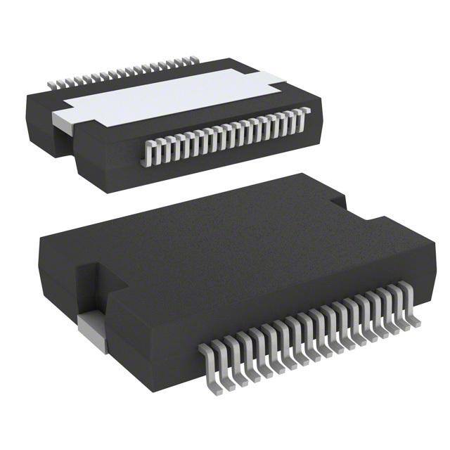
| 供应商器件封装 | PowerSO-36 |
| 其它名称 | 497-11738-5 |
| 其它有关文件 | http://www.st.com/web/catalog/sense_power/FM1965/SC1220/PF250060?referrer=70071840 |
| 包装 | 管件 |
| 商标 | STMicroelectronics |
| 回动电压—最大值 | 600 mV |
| 安装类型 | 表面贴装 |
| 安装风格 | SMD/SMT |
| 封装 | Tube |
| 封装/外壳 | PowerSO-36 裸露顶部焊盘 |
| 封装/箱体 | PowerSO-36 |
| 工作温度 | -40°C ~ 85°C |
| 工厂包装数量 | 31 |
| 应用 | 转换器,汽车音响系统 |
| 最大工作温度 | + 85 C |
| 最大输入电压 | 50 V |
| 最小工作温度 | - 40 C |
| 标准包装 | 31 |
| 电压-输入 | 4.1 V ~ 27 V |
| 电压-输出 | 多重 |
| 系列 | L5962 |
| 线路调整率 | 50 mV |
| 负载调节 | 20 mV |
| 输出数 | 5 |
| 输出电压 | 1.2 V to 8 V |
| 输出电流 | 150 mA |
| 输出类型 | Selectable |


- 商务部:美国ITC正式对集成电路等产品启动337调查
- 曝三星4nm工艺存在良率问题 高通将骁龙8 Gen1或转产台积电
- 太阳诱电将投资9.5亿元在常州建新厂生产MLCC 预计2023年完工
- 英特尔发布欧洲新工厂建设计划 深化IDM 2.0 战略
- 台积电先进制程称霸业界 有大客户加持明年业绩稳了
- 达到5530亿美元!SIA预计今年全球半导体销售额将创下新高
- 英特尔拟将自动驾驶子公司Mobileye上市 估值或超500亿美元
- 三星加码芯片和SET,合并消费电子和移动部门,撤换高东真等 CEO
- 三星电子宣布重大人事变动 还合并消费电子和移动部门
- 海关总署:前11个月进口集成电路产品价值2.52万亿元 增长14.8%


PDF Datasheet 数据手册内容提取
L5962 Multiple linear/switching voltage regulator for car-radio Features ■ Step-down synchronous switching voltage regulator – Internal high-side/ Low-side NDMOS – 1.2 < V < 8 V selectable through external out resistors – 1.2/2.5 A load current selected through PowerSO36 (slug-up) dedicated pin – 185 kHz free-run frequency ■ Enable pin to drive switching regulator and I2C – SYNC function (220 < f < 400 kHz) sw bus logic ■ Linear regulators ■ Under/over voltage battery detector – 3.3/5 V @ 150 mA standby regulator (VBATVW) selected through dedicated pin – Under voltage threshold adjustable through (VSTBYSEL) dedicated pin (LVWIN) – 5/8.5 V @ 350 mA switched linear regulator enabled and selected through I2C bus ■ Load dump protection (VLR1) ■ Independent thermal protection on all – 3.3/10 V @ 1 A switched linear regulator regulators enabled and selected through I2C bus (VLR2) Description ■ 2 High side drivers (0.5 V max drop @ 0.5 A) enabled through I2C bus and equipped with L5962 is a very versatile device exploiting BCD technology characteristics to provide a complete protection circuit against: set of regulated voltages covering all the needs of – short to ground and battery a car-radio set. – loss of ground and battery In standby condition the device guarantees – unsupplied short to battery extremely low quiescent current (90 µA max - ■ Reset function with configurable delay (RST, 40°C < T < 85 °C) and minimum operating RSTDLY) voltage (4.5 V using an external Schottky diode ■ I2C bus for the back-up function). T able 1. Device summary Order code Package Packing L5962 PowerSO36 Tray L5962TR PowerSO36 Tape and reel September 2013 Doc ID 16819 Rev 3 1/24 www.st.com 1
Contents L5962 Contents 1 Block and application diagram . . . . . . . . . . . . . . . . . . . . . . . . . . . . . . . . 5 2 Pin description . . . . . . . . . . . . . . . . . . . . . . . . . . . . . . . . . . . . . . . . . . . . . 7 3 Electrical specification . . . . . . . . . . . . . . . . . . . . . . . . . . . . . . . . . . . . . . . 9 3.1 Absolute maximum ratings . . . . . . . . . . . . . . . . . . . . . . . . . . . . . . . . . . . . . 9 3.2 Thermal data . . . . . . . . . . . . . . . . . . . . . . . . . . . . . . . . . . . . . . . . . . . . . . . 9 3.3 Electrical characteristics . . . . . . . . . . . . . . . . . . . . . . . . . . . . . . . . . . . . . . . 9 4 Device description . . . . . . . . . . . . . . . . . . . . . . . . . . . . . . . . . . . . . . . . . 15 4.1 Regulators . . . . . . . . . . . . . . . . . . . . . . . . . . . . . . . . . . . . . . . . . . . . . . . . 15 4.1.1 Linear regulators . . . . . . . . . . . . . . . . . . . . . . . . . . . . . . . . . . . . . . . . . . 15 4.1.2 Switching regulator . . . . . . . . . . . . . . . . . . . . . . . . . . . . . . . . . . . . . . . . 16 4.2 High side drivers . . . . . . . . . . . . . . . . . . . . . . . . . . . . . . . . . . . . . . . . . . . . 17 5 Operating mode . . . . . . . . . . . . . . . . . . . . . . . . . . . . . . . . . . . . . . . . . . . . 18 5.1 Battery detection . . . . . . . . . . . . . . . . . . . . . . . . . . . . . . . . . . . . . . . . . . . 18 6 I2C bus interface . . . . . . . . . . . . . . . . . . . . . . . . . . . . . . . . . . . . . . . . . . . 19 6.1 Data validity . . . . . . . . . . . . . . . . . . . . . . . . . . . . . . . . . . . . . . . . . . . . . . . 19 6.2 Start and stop conditions . . . . . . . . . . . . . . . . . . . . . . . . . . . . . . . . . . . . . 19 6.3 Byte format . . . . . . . . . . . . . . . . . . . . . . . . . . . . . . . . . . . . . . . . . . . . . . . . 19 6.4 Acknowledge . . . . . . . . . . . . . . . . . . . . . . . . . . . . . . . . . . . . . . . . . . . . . . 19 7 Software specifications . . . . . . . . . . . . . . . . . . . . . . . . . . . . . . . . . . . . . 21 8 Package information . . . . . . . . . . . . . . . . . . . . . . . . . . . . . . . . . . . . . . . . 22 9 Revision history . . . . . . . . . . . . . . . . . . . . . . . . . . . . . . . . . . . . . . . . . . . 23 2/24 Doc ID 16819 Rev 3
L5962 List of tables List of tables Table 1. Device summary. . . . . . . . . . . . . . . . . . . . . . . . . . . . . . . . . . . . . . . . . . . . . . . . . . . . . . . . . . 1 Table 2. Pin description . . . . . . . . . . . . . . . . . . . . . . . . . . . . . . . . . . . . . . . . . . . . . . . . . . . . . . . . . . . 7 Table 3. Absolute maximum ratings. . . . . . . . . . . . . . . . . . . . . . . . . . . . . . . . . . . . . . . . . . . . . . . . . . 9 Table 4. Thermal data. . . . . . . . . . . . . . . . . . . . . . . . . . . . . . . . . . . . . . . . . . . . . . . . . . . . . . . . . . . . . 9 Table 5. Electrical characteristics. . . . . . . . . . . . . . . . . . . . . . . . . . . . . . . . . . . . . . . . . . . . . . . . . . . . 9 Table 6. Chip address. . . . . . . . . . . . . . . . . . . . . . . . . . . . . . . . . . . . . . . . . . . . . . . . . . . . . . . . . . . . 21 Table 7. IB1 data byte. . . . . . . . . . . . . . . . . . . . . . . . . . . . . . . . . . . . . . . . . . . . . . . . . . . . . . . . . . . . 21 Table 8. VLR2 output level selection . . . . . . . . . . . . . . . . . . . . . . . . . . . . . . . . . . . . . . . . . . . . . . . . 21 Table 9. Document revision history . . . . . . . . . . . . . . . . . . . . . . . . . . . . . . . . . . . . . . . . . . . . . . . . . 23 Doc ID 16819 Rev 3 3/24
List of figures L5962 List of figures Figure 1. Block diagram. . . . . . . . . . . . . . . . . . . . . . . . . . . . . . . . . . . . . . . . . . . . . . . . . . . . . . . . . . . . 5 Figure 2. Application diagram . . . . . . . . . . . . . . . . . . . . . . . . . . . . . . . . . . . . . . . . . . . . . . . . . . . . . . . 6 Figure 3. Pin connection (top view) . . . . . . . . . . . . . . . . . . . . . . . . . . . . . . . . . . . . . . . . . . . . . . . . . . . 7 Figure 4. Low voltage warning high level block diagram. . . . . . . . . . . . . . . . . . . . . . . . . . . . . . . . . . 18 Figure 5. Data validity on the I2C bus . . . . . . . . . . . . . . . . . . . . . . . . . . . . . . . . . . . . . . . . . . . . . . . . 19 Figure 6. Timing diagram on the I2C bus. . . . . . . . . . . . . . . . . . . . . . . . . . . . . . . . . . . . . . . . . . . . . . 20 Figure 7. Acknowledge on the I2C bus . . . . . . . . . . . . . . . . . . . . . . . . . . . . . . . . . . . . . . . . . . . . . . . 20 Figure 8. PowerSO36 (slug-up) mechanical data and package dimensions. . . . . . . . . . . . . . . . . . . 22 4/24 Doc ID 16819 Rev 3
L5962 Block and application diagram 1 Block and application diagram Figure 1. Block diagram VINSW VBATP Bandgap Reference PH CBS Switching CLIM External POR & Regulator Storage Startup Logic VFB VCMP SOST VSTBYSEL Standby Regulator VSTBY Oscillator SYNCH Clock LVWIN Linear UV / OV VLR1 Regulator VBATVW Detect Synch #1 Logic RST Reset & Delay Linear RSTDLY VINLR2 Regulator VLR2 #2 SDA SCL I2Cbus Logic HSD HSD1 EN Ground HSD HSD2 AC00428 TABPGNDAGNDSUBS VBAT Doc ID 16819 Rev 3 5/24
Block and application diagram L5962 Figure 2. Application diagram AT 1000u/50V B V T U O VDC 2.2µ HSD1 0.1µ 2 D S H µ 1 V 0. 0 V u/1 25 200 70µ/ 4 H 7µ 22µ 22 1500pF 4. 0.1µ 1µ 0. Y V B 5 T 3 S µ µ/ V 1 0 3 µF S3 1 0. 1 2 3 4 5 6 7 8 9 0 1 2 3 4 5 6 7 8 TAB PGND CBS PHASE NC NC SUBGND VINsw HSD1 VBAT 1 HSD2 1 VBATP 1 RSTDLY 1 VSTBY 1 VSTBYS 1 AGND 1 NC 1 NC 1 2 6 9 5 L 36 NC 35 NC 34 CLIM 33 VFB 32 VCMP 31 SOST 30 SYNC 29 SCL 28 EN 27 RESET 26 VLR2 25 VINLR 24 SDA 23 VLR1 22 VBATW 21 LVWIN 20 NC 19 NC 0.1µ EN R1 R2 1 SYNC SCL VBAT SDA K KS S2 10 W V47 47K +5V VSTBY VBAT +5 470 3.3nF 2.7nF 0K R1 1µ 1 L Y V 22K OUT-1) 75k 1.8nF RESET VSTB 1µ0.1µ C 22k/(VD VLR2 0.1µ 6/24 Doc ID 16819 Rev 3
L5962 Pin description 2 Pin description Figure 3. Pin connection (top view) N.C. 36 1 TAB N.C. 35 2 PGND CLIM 34 3 CBS VFB 33 4 PH VCMP 32 5 N.C. SOST 31 6 N.C. SYNC 30 7 SUBGND SCL 29 8 VINsw EN 28 9 HSD1 RST 27 10 VBAT VLR2 26 11 HSD2 VINLR2 25 12 VBATP SDA 24 13 RSTDLY VLR1 23 14 VSTBY VBATW 22 15 VSTBYSEL LVWIN 21 16 AGND N.C. 20 17 N.C. N.C. 19 18 N.C. AC00429 Table 2. P in description Pin # Pad name Function Description 1 TAB This pin must be connected to GND 2 PGND Switching regulator ground It is the power ground reference Bootstrap capacitor Input for the switching 3 CBS Bootstrap for switching regulator regulator Phase output. It is the switching output of the 4 PH Switching stage output switching regulator. It also provides phase reference for bootstrap drive. 5 N.C. Not connected - 6 N.C. Not connected - 7 SUBGND Substrate ground Substrate ground 8 VINsw Switching regulator supply voltage Battery voltage for the switching regulator 9 HSD1 High side driver 1 Output of the 1st high side driver Voltage input for linear regulator #1 high side 10 VBAT VLR1/HSD1/HSD2 supply voltage driver and battery warnings 11 HSD2 High side driver 2 Output of the 2nd high side driver Protected battery input for bias, bandgap, 12 VBATP Standby regulator supply voltage oscillator, and VSTBY regulator 13 RSTDLY Reset delay function Input 14 VSTBY Standby regulator output Output of the standby regulator Doc ID 16819 Rev 3 7/24
Pin description L5962 Table 2. Pin description (continued) Pin # Pad name Function Description Selection input for standby regulator output (3.3V 15 VSTBYSEL Standby regulator selector or 5V) 16 AGND Analog ground Analog voltage reference 17 N.C. Not connected - 18 N.C. Not connected - 19 N.C. Not connected - 20 N.C. Not connected - 21 LVWIN Battery detector adjustment input Low-voltage warning input 22 VBATW Battery detector output (open-drain) Battery voltage warning output 23 VLR1 Switched linear regulator 1 Output of the 1st linear regulator 24 SDA I2C bus data I2C data line 25 VINLR2 VLR2 supply voltage Battery supply for the 2nd linear regulator 26 VLR2 Switched linear regulator 2 Output of the 2nd linear regulator 27 RST Reset Output 28 EN Enable Active mode enable input. Active high 29 SCL I2C bus clock I2C clock source supplied by the master device 30 SYNC Switching regulator SYNC function Synchronization Input 31 SOST Switching regulator soft-start Soft start external capacitor 32 VCMP Switching regulator compensation Feedback compensation input. 33 VFB Switching regulator feedback Regulated output voltage sense 34 CLIM Switching regulator current limit selector Choose between two current limits 35 N.C. Not connected - 36 N.C. Not connected - 8/24 Doc ID 16819 Rev 3
L5962 Electrical specification 3 Electrical specification 3.1 Absolute maximum ratings T able 3. Absolute maximum ratings Pin name/Symbol Parameter Value Unit Operating supply voltage (VBAT, Vs -0.3 to 27 V MAX VBATP, VINSW, VINLR2) Transient supply voltage (VBAT, -0.3 to 50 V VBATP, VINSW, VINLR2) Input pin voltage (EN, RSTDLY, VSTBYSEL, SYNCH, Vpin -0.3 to 6 V MAX SCL, SDA, VCMP, VFB, CLIM, SOST) AGND, PGND, Ground pin voltage -0.3 to +0.3 V SUBGND, TAB T Operating temperature range -40 to 85 °C op T Storage temperature range -55 to 150 °C stg 3.2 Thermal data T able 4. Thermal data Symbol Parameter Value Unit R Thermal resistance junction-to-case (max) 2 °C/W th j-case 3.3 Electrical characteristics VBAT= VINSW = VINLR2 = 14.4 V, T = 25 °C unless otherwise specified. amb Table 5. E ( lectrical characteristics Symbol Parameter Test conditions Min. Typ. Max. Unit Input supplies V VBATP operating voltage - 4.1 - - V min EN = 0; I =100 µA VSTBY I Total quiescent current @ T = -40 °C - - 90 µA q @ 25 °C < T < 85 °C 75 V Overvoltage shut-down VBAT rising 27 29 31 V OV HYS Hysteresis on V - - 400 - mV OV OV VBAT falling; V VBAT undervoltage threshold 7 7.5 8 V UV VBATVW transition to 0 V Doc ID 16819 Rev 3 9/24
Electrical specification L5962 Table 5. Electrical characteristics (continued) Symbol Parameter Test conditions Min. Typ. Max. Unit HYS Hysteresis on V - - 1 - V UV UV VSTBY (3.3 V) Vout Output voltage 0 < I < 150 mA 3.2 3.3 3.4 V VSTBY3 load 4.1 <VBATP<18V LnR Line regulation -10 - +50 mV VSTBY3 I =150mA load LdR Load regulation 0<I <150mA - - 20 mV VSTBY3 load Vdo Drop out voltage I =150mA - - 600 mV VSTBY3 load Ishort Short circuit current limit - 250 - 450 mA VSTBY3 I 0 150 mA, t > 50µs OS/US Overshoot/Undershoot load - - ±5 % VSTBY3 C = 1 µF ceramic I = 50 mA load PSRR Power supply rejection ratio 120 Hz < f < 10 kHz 70 - - dB VSTBY3 VBATP = 1 Vpp ac A-weighted filter n Output noise 20 Hz < f < 20 kHz - - 200 µV VSTBY3 I = 5 mA load Thermal shut-down TS Temperature rising 150 - 190 °C VSTBY3 temperature Hysteresis on thermal shut- HYS - 5 - 15 °C TS-VSTBY3 down temperature ESR External filtering capacitor ESR C > 0.5 µF - - 0.2 VSTBY3 VSTBY (5 V) Vout Output voltage 0 < I < 150 mA 4.80 5 5.15 V VSTBY5 load LnR Line regulation 6<VBATP<18V I =150mA -10 - +60 mV VSTBY5 load LdR Load regulation 0 < I < 150 mA - - 25 mV VSTBY5 load Vdo Drop out voltage I = 150 mA - - 600 mV VSTBY5 load Ishort Short circuit current limit - 250 - 450 mA VSTBY5 I 0 150 mA, t > 50µs OS/US Overshoot/Undershoot load - - ±5 % VSTBY5 C = 1 µF ceramic I = 50 mA load PSRR Power supply rejection ratio 120 Hz < f < 10 kHz 70 - - dB VSTBY5 VBATP =1 Vpp ac A-weighted filter n Output noise 20 Hz < f < 20 kHz - - 200 µV VSTBY5 I = 5 mA load TS Thermal shut-down temperature Temperature rising 150 - 190 °C VSTBY5 HYS Hysteresis on thermal shut- TS- - 5 - 15 °C down temperature VSTBY5 ESR External filtering capacitor ESR C > 0.5 µF - - 0.2 VSTBY5 10/24 Doc ID 16819 Rev 3
L5962 Electrical specification Table 5. Electrical characteristics (continued) Symbol Parameter Test conditions Min. Typ. Max. Unit VLR1 (5 V) Vout Output voltage 0 < I < 350 mA 4.85 5 5.15 V VLR1-5 load LnR Line regulation 6<VBAT<18 V I =350 mA -25 - +25 mV VLR1-5 load LdR Load regulation 0 < I < 350 mA -90 - - mV VLR1-5 load Vdo Drop out voltage I = 350 mA - - 650 mV VLR1-5 load Ishort Short circuit current limit - 500 650 850 mA VLR1-5 I 0 350 mA, t > 50µs OS/US Overshoot/Undershoot load - - ±3 % VLR1-5 C = 1 µF ceramic I = 170 mA load PSRR Power supply rejection ratio 120 Hz < f < 10 kHz 60 - - dB VLR1-5 VBAT =1 Vpp ac A-weighted filter n Output noise 20 Hz < f < 20 kHz - - 350 µV VLR1-5 I = 5 mA load Thermal shut-down TS Temperature rising 150 - 190 °C VLR1-5 temperature Hysteresis on thermal shut- HYS - 5 - 15 °C TS-VLR1-5 down temperature ESR External filtering capacitor ESR C > 0.5 µF - - 0.2 VLR1-5 VLR1 (8.5 V) Vout Output voltage 0 < I < 350 mA 8.3 8.5 8.7 V VLR1-8 load LnR Line regulation 9.6<VBAT<18VI =350mA -25 - +25 mV VLR1-8 load LdR Load regulation 0 < I < 350 mA -90 - - mV VLR1-8 load Vdo Drop out voltage I = 350 mA - - 650 mV VLR1-8 load Ishort Short circuit current limit - 500 650 850 mA VLR1-8 I 0 350 mA, t > 50µs OS/US Overshoot / undershoot load - - ±3 % VLR1-8 C = 1 µF ceramic I = 170 mA load PSRR Power supply rejection ratio 120 Hz < f < 10 kHz 60 - - dB VLR1-8 VBAT =1 Vpp ac A-weighted filter n Output noise 20 Hz < f < 20 kHz - - 350 µV VLR1-8 I = 5 mA load Thermal shut-down TS Temperature rising 150 - 190 °C VLR1-8 temperature Hysteresis on thermal shut- HYS - 5 - 15 °C TS-VLR1-8 down temperature ESR External filtering capacitor ESR C > 0.5 µF - - 0.2 VLR1-8 Doc ID 16819 Rev 3 11/24
Electrical specification L5962 Table 5. Electrical characteristics (continued) Symbol Parameter Test conditions Min. Typ. Max. Unit VLR2 (3.3 V) Vout Output voltage 0 < I < 1 A 3.2 3.3 3.4 V VLR2-3 load 4.5 < VINLR2 < 18 V LnR Line regulation -20 - +20 mV VLR2-3 I = 1 A load LdR Load regulation 0 < I < 1 A -70 - - mV VLR2-3 load Vdo Drop out voltage I = 1 A - - 1.2 V VLR2-3 load Ishort Short circuit current limit 1.5 - 2.5 A VLR2-3 I 0 1A, t > 50µs OS/US Overshoot / undershoot load - - ±3 % VLR2-3 C = 1 µF ceramic I = 500 mA load PSRR Power supply rejection ratio 120 Hz < f < 10 kHz 60 - - dB VLR2-3 VINLR2 =1 Vpp ac A-weighted filter n Output noise 20Hz<f<20kHz - - 350 µV VLR2-3 I =5mA load Thermal shut-down TS Temperature rising 150 - 190 °C VLR2-3 temperature Hysteresis on thermal shut- HYS - 5 - 15 °C TS-VLR2-3 down temperature ESR External filtering capacitor ESR C>0.5µF - - 0.2 VLR2-3 VLR2 (10 V) Vout Output voltage 0<I <1 A 9.7 10 10.3 V VLR2-10 load 11.4<VBAT<18 V LnR Line regulation -25 - +25 mV VLR2-10 I =1 A load LdR Load regulation 0<I <1 A -70 - - mV VLR2-10 load Vdo Drop out voltage I =1 A - - 0.75 V VLR2-10 load Ishort Short circuit current limit 1.5 - 2.5 A VLR2-10 I 0 1 A, t > 50 µs OS/US Overshoot / undershoot load - - ±3 % VLR2-10 C = 1 µF ceramic I = 500 mA load PSRR Power supply rejection ratio 120 Hz<f<10 kHz 60 - - dB VLR2-10 VINLR2 =1 Vpp ac A-weighted filter n Output noise 20 Hz < f < 20 kHz - - 350 µV VLR2-10 I = 5 mA load Thermal shut-down TS Temperature rising 150 - 190 °C VLR2-10 temperature Hysteresis on thermal shut- HYS - 5 - 15 °C TS-VLR2-10 down temperature ESR External filtering capacitor ESR C > 0.5 µF - - 0.2 VLR2-10 12/24 Doc ID 16819 Rev 3
L5962 Electrical specification Table 5. Electrical characteristics (continued) Symbol Parameter Test conditions Min. Typ. Max. Unit HSD1 Vdrop Output saturation I = 0.5 A - - 500 mV HSD1 load HSD off Ileak Leakage current - - 10 µA HSD1 output shorted to GND Ishort Short circuit current limit - 0.75 - 1.5 A HSD1 Thermal shut-down TS Temperature rising 150 - 190 °C HSD1 temperature Hysteresis on thermal shut- HYS - 5 - 15 °C TS-HSD1 down temperature HSD2 Vdrop Output saturation I = 0.5 A - - 500 mV HSD2 load HSD off Ileak Leakage current - - 10 µA HSD2 output shorted to GND Ishort Short circuit current limit - 0.75 - 1.5 A HSD2 Thermal shut-down TS Temperature rising 150 - 190 °C HSD2 temperature Hysteresis on thermal shut- HYS - 5 - 15 °C TS-HSD2 down temperature Switching regulator Selectable through external Vout Output voltage 1.2 - 8 V SW resistor divider V decreasing of outSW 100mV (1) I Load current limitation - A LOADmaxSW CLIM = 0 V 1.2 3 CLIM = 5 V 2.5 6 f Free-run switching frequency - 150 180 210 kHz sw V FB voltage - 970 - 1030 mV FB Vout = 8 V Vdrop Dropout voltage SW - - 1.2 V SW Iload = 2.5 A(1) SW Switching frequency selectable f - 220 - 400 kHz SYNC through SYNC pin free run frequency (1) Efficiency 85 - - % V = 8 V; I = 2.5 A outSW load SR Soft-start pin slew rate C = 10 nF (1) - - 10 V/ms SS SOST Thermal shut-down TS Temperature rising 150 - 190 °C SW temperature Hysteresis on thermal shut- HYS - 5 - 15 °C SW down temperature Doc ID 16819 Rev 3 13/24
Electrical specification L5962 Table 5. Electrical characteristics (continued) Symbol Parameter Test conditions Min. Typ. Max. Unit Reset function THR Reset threshold on VSTBY VSTBY = 3.3 V 93 - 98 % RST HYS Hysteresis on RST - 30 - 150 mV RST Vsat RST pin saturation voltage I = 0.5 mA - - 0.4 V RST RST DLY RST delay time C = 100 pF on RSTDLY pin 25 - 75 µs RST R = 47 k Tfall RST fall time - - 1 µs RST C = 50 pF Tglitch Glitch filter time for RST - 5 - 20 µs RST THR RSTDLY pin threshold RST falling 3 - 3.7 V RSTDLY I RSTDLY output current RSTDLY = Off 7 - 13 µA RSTDLY Controls EN minimum level recognized - 2 - - V as high THR EN EN maximum level recognized - - 0.8 V as low HYS Hysteresis on EN - 150 - - mV EN leak EN pin leakage current - -1 - 1 µA EN - 0.8 - - THR CLIM pin threshold V CLIM - - 2 leak CLIM pin leakage current - -1 - 1 µA CLIM THR LVWIN threshold - 1.225 - 1.275 V LVWIN HYST LVWIN hysteresis - 100 - 200 mV LVWIN I2C bus CLOCK minimum level - 2.2 - - V recognized as High THR SCL CLOCK maximum level - - - 0.8 V recognized as low DATA minimum level - 2.2 - - V recognized as High THR SDA DATA maximum level - - - 0.8 V recognized as low f Clock frequency - - - 400 kHz SCL 1. by bench characterization 14/24 Doc ID 16819 Rev 3
L5962 Device description 4 Device description The IC includes one standby regulator, always active to guarantee the standby functions; two switched linear regulators, managed by the I2C bus and a step-down switching voltage regulator with selectable current limit. 4.1 Regulators The VSTBY regulator is always active when the IC is supplied. The other regulators can be enabled or disabled. Their outputs are automatically disabled whenever the VBAT voltage exceeds the over-voltage shutdown threshold. Upon return from over-voltage shutdown, the outputs recover without intervention from the system. 4.1.1 Linear regulators VSTBY (3.3 V / 5.0 V standby) VSTBY is a linearly regulated 3.3/5 V output. This output is enabled on battery connect. It is supplied from the protected battery input (VBATP). In order to select the 3.3 V output, the VSTBYSEL pin must be connected to ground. In order to select the 5.0 V output, the VSTBYSEL pin must be connected to 5 V. When the dropout voltage of the regulator cannot be maintained, the output shall track the VBATP input voltage less the saturation voltage of the regulator pass element. This regulator has a short circuit protection consisting of current limit, and thermal shutdown. If the local die temperature exceeds the thermal shutdown detection threshold, the output is disabled. The thermal shutdown circuitry has hysteresis such that the output is enabled only after the die temperature falls below the thermal shutdown disable threshold. Thermal shutdown on this output doesn't directly disable any other circuitry. RST provides an indication that VSTBY is in regulation. It is an open drain output used to indicate that VSTBY is in regulation (below the low-voltage threshold). RST remains low until VSTBY achieves regulation and the RSTDLY input has charged to its threshold. For instance, RST remains low during battery connect and disconnect and under low-voltage battery lockout. The transition from standby mode to active mode (and vice versa) does not cause the RST output to be triggered. RSTDLY provides a means to delay the releasing of RST once VSTBY has achieved regulation. It is used to delay the release of RST when VSTBY achieves regulation. This input has a current source to charge an external capacitor and an internal pull-down to discharge the external capacitor. The voltage on this capacitor is used to control the operation of the RST output. The RSTDLY pull-down is activated when a loss of regulation is detected. The input remains low until VSTBY once again achieves regulation. When the RSTDLY is released the current source charges the external capacitor. When the voltage exceeds the pin's threshold, RST pin is also released, disabling its pull-down. Doc ID 16819 Rev 3 15/24
Device description L5962 VLR1 (5.0 V /8.5 V) and VLR2 (3.3 V, 5.0 V, 5.5 V, 6.0 V, 7.0 V, 7.5 V, 8.0 V, 10.0 V) The output of these two regulators can be selected through the I2C bus. When the dropout voltage of the regulator cannot be maintained, the output tracks the VBAT input voltage less the saturation voltage of the regulator pass element. This regulator has a short circuit protection consisting of current limit and thermal shutdown. If the local die temperature exceeds the thermal shutdown detection threshold, the output is disabled. The thermal shutdown circuitry has hysteresis such that the output is enabled only after the die temperature falls below the thermal shutdown disable threshold. Thermal shutdown on this output doesn't directly disable any other circuitry. VLR2 has its own power supply (VINLR2) because of its high current capability. 4.1.2 Switching regulator The IC contains an independent, step-down, synchronous switching regulator, which is used to produce an output voltage that is adjustable in the system by means of an external resistor divider. The switching regulator functionality is guaranteed in the 1.2-8.0 V output voltage range. The switching frequency is externally synchronizable. The switcher has its own supply input pin (VINSW) and is enabled by the EN input. The regulator contains soft-start control to protect external devices from excessive in-rush currents. This control is independent of the presence of a synchronizing signal on the SYNCH input. The switching cycle is synchronized to the internal oscillator unless a signal is present on the SYNC input. The signal present on the SYNCH input overrides the internal oscillator to control the switching of the regulator if its frequency gets inside the allowed range (220- 400kHz). The IC detects a small number of edges (e.g. 2-5) prior to recognize a valid input signal and synchronizing internal operation to the external signal. It is designed to operate in continuous conduction mode (CCM), where the inductor current remains continuous throughout the entire load range of the output. It can also work in DCM mode. This regulator has short circuit protection consisting of cycle-by-cycle duty-cycle limitation. Upon return from over-voltage shutdown this regulator employs the soft-start. An external bootstrap capacitor must be connected between the output (PH, phase output pin) and the CBS pin. The switching regulator output slew rate can be controlled with an external capacitor on the SOST (soft start) pin. This protects the device against excessive dV/dt transients, lowering the stress of the internal components. A maximum slews rate of 10 V/ms is suggested. Two separate current limits for the switching regulator can be chosen in order to guarantee a proper protection for the device at the desired load current rating. The CLIM pin should be tied to ground for the low limit (max 3 A) or to 5.0 V for the high limit (max 6 A). The VFB pin is the voltage feedback from the regulated output for the switching regulator; the VCMP one is the compensation feedback for the switching regulator. 16/24 Doc ID 16819 Rev 3
L5962 Device description 4.2 High side drivers The device embeds fully-protected high-side drivers for use outside of the car-radio module. HSD1, HSD2 These high side driver outputs have short circuit protections consisting of current limit and independent thermal shutdown. If the local die temperature exceeds the thermal shutdown detection threshold, the output is disabled. The thermal shutdown circuitry has hysteresis such that the output is enabled only after the die temperature falls below the thermal shutdown disable threshold. Thermal shutdown on any one output doesn't directly disable any other circuitry. HSD1 and HSD2 are protected from shorts to ground and shorts to battery (0-18 V) during a loss of car-radio module battery. Doc ID 16819 Rev 3 17/24
Operating mode L5962 5 Operating mode When a power source is connected to the IC, the internal circuitry begins to establish internal bias, the bandgap reference voltage, and other related functions. The standby (VSTBY) regulator and battery detection are functional. The standby mode is activated when the enable (EN) input is asserted low. When the enable (EN) input is set high (EN =1: active mode.), the IC exits the standby mode and enters the active mode. During active mode, I2C interface is activated and all functions are operational. The IC remains in active mode until either the standby regulator falls out of regulation (where the IC enters the low-voltage reset state) or until the enable (EN) input is brought back to 0 V (where the IC enters the standby state). 5.1 Battery detection The operating voltage for VLR1, high side drivers and battery warnings is provided by VBAT pin. This input is also used as reference to detect an over-voltage or an under-voltage condition. When such condition is detected, the VBATVW output is pulled down. The overvoltage detection circuit has hysteresis for noise rejection. Two external resistors (Rext1, Rext2), whose values are lower than 100 kohm, are connected to the LWIN (low warning input) pin to give the possibility to trim the threshold at which the low voltage warning comparator triggers. When LVWIN voltage is below the input voltage threshold (1.25 V typ), the VBATW (battery voltage warning) output is pulled down and a low-voltage warning is indicated. When no external resistor network is connected to LVWIN, the detector sets the threshold to a nominal 7.5 V. No external interaction is required to reset the output state, because it is automatically reset when the fault condition is removed. Figure4 shows an high level block diagram of the low-voltage warning circuit. VBAT is divided by two internal resistors (Rint1, Rint2) and two external programming resistors (Rext1, Rext2). When VBAT decreases so that LVWIN voltage gets lower than the internal reference (VBG), VBATW is pulled down to ground. Figure 4. Low voltage warning high level block diagram VBAT VBATW Rext1 Rint1=13.89M ohm comparator LVWIN VBG Rext2 Rint2=2.83M ohm 18/24 Doc ID 16819 Rev 3
L5962 I2C bus interface 2 6 I C bus interface Data transmission from microprocessor to the L5962 and viceversa takes place through the 2 wires I2C bus interface, consisting of the two lines SDA and SCL (pull-up resistors to positive supply voltage must be connected). 6.1 Data validity As shown by Figure5, the data on the SDA line must be stable during the high period of the clock. The HIGH and LOW state of the data line can only change when the clock signal on the SCL line is LOW. 6.2 Start and stop conditions As shown by Figure6 a start condition is a HIGH to LOW transition of the SDA line while SCL is HIGH. The stop condition is a LOW to HIGH transition of the SDA line while SCL is HIGH. 6.3 Byte format Every byte transferred to the SDA line must contain 8 bits. Each byte must be followed by an acknowledge bit. The MSB is transferred first. 6.4 Acknowledge The transmitter* puts a resistive HIGH level on the SDA line during the acknowledge clock pulse (see Figure6). The receiver** the acknowledges has to pull-down (LOW) the SDA line during the acknowledge clock pulse, so that the SDAline is stable LOW during this clock pulse. * Transmitter – master (µP) when it writes an address to the L5962 – slave (L5962) when the µP reads a data byte from L5962 ** Receiver – slave (L5962) when the µP writes an address to the L5962 – master (µP) when it reads a data byte from L5962 Figure 5. Data validity on the I2C bus SDA SCL DATA LINE CHANGE STABLE, DATA DATA VALID ALLOWED D99AU1031 Doc ID 16819 Rev 3 19/24
I2C bus interface L5962 Figure 6. Timing diagram on the I2C bus SCL I2CBUS SDA START D99AU1032 STOP Figure 7. Acknowledge on the I2C bus SCL 1 2 3 7 8 9 SDA MSB ACKNOWLEDGMENT START D99AU1033 FROM RECEIVER 20/24 Doc ID 16819 Rev 3
L5962 Software specifications 7 Software specifications T able 6. Chip address D7 (MSB) D0 (LSB) 0 0 0 1 0 0 0 R/W 10 Hex IC functions can be driven sending one data byte IB1 T able 7. IB1 data byte Bit position Bit name Function description D7 VLR2EN VLR2 enable D6 VLR2SEL2 VLR2 selection D5 VLR2SEL1 D4 VLR2SEL0 D3 VLR1EN VLR1 enable D2 VLR1SEL VLR1 selection D1 HSD2EN HSD2 enable D0 HSD1EN HSD1 enable Bits D6-D4 are used to select VLR2 output voltage according to the following table T able 8. VLR2 output level selection VLR2SEL2 VLR2SEL1 VLR2SEL0 VLR2 output voltage 0 0 0 3.3V 0 0 1 5.0V 0 1 0 5.5V 0 1 1 6.0V 1 0 0 7.0V 1 0 1 7.5V 1 1 0 8.0V 1 1 1 10.0V Doc ID 16819 Rev 3 21/24
Package information L5962 8 Package information In order to meet environmental requirements, ST offers these devices in different grades of ECOPACK® packages, depending on their level of environmental compliance. ECOPACK® specifications, grade definitions and product status are available at: www.st.com. ECOPACK® is an ST trademark. Figure 8. PowerSO36 (slug-up) mechanical data and package dimensions mm inch DIM. MIN. TYP. MAX. MIN. TYP. MAX. OUTLINE AND A 3.270 - 3.410 0.1287 - 0.1343 MECHANICAL DATA A2 3.100 - 3.180 0.1220 - 0.1252 A4 0.800 - 1.000 0.0315 - 0.0394 A5 - 0.200 - - 0.0079 - a1 0.030 - -0.040 0.0012 - -0.0016 b 0.220 - 0.380 0.0087 - 0.0150 c 0.230 - 0.320 0.0091 - 0.0126 D 15.800 - 16.000 0.6220 - 0.6299 D1 9.400 - 9.800 0.3701 - 0.3858 D2 - 1.000 - - 0.0394 - E 13.900 - 14.500 0.5472 - 0.5709 E1 10.900 - 11.100 0.4291 - 0.4370 E2 - - 2.900 - - 0.1142 E3 5.800 - 6.200 0.2283 - 0.2441 E4 2.900 - 3.200 0.1142 - 0.1260 e - 0.650 - - 0.0256 - e3 - 11.050 - - 0.4350 - G 0 - 0.075 0 - 0.0031 H 15.500 - 15.900 0.6102 - 0.6260 h - - 1.100 - - 0.0433 L 0.800 - 1.100 0.0315 - 0.0433 N - - 10˚ - - 10˚ s - - 8˚ - - 8˚ PowerSO36 (SLUG UP) (1) “D and E1” do not include mold flash or protusions. Mold flash or protusions shall not exceed 0.15mm (0.006”). (2) No intrusion allowed inwards the leads. 7183931 G 22/24 Doc ID 16819 Rev 3
L5962 Revision history 9 Revision history T able 9. Document revision history Date Revision Changes 24-Nov-2009 1 Initial release. Updated Figure8: PowerSO36 (slug-up) mechanical data and 10-Dec-2009 2 package dimensions on page22. 18-Sep-2013 3 Updated Disclaimer. Doc ID 16819 Rev 3 23/24
L5962 Please Read Carefully: Information in this document is provided solely in connection with ST products. STMicroelectronics NV and its subsidiaries (“ST”) reserve the right to make changes, corrections, modifications or improvements, to this document, and the products and services described herein at any time, without notice. All ST products are sold pursuant to ST’s terms and conditions of sale. Purchasers are solely responsible for the choice, selection and use of the ST products and services described herein, and ST assumes no liability whatsoever relating to the choice, selection or use of the ST products and services described herein. No license, express or implied, by estoppel or otherwise, to any intellectual property rights is granted under this document. If any part of this document refers to any third party products or services it shall not be deemed a license grant by ST for the use of such third party products or services, or any intellectual property contained therein or considered as a warranty covering the use in any manner whatsoever of such third party products or services or any intellectual property contained therein. UNLESS OTHERWISE SET FORTH IN ST’S TERMS AND CONDITIONS OF SALE ST DISCLAIMS ANY EXPRESS OR IMPLIED WARRANTY WITH RESPECT TO THE USE AND/OR SALE OF ST PRODUCTS INCLUDING WITHOUT LIMITATION IMPLIED WARRANTIES OF MERCHANTABILITY, FITNESS FOR A PARTICULAR PURPOSE (AND THEIR EQUIVALENTS UNDER THE LAWS OF ANY JURISDICTION), OR INFRINGEMENT OF ANY PATENT, COPYRIGHT OR OTHER INTELLECTUAL PROPERTY RIGHT. ST PRODUCTS ARE NOT DESIGNED OR AUTHORIZED FOR USE IN: (A) SAFETY CRITICAL APPLICATIONS SUCH AS LIFE SUPPORTING, ACTIVE IMPLANTED DEVICES OR SYSTEMS WITH PRODUCT FUNCTIONAL SAFETY REQUIREMENTS; (B) AERONAUTIC APPLICATIONS; (C) AUTOMOTIVE APPLICATIONS OR ENVIRONMENTS, AND/OR (D) AEROSPACE APPLICATIONS OR ENVIRONMENTS. WHERE ST PRODUCTS ARE NOT DESIGNED FOR SUCH USE, THE PURCHASER SHALL USE PRODUCTS AT PURCHASER’S SOLE RISK, EVEN IF ST HAS BEEN INFORMED IN WRITING OF SUCH USAGE, UNLESS A PRODUCT IS EXPRESSLY DESIGNATED BY ST AS BEING INTENDED FOR “AUTOMOTIVE, AUTOMOTIVE SAFETY OR MEDICAL” INDUSTRY DOMAINS ACCORDING TO ST PRODUCT DESIGN SPECIFICATIONS. PRODUCTS FORMALLY ESCC, QML OR JAN QUALIFIED ARE DEEMED SUITABLE FOR USE IN AEROSPACE BY THE CORRESPONDING GOVERNMENTAL AGENCY. Resale of ST products with provisions different from the statements and/or technical features set forth in this document shall immediately void any warranty granted by ST for the ST product or service described herein and shall not create or extend in any manner whatsoever, any liability of ST. ST and the ST logo are trademarks or registered trademarks of ST in various countries. Information in this document supersedes and replaces all information previously supplied. The ST logo is a registered trademark of STMicroelectronics. All other names are the property of their respective owners. © 2013 STMicroelectronics - All rights reserved STMicroelectronics group of companies Australia - Belgium - Brazil - Canada - China - Czech Republic - Finland - France - Germany - Hong Kong - India - Israel - Italy - Japan - Malaysia - Malta - Morocco - Philippines - Singapore - Spain - Sweden - Switzerland - United Kingdom - United States of America www.st.com 24/24 Doc ID 16819 Rev 3