ICGOO在线商城 > 射频/IF 和 RFID > RF 收发器模块 > JN5168-001-M00Z
 Datasheet下载
- 型号: JN5168-001-M00Z
- 制造商: NXP Semiconductors
- 库位|库存: xxxx|xxxx
- 要求:
| 数量阶梯 | 香港交货 | 国内含税 |
| +xxxx | $xxxx | ¥xxxx |
查看当月历史价格
查看今年历史价格
JN5168-001-M00Z产品简介:
ICGOO电子元器件商城为您提供JN5168-001-M00Z由NXP Semiconductors设计生产,在icgoo商城现货销售,并且可以通过原厂、代理商等渠道进行代购。 JN5168-001-M00Z价格参考。NXP SemiconductorsJN5168-001-M00Z封装/规格:RF 收发器模块, 。您可以下载JN5168-001-M00Z参考资料、Datasheet数据手册功能说明书,资料中有JN5168-001-M00Z 详细功能的应用电路图电压和使用方法及教程。
NXP USA Inc.生产的JN5168-001-M00Z是一款基于IEEE 802.15.4标准的RF收发器模块,主要应用于低功耗无线通信领域。以下是其典型应用场景:

 1. 智能家居
   - 智能照明:通过Zigbee协议控制灯具开关、亮度和颜色,实现远程或自动化管理。
   - 环境监测:用于温湿度传感器、空气质量检测设备等,实时采集数据并上传至网关。
   - 安防系统:支持门窗传感器、运动探测器等设备,构建家庭安全防护网络。

 2. 工业自动化
   - 无线传感器网络(WSN):用于监控生产设备状态、环境参数(如温度、压力、振动等),提高生产效率和安全性。
   - 资产追踪:在工厂内对工具、物料或设备进行实时定位和管理。
   - 远程控制:实现对工业设备的无线操控,减少布线成本和维护难度。

 3. 医疗健康
   - 可穿戴设备:如心率监测仪、血糖仪等,将健康数据传输到手机或云端,便于用户和医生查看。
   - 患者监护:在医院或养老院中,用于监测患者的活动状态、生命体征等信息。

 4. 楼宇自动化
   - 能源管理:通过智能电表、水表和燃气表,实现能耗数据的自动采集和分析。
   - 暖通空调(HVAC)控制:调节室内温度和湿度,优化能源使用。
   - 门禁系统:支持无线门锁和身份识别功能。

 5. 农业物联网
   - 精准农业:用于土壤湿度、光照强度等传感器节点,帮助农民科学灌溉和施肥。
   - 牲畜监控:跟踪牲畜的位置和健康状况,提升养殖效率。

 6. 消费电子
   - 遥控器:为电视、音响等设备提供低功耗无线遥控功能。
   - 玩具:支持互动式玩具之间的无线通信。

JN5168-001-M00Z凭借其低功耗特性、高集成度和可靠的通信性能,在上述场景中表现出色,适合需要稳定、高效无线连接的应用需求。
| 参数 | 数值 |
| 产品目录 | |
| 描述 | WIRELESS MCU MODULE TRACE 2.4GHZ射频微控制器 - MCU JenNet-IP ZigBee PRO &IEEE802.15.4 Module |
| 产品分类 | RF 收发器集成电路 - IC |
| 品牌 | NXP Semiconductors |
| 产品手册 | http://www.nxp.com/documents/data_sheet/JN5168-001-MXX.pdf?ecmp=mouser |
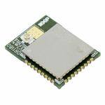
| 产品图片 |
|
| rohs | 符合RoHS无铅 / 符合限制有害物质指令(RoHS)规范要求 |
| 产品系列 | 嵌入式处理器和控制器,微控制器 - MCU,射频微控制器 - MCU,NXP Semiconductors JN5168-001-M00Z- |
| mouser_ship_limit | 此产品可能需要其他文件才能从美国出口。 |
| 数据手册 | |
| 产品型号 | JN5168-001-M00Z |
| 产品种类 | 射频微控制器 - MCU |
| 其它名称 | 568-10327-6 |
| 功率-输出 | 2.5dBm |
| 包装 | Digi-Reel® |
| 商标 | NXP Semiconductors |
| 天线连接器 | 板载,跟踪 |
| 存储容量 | 256kB 闪存, 32kB RAM, 4kB EEPROM |
| 定时器数量 | 5 Timer |
| 封装 | Reel |
| 封装/外壳 | 27-SMD 模块 |
| 工作温度 | -40°C ~ 85°C |
| 工作电源电压 | 2 V to 3.6 V |
| 工厂包装数量 | 400 |
| 应用 | RF4CE,JenNet-IP |
| 接口类型 | JTAG |
| 数据RAM大小 | 32 kB |
| 数据接口 | 用于引脚的垫片 |
| 数据速率(最大值) | - |
| 最大工作温度 | + 85 C |
| 最大时钟频率 | 400 kHz |
| 最小工作温度 | - 40 C |
| 标准包装 | 1 |
| 灵敏度 | -95dBm |
| 电压-电源 | 2 V ~ 3.6 V |
| 电流-传输 | 15mA |
| 电流-接收 | 17mA |
| 电源电压-最大 | 3.6 V |
| 电源电压-最小 | 2 V |
| 调制或协议 | 802.15.4 Zigbee |
| 频率 | 2.4GHz |


- 商务部:美国ITC正式对集成电路等产品启动337调查
- 曝三星4nm工艺存在良率问题 高通将骁龙8 Gen1或转产台积电
- 太阳诱电将投资9.5亿元在常州建新厂生产MLCC 预计2023年完工
- 英特尔发布欧洲新工厂建设计划 深化IDM 2.0 战略
- 台积电先进制程称霸业界 有大客户加持明年业绩稳了
- 达到5530亿美元!SIA预计今年全球半导体销售额将创下新高
- 英特尔拟将自动驾驶子公司Mobileye上市 估值或超500亿美元
- 三星加码芯片和SET,合并消费电子和移动部门,撤换高东真等 CEO
- 三星电子宣布重大人事变动 还合并消费电子和移动部门
- 海关总署:前11个月进口集成电路产品价值2.52万亿元 增长14.8%


PDF Datasheet 数据手册内容提取
Data Sheet: JN5168-001-Myy JenNet-IP, ZigBee PRO and IEEE802.15.4 Module Overview The JN5168-001-Myy family is a range of ultra low power, high performance surface mount Features: Module modules targeted at IEEE 802.15.4, JenNet-IP, ZigBee Light Link, ZigBee Smart Energy and • 2.4GHz IEEE 802.15.4, JenNet-IP, RF4CE networking applications, enabling users to realise products with minimum time to ZigBee Light Link, ZigBee Smart Energy market and at the lowest cost. They remove the need for expensive and lengthy development and RF4CE compatible of custom RF board designs and test suites. The modules use NXP’s JN5168 wireless microcontroller to provide a comprehensive solution with large memory, high CPU and radio • JN5168-001-M00/03 performance and all RF components included. All that is required to develop and manufacture up to 1km range (Ext antenna) wireless control or sensing products is to connect a power supply and peripherals such as M00: integral antenna 16x30mm switches, actuators and sensors, considerably simplifying product development. M03: uFl connector 16x21mm Four module variants are available: JN5168-001-M00 with an integrated antenna, JN5168-001- o TX power +2.5dBm M03 with an antenna connector and the JN5168-001-M05 and M06 with an antenna connector, o Receiver sensitivity –95dBm o TX current 15.3mA power amplifier and LNA for extended range. The JN5168-001-M05 output power has been o RX current 17mA optimised for use in Europe and Asia. o 2.0-3.6V operation Module Block Diagram • JN5168-001-M05 up to 2km range (Ext 2dBi Antenna) o 9.5 dBm TX Power o Receiver sensitivity -96dBm o uFl connector o TX current 35mA XTAL o RX current 22mA Watchdog o 16x30mm Matching Timer RAM Flash SPI Master & Slave o 2.0-3.6V operation Integrated Antenna 8/32K 64/160/256K M00 Option 2 R.4aGdHioz BVroowltangoeu t (M2-aWsitreer /SSelarivael ) • JN5168-001-M06 ConunFelc tor Matching IDnicvleurdsiintyg OM-oQdPeSmK RI3S2C - BCiPt U 4xPWM + Timers up to 6km range (Ext 2 dBi Antenna) M03 Option 2x UART o 22dBm TX Power External IEEE802.15.4 4EkEBPROM 20 DIO o Receiver sensitivity -100dBm Antenna ConunFelc tor PMA0 /5 L/MN0A6 OptioMnatching ManPaogweemrent 1A2c8cM-eblAietC rAa tEoSr 4 CShleaenp 1 C0-obuitn AteDrC ooo uTRFXXl cccuournrrrenenentct t12o72r5 mmAA AEcncceryleprtaiotonr Battery and Temp o 16x30mm Sensor o 2.0-3.6V operation Power Features: Microcontroller • 32-bit RISC CPU, up to 32MIPs with low power • Data EEPROM with guaranteed 100k write operations Benefits Applications • RF4CE, JenNet-IP, ZigBee Smart • Microminiature module solutions • Robust and secure low power wireless Energy stacks applications • Ready to use in products • JTAG debug interface • ZigBee and JenNet-IP networks • Minimises product development • 4-input 10-bit ADC, 1 comparator • Home and commercial building time automation • 5 x PWM (4 x timer, 1 x timer/counter) • No RF test required for systems • Utilities metering (e.g. AMR) • 2 UARTs • Compliant with • Location Aware services (e.g. Asset • SPI Master & Slave port with 3 selects FCC 47CFR Part 15C Tracking) • 2-wire serial interface o IC Canada RSS 210 Issue 8 - • Toys and gaming peripherals • Battery and Temperature Sensor o Annex 8, • Industrial systems • Watchdog timer and BOR o ETSI EN 300-328 V1.7.1 • Telemetry • Up to 20 DIO EN 301-489-17 V2.1.1 • Remote Control o Industrial temp (-40°C to +85°C) o EN60950-1-2006 +A1, A11, A12 Lead-free and RoHS compliant JN-DS-JN5168-001-Myy © NXP Laboratories UK 2013
Contents 1. Introduction 3 1.1. Variants 3 1.2. Regulatory Approvals 3 2. Specifications 4 2.1. JN5168 Single Chip Wireless Microcontroller 5 3. Pin Configurations 6 3.1. Pin Assignment 7 3.2. Pin Descriptions 8 3.2.1 Power Supplies 8 4. Electrical Characteristics 9 4.1. Maximum Ratings 9 4.2. Operating Conditions 9 Appendix A Additional Information 10 A.1 Outline Drawing 10 A.2 Module PCB Footprint 13 A.3 Optimal PCB placement of the JN5168-001-M00 Module 14 A.4 JN5168-001-M00 Antenna Radiation Pattern 15 A.5 Manufacturing 19 A.5.1 Reflow Profile 19 A.5.2 Soldering Paste and Cleaning 20 A.6 Tape and Reel Information 20 A.6.1 Tape Orientation and dimensions 20 A.6.2 Reel Dimensions 21 A.6.3 Cover tape details 22 A.6.4 Leader and Trailer 22 A.7 Related Documents 22 A.8 Ordering Information 23 A.9 Federal Communication Commission Interference Statement 24 A.9.1 Antennas approved by FCC for use with JN5168 modules 25 A.9.2 High Power Module usage limitation 25 A.9.3 FCC End Product Labelling 25 A.10 Industry Canada Statement 26 A.10.1 Industry Canada End Product Labelling 26 A.11 European R & TTE Directive 1999/5/EC Statement 26 A.12 RoHS Compliance 27 Status Information 27 Disclaimers 28 Trademarks 28 Version Control 28 Contact Details 29 ii JN-DS-JN5168-001-Myy 1v4 © NXP Laboratories UK 2013
1. Introduction The JN5168-001-Myy module family provides designers with a ready-made component that provides a fully integrated solution for applications, using the IEEE802.15.4 standard in the 2.4-2.5GHz ISM frequency band [1], including JenNet-IP and ZigBee Smart Energy, and can be quickly and easily included in product designs. The modules integrate all of the RF components required, removing the need to perform expensive RF design and test. Products can be designed by simply connecting sensors and switches to the module IO pins. The modules use NXP’s single chip IEEE802.15.4 Wireless Microcontroller, allowing designers to make use of the extensive chip development support material. Hence, this range of modules allows designers to bring wireless applications to market in the minimum time with significantly reduced development effort and cost. Four variants are available: JN5168-001-M00, JN5168-001-M03, JN5168-001-M05 and JN5168-001-M06. All modules have FCC and Industry Canada modular approvals. All modules other than the JN5168-001-M06 are also CE compliant and subject to a Notified Body Opinion. The variants available are described below. 1.1. Variants Variant Description FCCID Industry Canada ID JN5168-001-M00 Standard Power, integrated antenna TYOJN5168M0 7438A-CYO5168M0 JN5168-001-M03 Standard Power, uFL connector TYOJN5168M3 7438A-CYO5168M3 JN5168-001-M05 Medium Power, uFL connector TYOJN5168M5 7438A-CYO5168M5 JN5168-001-M06 High Power, uFL connector TYOJN5168M6 7438A-CYO5168M6 1.2. Regulatory Approvals The JN5168-001-M00, M03 and M05 have been tested against the requirements of the following European standards. • Radio EN 300 328 v1.7.1. • EMC, EN 301 489-17 v2.1.1 • Basic Safety Assessment (BSA) EN 60950-1:2006 A Notified Body statement of opinion for this standard is available on request. The High Power module with M06 suffix is not approved for use in Europe, instead the JN5168-001-M05 module may be used with an antenna with up to 2.2dBi; 10mW/MHz power spectral density e.i.r.p is the maximum permitted in Europe. Additionally, all module types have received FCC “Modular Approval”, in compliance with CFR 47 FCC part 15 regulations and in accordance to FCC Public notice DA00-1407. Appendix 0 contains details on the conditions applying to this modular approval. The modules are approved for use with a range of different antennas; further details of which can be found in section Appendix A.9.1. The modular approvals notice and test reports are available on request. All modules are compliant with Industry Canada RSS210 (Issue 8, Annex 8) and have Industry Canada modular approval. The JN5168-001-M06 module is subject to user proximity restrictions under FCC and Industry Canada regulations; more specific information is available in A.9.2. © NXP Laboratories UK 2013 JN-DS-JN5168-001-Myy 1v4 3
2. Specifications Most specification parameters for the modules are specified in the chip datasheet – JN-DS-JN5168 Wireless Microcontroller Datasheet [2]. Where there are differences, the parameters are defined here. VDD=3.0V @ +25°C Typical DC Characteristics Notes JN5168-001- JN5168-001- JN5168-001- M00/03 M06 M05 Deep sleep current 100nA 100nA 100nA Sleep current 0.70uA 0.70uA 0.70uA With active sleep timer Radio transmit 15.3mA 175mA 35mA CPU in doze, radio transmitting current Radio receive 17mA 22mA 22mA CPU in doze, radio receiving current Centre frequency Additional +/-15ppm allowance for +/-25ppm +/-25ppm +/-25ppm accuracy temperature and ageing Typical RF Characteristics Notes Nominal for 1% PER, as per 802.15.4 Receive sensitivity -95dBm -100dBm -96dBm section 6.5.3.3 (Note 1) Transmit power 2.5dBm 22dBm 9.5 dBm Nominal Maximum input 10dBm 5dBm 10dBm For 1% PER, measured as sensitivity signal -95 to -105 to -102 to RSSI range -10dBm -20dBm -17dBm RF Port impedance 50 ohm 50 ohm 50 ohm 2.4 - 2.5GHz – uFL connector Rx Spurious -61dBm -69dBm -69dBm Measured conducted into 50ohms Emissions Tx Spurious -40dBm -49dBm -45dBm Measured conducted into 50ohms Emissions VSWR (max) 2:1 2:1 2:1 2.4 - 2.5GHz Peripherals Notes Master SPI port 3 selects 3 selects 3 selects 250kHz - 16MHz Slave SPI port 250kHz - 4MHz Two UARTs 16550 compatible Two-wire serial I/F (compatible with Up to 400kHz SMbus & I2C) 5 x PWM (4 x timer, 16MHz clock 1 x timer/counter) Two programmable Sleep Timers 32kHz clock Digital IO lines DIO2 & DIO3 not available on JN5168-001- (multiplexed with 20 18 18 M05 and JN5168-001-M06 modules UARTs, timers and 4 JN-DS-JN5168-001-Myy 1v4 © NXP Laboratories UK 2013
SPI selects) Four channel Analogue-to-Digital 10-bit, up to 100ks/s converter Programmable analogue Ultra low power mode for sleep comparators Internal temperature sensor and battery monitor The performance of all peripherals is defined in the JN-DS-JN5168 Wireless Microcontroller Datasheet [2]. Note 1: Sensitivity is defined for conducted measurements on connectorised modules. Modules with an integrated antenna have approximately 1.5 dB less e.i.r.p and reciprocal receive sensitivity. NXP supplies all the development tools and networking stacks needed to enable end-product development to occur quickly and efficiently. These are all freely available from the NXP Wireless Connectivity TechZone: www.nxp.com/techzones/wireless-connectivity. A range of evaluation/developer kits is also available, allowing products to be quickly bread boarded. Efficient development of software applications is enabled by the provision of a complete, unlimited, software developer kit. Together with the available libraries for the IEEE802.15.4 MAC and the JenNet-IP and ZigBee PRO network stacks, this package provides everything required to develop application code and to trial it with hardware representative of the final module. The modules can be user programmed both in development and in production using software supplied by NXP. Access to the on-chip peripherals, MAC and network stack software is provided through specific APIs. This information is available on the NXP support website, together with many example applications, user guides, reference manuals and application notes. 2.1. JN5168 Single Chip Wireless Microcontroller The JN5168-001-Myy series is constructed around the JN5168-001 single chip wireless microcontroller, which includes the radio system, a 32-bit RISC CPU, Flash, RAM & EEPROM memory and a range of analogue and digital peripherals. The chip is described fully in JN-DS-JN5168 Wireless Microcontroller Datasheet [2]. © NXP Laboratories UK 2013 JN-DS-JN5168-001-Myy 1v4 5
3. Pin Configurations ADC1 1 27 VREF/ADC2 DO0 2 26 DIO17 DO1 3 25 DIO16 DIO18 4 24 DIO15 DIO19 5 23 DIO14 DIO0 6 22 RESETN DIO1 7 21 DIO13 DIO2 8 20 DIO12 DIO3 9 19 DIO11 10 11 12 13 14 15 16 17 18 4 5 6 7 8 9 0D D O O O O O O 1D N DI DI DI DI DI DI DIOV G Figure 1: Pin Configuration (top view) Note that the same basic pin configuration applies for all module designs. However, DIO3 (pin 9) and DIO2 (pin 8) are not available on the JN5168-001-M05 and JN5168-001-M06. 6 JN-DS-JN5168-001-Myy 1v4 © NXP Laboratories UK 2013
3.1. Pin Assignment Pin Pin Functions Signal Description No Primary Alternate Functions Type 1 ADC1 3.3V Analogue to Digital Input 2 DO0 SPICLK PWM2 CMOS SPI Master Clock Output or PWM2 Output 3 DO1 SPIMISO PWM3 CMOS SPI Master In Slave Out Input or PWM3 Output 4 DIO18 SPIMOSI CMOS SPI Master Out Slave In Output 5 DIO19 SPISEL0 CMSO SPI Master Select Output 0 6 DIO0 SPISEL1 ADC3 CMOS DIO0, SPI Master Select Output 1 or ADC input 3 7 DIO1 SPISEL2 ADC4 PC0 CMOS DIO1, SPI Master Select Output 2, ADC input 4 or Pulse Counter 0 Input 8 DIO2* RFRX TIM0CK_GT CMOS DIO2, Radio Receive Control Output or Timer0 Clock/Gate Input 9 DIO3* RFTX TIM0CAP CMOS DIO3, Radio Transmit Control Output or Timer0 Capture Input 10 DIO4 CTS0 JTAG_TCK TIM0OUT PC0 CMOS DIO4, UART 0 Clear To Send Input, JTAG CLK Input, Timer0 PWM Output, or Pulse Counter 0 input 11 DIO5 RTS0 JTAG_TMS PWM1 PC1 CMOS DIO5, UART 0 Request To Send Output, JTAG Mode Select Input, PWM1 Output or Pulse Counter 1 Input 12 DIO6 TXD0 JTAG_TDO PWM2 CMOS DIO6, UART 0 Transmit Data Output, JTAG Data Output or PWM2 Output 13 DIO7 RXD0 JTAG_TDI PWM3 CMOS DIO7, UART 0 Receive Data Input, JTAG Data Input or PWM 3 Output 14 DIO8 TIM0CK_GT PC1 PWM4 CMOS DIO8, Timer0 Clock/Gate Input, Pulse Counter1 Input or PWM 4 Output 15 DIO9 TIM0CAP 32KXTALIN RXD1 32KIN CMOS DIO9, Timer0 Capture Input, 32K External Crystal Input, UART 1 Receive Data Input or 32K external clock Input 16 DIO10 TIM0OUT 32KXTALOUT CMOS DIO10, Timer0 PWM Output or 32K External Crystal Output 17 VDD 3.3V Supply Voltage 18 GND 0V Digital Ground 19 DIO11 PWM1 TXD1 CMOS DIO11, PWM1 Output or UART 1 Transmit Data Output 20 DIO12 PWM2 CTS0 JTAG_TCK ADO or CMOS DIO12, PWM2 Output, UART 0 SPISMOSI Clear To Send Input, JTAG CLK Input, Antenna Diversity Odd Output or SPI Slave Master Out Slave In Input 21 DIO13 PWM3 RTS0 JTAG_TMS ADE or CMOS DIO13, PWM3 Output, UART 0 SPISMISO Request To Send Output, JTAG Mode Select Input, Antenna Diversity Even output or SPI Slave Master In Slave Out Output 22 RESETN CMOS Reset input 23 DIO14 SIF_CLK TXD0 TXD1 JTAG_TDO SPISEL1 or CMOS DIO14, Serial Interface Clock, © NXP Laboratories UK 2013 JN-DS-JN5168-001-Myy 1v4 7
SPISSEL UART 0 Transmit Data Output, UART 1 Transmit Data Output, JTAG Data Output, SPI Master Select Output 1 or SPI Slave Select Input 24 DIO15 SIF_D RXD0 RXD1 JTAG_TDI SPISEL2 CMOS DIO15, Serial Interface Data or Intelligent Peripheral Data Out 25 DIO16 COMP1P SIF_CLK SPISMOSI CMOS DIO16, Comparator Positive Input, Serial Interface clock or SPI Slave Master Out Slave In Input 26 DIO17 COMP1M PWM4 I2C DATA SPISIMO CMOS DIO17, Comparator Negative Input, Serial Interface Data or SPI Slave Master In Slave Out Output 27 VREF/ADC2 3.3V Analogue peripheral reference voltage or ADC input 2 * These two pins are not connected for JN5168-001-M05 & JN5168-001-M06 modules. 3.2. Pin Descriptions All pins behave as described in the JN-DS-JN5168 Wireless Microcontroller Datasheet [2], with the exception of the following: 3.2.1 Power Supplies A single power supply pin, VDD is provided. 8 JN-DS-JN5168-001-Myy 1v4 © NXP Laboratories UK 2013
4. Electrical Characteristics In most cases, the Electrical Characteristics are the same for both module and chip. They are described in detail in the chip datasheet. Where there are differences, they are detailed below. 4.1. Maximum Ratings Exceeding these conditions will result in damage to the device. Parameter Min Max Device supply voltage VDD -0.3V 3.6V All Pins -0.3V VDD + 0.3V Storage temperature -40ºC 150ºC 4.2. Operating Conditions Supply Min Max VDD 2.0V 3.6V Ambient temperature range -40ºC 85ºC © NXP Laboratories UK 2013 JN-DS-JN5168-001-Myy 1v4 9
Appendix A Additional Information A.1 Outline Drawing 16mm 30.0mm 1.27 mm 2.54 mm 2.54 3.30 mm mm Thickness: 3.5mm Figure 2: JN5168-001-M00 Outline Drawing 10 JN-DS-JN5168-001-Myy 1v4 © NXP Laboratories UK 2013
16mm 9.72mm 2.59 mm 1.27 mm 21mm 2.54 mm 2.54 3.30 mm mm Thickness: 3.5mm Figure 3: JN5168-001-M03 Outline Drawing © NXP Laboratories UK 2013 JN-DS-JN5168-001-Myy 1v4 11
16mm 8.0mm 2.81mm 30mm 1.27 mm 2.54 mm . 2.54 3.30 mm mm Thickness: 3.5mm Figure 4: JN5168-001-M05 and JN5168-001-M06 Outline Drawing 12 JN-DS-JN5168-001-Myy 1v4 © NXP Laboratories UK 2013
A.2 Module PCB Footprint All dimensions are in mm. 16.00 1.27 Ø1 2.54 1.5 2.54 3.30 1 Note: All modules have the same footprint Figure 5: Module PCB footprint © NXP Laboratories UK 2013 JN-DS-JN5168-001-Myy 1v4 13
A.3 Optimal PCB placement of the JN5168-001-M00 Module The JN5168-001-M00 module features an optimised, low cost, integrated, inverted F, printed PCB antenna. The antenna has a vertically polarised near omnidirectional radiation pattern and up to 1.6 dBi of peak gain. The PCB design has been elongated in order to increase the ground plane area which increases the antenna efficiency. This allows stand alone operation without any additional ground plane however care must be taken when mounting this module onto another PCB. The area around the antenna must be kept clear of conductors or other metal objects for an absolute minimum of 20 mm. This is true for all layers of the PCB and not just the top layer. Any conductive objects close to the antenna could severely disrupt the antenna pattern resulting in deep nulls and high directivity in some directions. The diagrams below show various possible scenarios. The top 3 scenarios are correct; groundplane may be placed beneath JN5168-001-M00 module as long as it does not protrude beyond the edge of the top layer ground plane on the module PCB. The bottom 3 scenarios are incorrect; the left hand side example because there is groundplane underneath the antenna, the middle example because there is insufficient clearance around the antenna (it is best to have no conductors anywhere near the antenna), finally the right hand example has a battery’s metal casing in the recommended keep out area. Figure 6: PCB placement of the JN5168-001-M00 Module 14 JN-DS-JN5168-001-Myy 1v4 © NXP Laboratories UK 2013
A.4 JN5168-001-M00 Antenna Radiation Pattern Figure 7, Figure 8 & Figure 9 are simulated 3D radiation plots of the JN5168-001-M00. They are provided here to help the user orientate the module in end equipment in an optimal way. These visualisations are an accurate representation of the antenna radiation pattern in the 3D space. The 2D XZ plots for each channel are shown in JN5168-001-M00 Radiation Plots @ 3 meters (XZ Orientation) dBuV CH11 CH18 CH26 104 94 2 84 3 1 74 64 54 44 34 24 14 4 14 24 34 44 54 64 74 84 94 104 Mkr Trace X-Axis Value 1 CH11 40.0 deg 101.04 dBuV 2 CH18 40.0 deg 100.67 dBuV 3 CH26 40.0 deg 101.26 dBuV Figure 10. These are actual measurements in an anechoic chamber with the JN5168-001-M00 mounted on a DR1174 carrier board from the JN516x-EK001 Evaluation kit. The device under test and the antenna height was 1m and the values are in dBuV/m at a distance of 3m. Figure 11 is a plot of the peak field strengths for a JN5168-001-M00, JN5148-001-M00 and JN5168-001-M03. The M03 is used with a λ/2 vertical antenna. Figure 11 shows that the new integrated antenna is 1.5-3dB better than the JN5148-001-M00 and is within 1.5 dB of a JN5168-001-M03 λ/2 vertical. © NXP Laboratories UK 2013 JN-DS-JN5168-001-Myy 1v4 15
Figure 7: 3D radiation plot JN5168-001-M00 XY Orientation (simulation) Figure 8: 3D radiation plot JN5168-001-M00 XZ Orientation (simulation) 16 JN-DS-JN5168-001-Myy 1v4 © NXP Laboratories UK 2013
Figure 9: 3D radiation plot JN5168-001-M00 YZ Orientation (simulation) © NXP Laboratories UK 2013 JN-DS-JN5168-001-Myy 1v4 17
JN5168-001-M00 Radiation Plots @ 3 meters (XZ Orientation) dBuV CH11 CH18 CH26 104 94 2 84 3 1 74 64 54 44 34 24 14 4 14 24 34 44 54 64 74 84 94 104 Mkr Trace X-Axis Value 1 CH11 40.0 deg 101.04 dBuV 2 CH18 40.0 deg 100.67 dBuV 3 CH26 40.0 deg 101.26 dBuV Figure 10: Actual radiation plot of JN5168-001-M00 Mounted on a carrier PCB – XZ orientation 18 JN-DS-JN5168-001-Myy 1v4 © NXP Laboratories UK 2013
Module Peak Field Strengths 104.0 103.5 103.0 m 102.5 3102.0 JN5168-001-M03 with @ 101.5 vertical m 101.0 V/100.5 JN5168-001-M00 Bu100.0 d 99.5 99.0 JN5148-001-M00 98.5 98.0 11 18 26 Channel Figure 11: Peak Field Strengths for various modules optimised for height and azimuth A.5 Manufacturing A.5.1 Reflow Profile For reflow soldering, it is recommended to follow the reflow profile in figure 6 as a guide, as well as the paste manufacturer’s guidelines on peak flow temperature, soak times, time above liquid and ramp rates. Temperature 25~160 ºC 160~190 ºC > 220º C 230~Pk. Pk. Temp (235ºC) Target Time (s) 90~130 30~60 20~50 10~15 150~270 Figure 12: Recommended solder reflow profile © NXP Laboratories UK 2013 JN-DS-JN5168-001-Myy 1v4 19
A.5.2 Soldering Paste and Cleaning NXP does not recommend use of a solder paste that requires the module and PCB assembly to be cleaned (rinsed in water) for the following reasons: Solder flux residues and water can be trapped by the PCB, can or components and result in short circuits. The module label could be damaged or removed. NXP recommends use of a 'no clean' solder paste for all its module products. A.6 Tape and Reel Information A.6.1 Tape Orientation and dimensions All dimensions are in mm. Module type A B W F E P0 P1 P2 T Cover Tape width (W) JN5168-001-M00 16.6 30.6 44 20.2 1.75 4.0 24.0 2.0 3.7 44.0 JN5168-001-M03 16.6 21.6 44 20.2 1.75 4.0 24.0 2.0 3.7 44.0 JN5168-001-M05 16.6 30.6 44 20.2 1.75 4.0 24.0 2.0 3.7 44.0 JN5168-001-M06 16.6 30.6 44 20.2 1.75 4.0 24.0 2.0 3.7 44.0 Tolerance ±0.1 ±0.1 ±0.3 ±0.15 +0.1 ±0.1 ±0.1 ±0.15 ±0.1 ±0.3 20 JN-DS-JN5168-001-Myy 1v4 © NXP Laboratories UK 2013
A.6.2 Reel Dimensions All dimensions are in mm. Module A B N W1 W2 (Max) JN5168-001-MYY 330 ±2.0 2.0±0.5 181.3±0.2 45.0 +1.4/-0.6 50.4 © NXP Laboratories UK 2013 JN-DS-JN5168-001-Myy 1v4 21
A.6.3 Cover tape details Thickness (T) 0.06 ± 0.005mm Width (W) 37.5 ± 0.1mm Surface resistivity (component side) 105 to 1011 Ohms/sq Surface resistivity (component side) Non-conductive Backing type: Polyester Adhesive type: PSA Sealing: Room ambient A.6.4 Leader and Trailer Vacant Quantity/400PCS Vacant >500mm >500 MM A.7 Related Documents [1] IEEE Std 802.15.4-2003 IEEE Standard for Information Technology – Part 15.4 Wireless Medium Access Control (MAC) and Physical Layer (PHY) Specifications for Low-Rate Wireless Personal Area Networks (LR-WPANs) [2] JN-DS-JN5168 Wireless Microcontroller Datasheet 22 JN-DS-JN5168-001-Myy 1v4 © NXP Laboratories UK 2013
A.8 Ordering Information Ordering Code Format: JN5168-001-MYY Module Type (YY) 00 Standard Power, Integral antenna 03 Standard Power, uFl connector 05 Medium Power, uFL connector 06 High Power, uFl connector Where this Data Sheet is denoted as “Advanced” or “Preliminary”, devices will be either Engineering Samples or Prototypes. Part Number Description JN5168-001-M00 Shipped in tape mounted 400 piece reel JN5168-001-M03 JN5168-001-M05 JN5168-001-M06 Line Content Format Options Sample 1 NXP Logo B&W outline logo 1 2D 2D Matrix Symbology, square Coding data matrix ECC-200 with 0.5mm cell size JN5168-001-M00 2 Part ID JN5168-001-M0x x is module type, 0, 3, 5 or 6 NNNNN 3 Serial No. NNNNN Serial number from test ZSDYWW 4 Z SSMC FCC ID:TYOJN5168M0 S APK D RoHs IC:7438A-CYO5168M0 Compliant Y Year WW Week 5 FCC ID FCCID:TYOJN5168Mx x is module type 0,3,5 or 6 6 IC ID IC:7438A- x is module type CYO5168Mx 0,3,5 or 6 Figure 13: Example module labelling Note :- The 2-D barcode in line 1 is used only for production purposes. © NXP Laboratories UK 2013 JN-DS-JN5168-001-Myy 1v4 23
A.9 Federal Communication Commission Interference Statement This equipment has been tested and found to comply with the limits for a Class B digital device, pursuant to Part 15 of the FCC Rules. These limits are designed to provide reasonable protection against harmful interference in a residential installation. This equipment generates, uses, and can radiate radio frequency energy and, if not installed and used in accordance with the instructions, may cause harmful interference to radio communications. However, there is no guarantee that interference will not occur in a particular installation. If this equipment does cause harmful interference to radio or television reception, which can be determined by turning the equipment off and on, the user is encouraged to try to correct the interference by one of the following measures: - Reorient or relocate the receiving antenna. - Increase the separation between the equipment and receiver. - Connect the equipment into an outlet on a circuit different from that to which the receiver is connected. - Consult the dealer or an experienced radio/TV technician for help. This device complies with Part 15 of the FCC Rules. Operation is subject to the following two conditions: (1) This device may not cause harmful interference, and (2) this device must accept any interference received, including interference that may cause undesired operation. FCC Caution: Any changes or modifications not expressly approved by the party responsible for compliance could void the user's authority to operate this equipment. WARNING! FCC Radiation Exposure Statement: This portable equipment with its antenna complies with FCC’s RF radiation exposure limits set forth for an uncontrolled environment. To maintain compliance follow the instructions below; 1. This transmitter must not be co-located or operating in conjunction with any other antenna or transmitter. 2. Avoid direct contact to the antenna, or keep it to a minimum while using this equipment. This transmitter module is authorized to be used in other devices only by OEM integrators under the following condition: The transmitter module must not be co-located with any other antenna or transmitter. As long as the above condition is met, further transmitter testing will not be required. However, the OEM integrator is still responsible for testing their end product for any additional compliance requirements required with this module installed (for example, digital device emissions, PC peripheral requirements, etc.). This applies to the JN5168-001-M00, JN5168-001-M03 and JN5168-001-M05 devices, the JN5168-001-M06 is a mobile device (see section A.9.2) 24 JN-DS-JN5168-001-Myy 1v4 © NXP Laboratories UK 2013
A.9.1 Antennas approved by FCC for use with JN5168 modules Brand Model Number Description Gain (dBi) Connector type 1 Antenna Factor ANT-2.4-CW-RCT-RP Vertical - knuckle antenna 2.2 RP-SMA 2 Antennova 2010B6090-01 Vertical - knuckle antenna 2.2 RP-SMA 3 Hyperlink Technology HG2402RD-RSF Vertical - knuckle antenna 2.2 RP-SMA 4 Aveslink Technology, Inc E-0005-AC Vertical- flying lead 2 RP-SMA 5 Aveslink Technology, Inc E-2411-GC Vertical - swivel 2 RP-SMA 6 Aveslink Technology, Inc E-2410-CA Vertical - bulkhead- flying lead 2 uFL 7 Aveslink Technology, Inc E-2410-GC Vertical - swivel 2 RP-SMA 8 Aveslink Technology, Inc E-2820-CA Vertical - bulkhead- flying lead 2 uFL 9 Aveslink Technology, Inc E-2820-GC Vertical - swivel 2 RP-SMA 10 Embedded Antenna Design FBKR35068-RS-KR Vertical - knuckle antenna 2 RP-SMA 11 Nearson S131CL-L-PX-2450S Vertical - knuckle-flying lead 2 uFL 12 Laird Technologies WRR2400-IP04 Vertical - knuckle-flying lead 1.5 uFL 13 Laird Technologies WRR2400-RPSMA Vertical - knuckle-flying lead 1.3 RP-SMA 14 Aveslink Technology, Inc E-6170-DA Vertical - right angle 1 uFL 15 Laird Technologies WCR2400-SMRP Vertical - knuckle antenna 1 RP-SMA This device has been designed to operate with the antennas listed above, and having a maximum gain of 2.2 dBi. Alternative vertical antennas may be used provided that the gain does not exceed 2.2 dBi. Antennas having a gain greater than 2.2 dBi are strictly prohibited for use with this device. The required antenna impedance is 50 ohms. A.9.2 High Power Module usage limitation The high power module variants are classified as ‘mobile’ device pursuant with FCC § 2.1091 and must not be used at a distance of < 20 cm (8”) from any people. This applies to the JN5168-001-M06 module type (TYOJN5168M6). IMPORTANT NOTE: In the event that these conditions cannot be met (for certain configurations or co-location with another transmitter), then the FCC authorization is no longer considered valid and the FCC ID can not be used on the final product. In these circumstances, the OEM integrator will be responsible for re-evaluating the end product (including the transmitter) and obtaining a separate FCC authorization. The OEM integrator has to be aware not to provide information to the end user regarding how to install or remove this RF module in the user manual of the end product. The user manual for the end product must include the following information in a prominent location; “To comply with FCC’s RF radiation exposure requirements, the antenna(s) used for this transmitter must not be co- located or operating in conjunction with any other antenna or transmitter.” A.9.3 FCC End Product Labelling The final ‘end product’ should be labelled in a visible area with the following: “Contains TX FCC ID: TYOJN5168M0, TYOJN5168M3, TYOJN5168M5 or TYOJN5168M6” to reflect the version of the module being used inside the product. © NXP Laboratories UK 2013 JN-DS-JN5168-001-Myy 1v4 25
A.10 Industry Canada Statement This device complies with Industry Canada licence- Le présent appareil est conforme aux CNR d'Industrie exempt RSS standard(s). Operation is subject Canada applicables aux appareils radio to the following two conditions: (1) this device may exempts de licence. L'exploitation est autorisée aux not cause interference, and (2) this device must deux conditions suivantes : (1) l'appareil ne accept any interference, including interference that doit pas produire de brouillage, et (2) l'utilisateur de may cause undesired operation of the device. l'appareil doit accepter tout brouillage radioélectrique subi, même si le brouillage est susceptible d'en compromettre le fonctionnement. To reduce potential radio interference to other users, the antenna type and its gain should be so chosen that the equivalent isotropic radiated power (e.i.r.p.) is not more than that permitted for successful communication. These modules have been designed to operate with antennas having a maximum gain of 2.2 dBi. Antennas having a gain greater than 2.2 dBi are strictly prohibited for use with this device. The required antenna impedance is 50 ohms. As long as the above condition is met, further transmitter testing will not be required. However, the OEM integrator is still responsible for testing their end-product for any additional compliance requirements required with this module installed (for example, digital device emissions, PC peripheral requirements, etc). A.10.1 Industry Canada End Product Labelling For Industry Canada purposes the following should be used. “Contains Industry Canada ID IC: 7438A-CYO5168M0, IC: 7438A-CYO5168M3, IC: 7438A-CYO5168M5 or IC: 7438A-CYO5168M6” to reflect the version of the module being used inside the product. A.11 European R & TTE Directive 1999/5/EC Statement All modules listed in this datasheet with the exception of the JN5168-001-M06 are compliant with ETSI EN 300 328 V1.7.1 (2006-10), EMC, EN 301 489-17 v2.1.1 (2009-02) and the Basic Safety Assessment (BSA) EN 60950-1:2006 (2006-06) and are subject to a Notified Body Opinion. The modules are approved for use with the antennas listed in the following table. The JN5168-001-M06 module is not approved for use in Europe, instead use the JN5168-001-M05 which produces the maximum permitted power. Alternative vertical antennas may be used provided that the gain does not exceed 2.2 dBi. Brand Model Number Description Gain (dBi) Connector type 1 Antenna Factor ANT-2.4-CW-RCT-SMA Vertical - knuckle antenna 2.2 SMA 2 Antennova B6090 Vertical - knuckle antenna 2.2 RP-SMA 3 Hyperlink Technology HG2402RD-RSF Vertical - knuckle antenna 2.2 RP-SMA 4 Aveslink Technology, Inc E-0005-AC Vertical- flying lead 2 RP-SMA 5 Aveslink Technology, Inc E-2411-GC Vertical - swivel 2 RP-SMA 6 Aveslink Technology, Inc E-2410-CA Vertical - bulkhead- flying lead 2 uFL 7 Aveslink Technology, Inc E-2410-GC Vertical - swivel 2 RP-SMA 8 Aveslink Technology, Inc E-2820-CA Vertical - bulkhead- flying lead 2 uFL 9 Aveslink Technology, Inc E-2820-GC Vertical - swivel 2 RP-SMA 10 Embedded Antenna Design FBKR35068-RS-KR Vertical - knuckle antenna 2 RP-SMA 11 Nearson S131CL-L-PX-2450S Vertical - knuckle-flying lead 2 uFL 12 Laird Technologies WRR2400-IP04 Vertical - knuckle-flying lead 1.5 uFL 13 Laird Technologies WRR2400-RPSMA Vertical - knuckle-flying lead 1.3 RP-SMA 14 Aveslink Technology, Inc E-6170-DA Vertical - right angle 1 uFL 15 Laird Technologies WCR2400-SMRP Vertical - knuckle antenna 1 RP-SMA 26 JN-DS-JN5168-001-Myy 1v4 © NXP Laboratories UK 2013
A.12 RoHS Compliance JN5168-001-Myy modules meet the requirements of Directive 2002/95/EC of the European Parliament and of the Council on the Restriction of Hazardous Substance (RoHS) and of the Chinese RoHS requirements SJ/T11363-2006 which came into force on 1st March 2007. Status Information The status of this Data Sheet is Production. NXP products progress according to the following format: Advanced The Data Sheet shows the specification of a product in planning or in development. The functionality and electrical performance specifications are target values and may be used as a guide to the final specification. NXP reserves the right to make changes to the product specification at anytime without notice. Preliminary The Data Sheet shows the specification of a product that is commercially available, but is not yet fully qualified. The functionality of the product is final. The electrical performance specifications are target values and may be used as a guide to the final specification. NXP reserves the right to make changes to the product specification at anytime without notice. Production This is the production Data Sheet for the product. All functional and electrical performance specifications, where included, including min and max values are derived from detailed product characterization. This Data Sheet supersedes all previous document versions. NXP reserves the right to make changes to the product specification at anytime. © NXP Laboratories UK 2013 JN-DS-JN5168-001-Myy 1v4 27
Disclaimers Limited warranty and liability — Information in this document is believed to be accurate and reliable. However, NXP Semiconductors does not give any representations or warranties, expressed or implied, as to the accuracy or completeness of such information and shall have no liability for the consequences of use of such information. NXP Semiconductors takes no responsibility for the content in this document if provided by an information source outside of NXP Semiconductors. In no event shall NXP Semiconductors be liable for any indirect, incidental, punitive, special or consequential damages (including - without limitation - lost profits, lost savings, business interruption, costs related to the removal or replacement of any products or rework charges) whether or not such damages are based on tort (including negligence), warranty, breach of contract or any other legal theory. Notwithstanding any damages that customer might incur for any reason whatsoever, NXP Semiconductors’ aggregate and cumulative liability towards customer for the products described herein shall be limited in accordance with the Terms and conditions of commercial sale of NXP Semiconductors. Right to make changes — NXP Semiconductors reserves the right to make changes to information published in this document, including without limitation specifications and product descriptions, at any time and without notice. This document supersedes and replaces all information supplied prior to the publication hereof. Suitability for use — NXP Semiconductors products are not designed, authorized or warranted to be suitable for use in life support, life-critical or safety-critical systems or equipment, nor in applications where failure or malfunction of an NXP Semiconductors product can reasonably be expected to result in personal injury, death or severe property or environmental damage. NXP Semiconductors and its suppliers accept no liability for inclusion and/or use of NXP Semiconductors products in such equipment or applications and therefore such inclusion and/or use is at the customer’s own risk. Applications — Applications that are described herein for any of these products are for illustrative purposes only. NXP Semiconductors makes no representation or warranty that such applications will be suitable for the specified use without further testing or modification. Customers are responsible for the design and operation of their applications and products using NXP Semiconductors products, and NXP Semiconductors accepts no liability for any assistance with applications or customer product design. It is customer’s sole responsibility to determine whether the NXP Semiconductors product is suitable and fit for the customer’s applications and products planned, as well as for the planned application and use of customer’s third party customer(s). Customers should provide appropriate design and operating safeguards to minimize the risks associated with their applications and products. NXP Semiconductors does not accept any liability related to any default, damage, costs or problem which is based on any weakness or default in the customer’s applications or products, or the application or use by customer’s third party customer(s). Customer is responsible for doing all necessary testing for the customer’s applications and products using NXP Semiconductors products in order to avoid a default of the applications and the products or of the application or use by customer’s third party customer(s). NXP does not accept any liability in this respect. Export control — This document as well as the item(s) described herein may be subject to export control regulations. Export might require a prior authorization from competent authorities. Limiting values — Stress above one or more limiting values (as defined in the Absolute Maximum Ratings System of IEC 60134) will cause permanent damage to the device. Limiting values are stress ratings only and (proper) operation of the device at these or any other conditions above those given in the Operating Conditions section or the Electrical Characteristics sections of this document is not warranted. Constant or repeated exposure to limiting values will permanently and irreversibly affect the quality and reliability of the device. AEC unqualified products — This product has not been qualified to the appropriate Automotive Electronics Council (AEC) standard Q100 or Q101 and should not be used in automotive applications, including but not limited to applications where failure or malfunction of an NXP Semiconductors product can reasonably be expected to result in personal injury, death or severe property or environmental damage. NXP Semiconductors accepts no liability for inclusion and/or use of NXP Semiconductors products in such equipment or applications and therefore such inclusion and/or use is for the customer’s own risk. Product specification — The information and data provided in a Product data sheet shall define the specification of the product as agreed between NXP Semiconductors and its customer, unless NXP Semiconductors and customer have explicitly agreed otherwise in writing. In no event however, shall an agreement be valid in which the NXP Semiconductors product is deemed to offer functions and qualities beyond those described in the Product data sheet All products are sold subject to NXP Semiconductors’ terms and conditions of sale, supplied at the time of order acknowledgment and published at http://www.nxp.com/profile/terms. Trademarks All trademarks are the property of their respective owners. “JenNet” and “JenNet-IP” are trademarks of NXP B.V.. Version Control Version Notes 1.0 Initial release 1.1 Additional clarification of RF exposure conditions added to FCC Section A8 and minor corrections made 1.2 Revision of key parameters. Module footprint dimension updated 1.3 Tape and reel information added 1.4 Updated pin configuration and assignments. Module labelling and reel dimensions updated. 28 JN-DS-JN5168-001-Myy 1v4 © NXP Laboratories UK 2013
Contact Details NXP Laboratories UK Ltd Furnival Street Sheffield S1 4QT United Kingdom Tel: +44 (0)114 281 2655 Fax: +44 (0) 114 281 2951 For the contact details of your local NXP office or distributor, refer to the NXP web site: www.nxp.com © NXP Laboratories UK 2013 JN-DS-JN5168-001-Myy 1v4 29
Mouser Electronics Authorized Distributor Click to View Pricing, Inventory, Delivery & Lifecycle Information: N XP: JN5168-001-M00Z JN5168-001-M03Z JN5168-001-M05Z JN5168-001-M06Z