ICGOO在线商城 > ITS4142N
 Datasheet下载
- 型号: ITS4142N
- 制造商: Infineon
- 库位|库存: xxxx|xxxx
- 要求:
| 数量阶梯 | 香港交货 | 国内含税 |
| +xxxx | $xxxx | ¥xxxx |
查看当月历史价格
查看今年历史价格
ITS4142N产品简介:
ICGOO电子元器件商城为您提供ITS4142N由Infineon设计生产,在icgoo商城现货销售,并且可以通过原厂、代理商等渠道进行代购。 提供ITS4142N价格参考以及InfineonITS4142N封装/规格参数等产品信息。 你可以下载ITS4142N参考资料、Datasheet数据手册功能说明书, 资料中有ITS4142N详细功能的应用电路图电压和使用方法及教程。
| 参数 | 数值 |
| 产品目录 | 集成电路 (IC)半导体 |
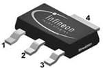
| 描述 | IC SWITCH HISIDE SMART SOT223-4电源开关 IC - 配电 SMART HI SIDE SWITCH INDUSTRIAL APPS |
| 产品分类 | PMIC - MOSFET,电桥驱动器 - 内部开关集成电路 - IC |
| 品牌 | Infineon Technologies |
| 产品手册 | http://www.infineon.com/dgdl/ITS4142N_20060309.pdf?folderId=db3a304412b407950112b408e8c90004&fileId=db3a304412b407950112b4296b0840e1&sId=db3a30443a06def4013a0707fd70004b |
| 产品图片 |
|
| rohs | 符合RoHS无铅 / 符合限制有害物质指令(RoHS)规范要求 |
| 产品系列 | 开关 IC,电源开关 IC - 配电,Infineon Technologies ITS4142NminiPROFET® |
| 数据手册 | http://www.infineon.com/dgdl/Infineon-ITS4142N_20060309-DS-v01_01-en.pdf?folderId=db3a304412b407950112b408e8c90004&fileId=db3a304412b407950112b4296b0840e1&ack=t |
| 产品型号 | ITS4142N |
| 产品目录页面 | |
| 产品种类 | 电源开关 IC - 配电 |
| 供应商器件封装 | PG-SOT223-4 |
| 其它名称 | ITS4142NDKR |
| 包装 | Digi-Reel® |
| 商标 | Infineon Technologies |
| 安装类型 | 表面贴装 |
| 安装风格 | SMD/SMT |
| 导通电阻 | 150 毫欧 |
| 导通电阻—最大值 | 0.15 Ohms |
| 封装 | Reel |
| 封装/外壳 | TO-261-4,TO-261AA |
| 封装/箱体 | SOT-223-4 |
| 工作温度 | -30°C ~ 85°C |
| 工作电源电压 | 12 V to 45 V |
| 工厂包装数量 | 4000 |
| 最大功率耗散 | 1400 mW |
| 最大工作温度 | + 85 C |
| 最大输入电压 | 45 V |
| 最小工作温度 | - 30 C |
| 最小输入电压 | 12 V |
| 标准包装 | 1 |
| 电压-电源 | 12 V ~ 45 V |
| 电流-峰值输出 | 3A |
| 电流-输出/通道 | 1.4A |
| 电源电流—最大值 | 1 mA |
| 类型 | 高端 |
| 系列 | ITS4142 |
| 输入类型 | 非反相 |
| 输出数 | 1 |
| 输出电流 | 1.4 A |
| 输出端数量 | 1 Output |
| 零件号别名 | ITS4142NHUMA1 SP000221218 |


- 商务部:美国ITC正式对集成电路等产品启动337调查
- 曝三星4nm工艺存在良率问题 高通将骁龙8 Gen1或转产台积电
- 太阳诱电将投资9.5亿元在常州建新厂生产MLCC 预计2023年完工
- 英特尔发布欧洲新工厂建设计划 深化IDM 2.0 战略
- 台积电先进制程称霸业界 有大客户加持明年业绩稳了
- 达到5530亿美元!SIA预计今年全球半导体销售额将创下新高
- 英特尔拟将自动驾驶子公司Mobileye上市 估值或超500亿美元
- 三星加码芯片和SET,合并消费电子和移动部门,撤换高东真等 CEO
- 三星电子宣布重大人事变动 还合并消费电子和移动部门
- 海关总署:前11个月进口集成电路产品价值2.52万亿元 增长14.8%


PDF Datasheet 数据手册内容提取
ITS 4142N Smart High-Side Power Switch for Industrial Applications Ω 1 Channel: 1 x 200m Features Product Summary • Short circuit protection Overvoltage protection V 47 V bb(AZ) • Current limitation Operating voltage V 12...45 V bb(on) • Overload protection On-state resistance R 200 mΩ ON • Overvoltage protection Operating temperature T -30...+85 (cid:176)C a (including load dump) • Undervoltage shutdown with auto- restart and hysteresis • Switching inductive loads • Clamp of negative voltage at output with inductive loads • CMOS compatible input PG-SOT223 • Thermal shutdown with restart • ESD - Protection • Loss of GND and loss of V protection bb • Very low standby current • Reverse battery protection with external resistor • Improved electromagnetic compatibility (EMC) Application • All types of resistive, inductive and capacitive loads • (cid:181)C compatible power switch for 12 V and 24 V DC industrial applications • Replaces electromechanical relays and discrete circuits General Description N channel vertical power FET with charge pump, ground referenced CMOS compatible input, monolithically integrated in Smart SIPMOS technology. Providing embedded protective functions. 2006-03-09 Page 1
ITS 4142N Block Diagram + Vbb 4 Voltage Overvoltage Current Gate source protection limit protection V Logic Voltage Charge pump Limit for OUT unclamped 1 sensor Level shifter ind. loads Temperature sensor Rectifier R 3 in IN Load ESD Logic miniPROFETfi GND 2 Signal GND Load GND Pin Symbol Function 1 OUT Output to the load 2 GND Logic ground 3 IN Input, activates the power switch in case of logic high signal 4 Vbb Positive power supply voltage 2006-03-09 Page 2
ITS 4142N Maximum Ratings Parameter Symbol Value Unit at T = 25(cid:176)C, unless otherwise specified j Supply voltage V -0,31)...48 V bb Continuous input voltage2) V -10...V IN bb Load current (Short - circuit current, see page 5) I self limited A L Current through input pin (DC) I ±5 mA IN Reverse current through GND-pin3) -I -0.5 A GND Junction temperature T internal limited (cid:176)C j Operating temperature Ta -30...+85 (cid:176)C Storage temperature T -40 ... +105 (cid:176)C stg Power dissipation 4) P 1.4 W tot Inductive load switch-off energy dissipation4)5) E 0.16 J AS single pulse T = 125 (cid:176)C, I = 1 A j L Load dump protection5) V 6)= V + V V V LoadDump A S Loaddump R=2Ω, t =400ms, V = low or high, V =13,5V I d IN A R = 47 Ω 83 L Electrostatic discharge voltage (Human Body Model) VESD kV according to ANSI EOS/ESD - S5.1 - 1993 ESD STM5.1 - 1998 Input pin ±1 All other pins ±5 1defined by Ptot 2At VIN > Vbb, the input current is not allowed to exceed –5 mA. 3defined by Ptot 4Device on 50mm*50mm*1.5mm epoxy PCB FR4 with 6 cm2 (one layer, 70(cid:181)m thick) copper area for Vbb connection. PCB is vertical without blown air. 5not subject to production test, specified by design 6VLoaddump is setup without the DUT connected to the generator per ISO 7637-1 and DIN 40839 . Supply voltages higher than Vbb(AZ) require an external current limit for the GND pin, e.g. with a 150Ω resistor in GND connection. A resistor for the protection of the input is integrated. 2006-03-09 Page 3
ITS 4142N Electrical Characteristics Parameter Symbol Values Unit at T = -40...125 (cid:176)C, V = 15...30 V unless otherwise specified min. typ. max. j bb Thermal Characteristics Thermal resistance @ min. footprint R - - 125 K/W th(JA) Thermal resistance @ 6 cm2 cooling area 1) R - - 70 th(JA) Thermal resistance, junction - soldering point R - - 7 K/W thJS Load Switching Capabilities and Characteristics On-state resistance R mΩ ON T = 25 (cid:176)C, I = 0.5 A - 150 200 j L T = 125 (cid:176)C - 270 320 j Nominal load current2) I 1.4 - - A L(nom) Device on PCB 1) Turn-on time to 90% VOUT ton (cid:181)s R = 47 Ω, V = 0 to 10 V - 50 100 L IN Turn-off time to 10% VOUT toff R = 47 Ω, V = 10 to 0 V - 75 150 L IN Slew rate on 10 to 30% V , dV/dt V/(cid:181)s OUT on R = 47 Ω, V = 15 V - 1 2 L bb Slew rate off 70 to 40% V , -dV/dt OUT off R = 47 Ω, V = 15 V - 1 2 L bb 1Device on 50mm*50mm*1.5mm epoxy PCB FR4 with 6 cm2 (one layer, 70(cid:181)m thick) copper area for Vbb connection. PCB is vertical without blown air. 2Nominal load current is limited by the current limitation ( see page 5 ) 2006-03-09 Page 4
ITS 4142N Electrical Characteristics Parameter Symbol Values Unit at T = -40...125 (cid:176)C, V = 15...30 V unless otherwise specified min. typ. max. j bb Operating Parameters Operating voltage V 12 - 45 V bb(on) Undervoltage shutdown V 7 - 10.5 bb(under) Undervoltage restart V - - 11 bb(u rst) Undervoltage hysteresis ∆V - 0.5 - bb(under) ∆V = V - V bb(under) bb(u rst) bb(under) Standby current I (cid:181)A bb(off) T = -40...85 (cid:176)C, V ≤ 1,2 V - 10 25 j IN T = 125 (cid:176)C1) - - 50 j Operating current I - 1 1.6 mA GND Leakage output current (included in Ibb(off)) IL(off) - 3.5 10 (cid:181)A V ≤ 1,2 V IN Protection Functions2) Initial peak short circuit current limit I A L(SCp) T = -40 (cid:176)C, V = 20 V, t = 150 (cid:181)s - - 4.5 j bb m T = 25 (cid:176)C - 3 - j T = 125 (cid:176)C 1.4 - - j Repetitive short circuit current limit I - 2.2 - L(SCr) T = T (see timing diagrams) j jt Output clamp (inductive load switch off) V 62 68 - V ON(CL) at V = V - V , I = 4 mA OUT bb ON(CL) bb Overvoltage protection 3) V 47 - - bb(AZ) I = 4 mA bb Thermal overload trip temperature4) T 135 - - (cid:176)C jt Thermal hysteresis ∆T - 10 - K jt 1higher current due temperature sensor 2Integrated protection functions are designed to prevent IC destruction under fault conditions described in the data sheet. Fault conditions are considered as "outside" normal operating range. Protection functions are not designed for continuous repetitive operation. 3see also VON(CL) in circuit diagram 4 higher operating temperature at normal function available 2006-03-09 Page 5
ITS 4142N Electrical Characteristics Parameter Symbol Values Unit at T = -40...125 (cid:176)C, V = 15...30 V unless otherwise specified min. typ. max. j bb Input Continuous input voltage1) V -102) - V V IN bb Input turn-on threshold voltage V - - 3.0 IN(T+) Input turn-off threshold voltage V 1.82 - - IN(T-) Input threshold hysteresis ∆V - 0.2 - IN(T) Off state input current I (cid:181)A IN(off) V ≤ 1,8 V 20 - - IN On state input current I - - 110 IN(on) Input delay time at switch on V t 150 340 - (cid:181)s bb d(Vbbon) Input resistance (see page 8) R 1.5 3 5 kΩ I Reverse Battery Reverse battery voltage3)2) -V V bb R = 0 Ω - - 0.3 GND R = 150 Ω - - 45 GND Continuous reverse drain current2) I - - 1 A S T = 25 (cid:176)C j Drain-source diode voltage (V > V ) -V - 0.6 1.2 V OUT bb ON I = 1 A F 1At VIN > Vbb, the input current is not allowed to exceed –5 mA. 2not subject to production test, guaranted by design 3defined by Ptot 2006-03-09 Page 6
ITS 4142N EMC-Characteristics All EMC-Characteristics are based on limited number of sampels and no part of production test. Test Conditions: If not other specified the test circuitry is the minimal functional configuration without any external components for protection or filtering. Supply voltage: V = 13.5V Temperature: T = 23 ±5(cid:176)C ; bb a Load: R = 220Ω L Operation mode: PWM Frequency: 100Hz / Duty Cycle: 50% DC On/Off DUT-Specific.: R GND Fast electrical transients Acc. ISO 7637 Test Pulse Test Level Test Results Pulse Cycle Time and On Off Generator Impedance 1 -200 V C C 500ms ; 10Ω 2 +200 V C C 500ms ; 10Ω 3a -200 V C C 100ms ; 50Ω 3b + 200 V C C 100ms ; 50Ω 41) -7 V C C 0,01Ω 5 175 V E (70V) E (70V) 400ms ; 2Ω The test pulses are applied at Vbb Definition of functional status Class Content C All functions of the device are performed as designed after exposure to disturbance. E One or more function of a device does not perform as designed after exposure and can not be returned to proper operation without repairing or replacing the device. The value after the character shows the limit. Test circuit: Pulse Bat. Vbb IN PROFET OUT GND R L R GND 1Supply voltage Vbb = 12 V instead of 13,5 V. 2006-03-09 Page 7
ITS 4142N Conducted Emission Acc. IEC 61967-4 (1Ω / 150Ω method) Typ. V -Pin Emission at DC-On with 150Ω-matching network bb 100 90 150ohm Class6 150ohm Class1 80 VBB, noise floor VBB, ON 70 60 50 V 150Ω / 8-H B(cid:181) 40 d 30 20 150Ω / 13-N 10 0 -10 -20 0,1 1 10 100 1000 f / MHz Typ. V -Pin Emission at PWM-Mode with 150Ω-matching network bb 100 90 150ohm Class6 150ohm Class1 80 VBB, noise floor 70 VBB, PWM 60 50 V 150Ω / 8-H B(cid:181) 40 d 30 20 150Ω / 13-N 10 0 -10 -20 0,1 1 10 100 1000 f / MHz Test circuit: 5(cid:181)H 150Ω-Network Vbb IN PROFET OUT GND 5(cid:181)H RGND R For defined decoupling and high reproducibility a defined choke (5(cid:181)H at 1 MHz) is inserted between supply and Vbb-pin. 2006-03-09 Page 8
ITS 4142N Conducted Susceptibility Acc. 47A/658/CD IEC 62132-4 (Direct Power Injection) Direct Power Injection: Forward Power CW Failure criteria: Amplitude and frequency deviation max. 10% at Out Typ. Vbb-Pin Susceptibility at DC-On/Off 40 35 30 25 m B 20 d 15 Limit Device: BTS 4142 10 VBB, ON LOo-aMdo: d e : O47N O / hOmFsF / PWM VBB, OFF Coupling Point: VBB Monitoring: Out Modulation: CW 5 0 1 10 100 1000 f / MHz Typ. Vbb-Pin Susceptibility at PWM-Mode 40 35 30 25 m B 20 d 15 Limit Device: BTS 4142 VBB, PWM Load: 47 Ohms 10 O-Mode: ON / OFF / PWM Coupling Point: VBB Monitoring: Out Modulation: CW 5 0 1 10 100 1000 f / MHz Test circuit: HF 5(cid:181)H Vbb 150Ω IN PROFET OUT GND 5(cid:181)H 150Ω 6,8nF R R GND L 6,8nF For defined decoupling and high reproducibility the same choke and the same 150Ω -matching network as for the emission measurement is used. 2006-03-09 Page 9
ITS 4142N Terms Inductive and overvoltage output clamp Ibb + Vbb V Z V bb V IIN IL VON ON IN PROFET OUT OUT V IN GND GND V bb IGND VOUT R GND V clamped to 63 V min. ON Input circuit (ESD protection) Overvoltage protection of logic part Vbb R + Vbb I IN VZ2 I IN I Logic GND GND The use of ESD zener diodes as voltage clamp R GND at DC conditions is not recommended optional Signal GND V =V =47V min., Z2 bb(AZ) Reverse battery protection R=3 kΩ typ., R =150Ω I GND - Vbb R I IN OUT Power Logic Inverse Diode GND R GND R optional L Signal GND Power GND R =150Ω, R=3kΩ typ., GND I Temperature protection is not active during inverse current 2006-03-09 Page 10
ITS 4142N GND disconnect Inductive Load switch-off energy dissipation Ebb Vbb EAS ELoad IN PROFET OUT Vbb IN PROFET OUT GND = L Vbb VIN VGND GND { EL ZL ER R L GND disconnect with GND pull up Energy stored in load inductance: E = ‰ * L * I 2 L L While demagnetizing load inductance, the enØrgy dissipated in PROFET is V bb E = E + E - E = V * i (t) dt, AS bb L R ON(CL) L with an approximate solution for R > 0Ω: IN PROFET OUT L GND I * L I * R E = L *(V +|V )*ln(1+ L L ) AS bb OUT(CL)| 2 * R |V | L OUT(CL) V V IN V bb GND V disconnect with charged inductive bb load V bb high IN PROFET OUT GND V bb 2006-03-09 Page 11
ITS 4142N Typ. transient thermal impedance Typ. transient thermal impedance Z =f(t ) @ 6cm2 heatsink area Z =f(t ) @ min. footprint thJA p thJA p Parameter: D=t /T Parameter: D=t /T p p 10 2 10 2 K/W K/W JA 10 1 JA 10 1 h h Zt Zt D=0,5 D=0,5 D=0,2 10 0 D=0,2 10 0 D=0,1 D=0,1 D=0,05 D=0,05 D=0,02 D=0,02 D=0,01 D=0,01 D=0 D=0 10 -1 10 -1 10 -5 10 -4 10 -3 10 -2 10 -1 10 0 10 1 10 2 s 10 4 10 -5 10 -4 10 -3 10 -2 10 -1 10 0 10 1 s 10 3 t t p p Typ. on-state resistance Typ. on-state resistance R = f(T) ; V = 15 V ; V = high R = f(V ); I = 0.5A ; V = high ON j bb in ON bb L in 300 300 mΩ mΩ 125(cid:176)C N 200 N 200 O O R R 150 150 25(cid:176)C 100 100 -40(cid:176)C 50 50 0 0 -40 -20 0 20 40 60 80 100 (cid:176)C 140 0 5 10 15 20 25 30 35 40 V 50 T V j bb 2006-03-09 Page 12
ITS 4142N Typ. turn on time Typ. turn off time t = f(T); R = 47Ω t = f(T); R = 47Ω on j L off j L 100 120 (cid:181)s (cid:181)s 15...30V 15V 30V 80 on off t 60 t 60 40 40 20 20 0 0 -40 -20 0 20 40 60 80 100 (cid:176)C 140 -40 -20 0 20 40 60 80 100 (cid:176)C 140 T T j j Typ. slew rate on Typ. slew rate off dV/dt = f(T) ; R = 47 Ω dV/dt = f(T); R = 47 Ω on j L off j L 2 4 V/(cid:181)s V/(cid:181)s 1.6 3 V dtdon1.4 V -dtdoff 2.5 1.2 30V 1 2 0.8 1.5 15V 30V 0.6 1 0.4 15V 0.5 0.2 0 0 -40 -20 0 20 40 60 80 100 (cid:176)C 140 -40 -20 0 20 40 60 80 100 (cid:176)C 140 T T j j 2006-03-09 Page 13
ITS 4142N Typ. initial peak short circuit current limit Typ. initial short circuit shutdown time I = f(T) ; V = 20V; t = 150(cid:181)s t = f(T ) ; V = 20V L(SCp) j bb m off(SC) j,start bb 4 25 A ms 3 p) C) C S L(S 2.5 off( I t 15 2 10 1.5 1 5 0.5 0 0 -40 -20 0 20 40 60 80 100 (cid:176)C 140 -40 -20 0 20 40 60 80 100 (cid:176)C 140 T T j j Typ. initial peak short circuit current limit Typ. input current I = f(V ); t = 150(cid:181)s I = f(T); V = 15 V; V = low/high L(SCp) bb m IN(on/off) j bb IN VINlow ≤ 1,8V; VINhigh = 5V 4 60 A -40(cid:176)C (cid:181)A 25(cid:176)C 3 p) C S 40 on IL( 2.5 125(cid:176)C IIN 2 30 off 1.5 20 1 10 0.5 0 0 0 5 10 15 20 25 30 35 40 V 50 -40 -20 0 20 40 60 80 100 (cid:176)C 140 V T bb j 2006-03-09 Page 14
ITS 4142N Typ. input current Typ. input threshold voltage I = f(V ); V =15 V V = f(T) ; V = 15 V IN IN bb IN(th) j bb 60 -40(cid:176)C 3 on (cid:181)A 25(cid:176)C V off h) 40 125(cid:176)C N(t 2 IIN VI 30 1.5 20 1 10 0.5 0 0 0 2.5 5 7.5 10 12.5 15 V 20 -40 -20 0 20 40 60 80 100 (cid:176)C 140 V T IN j Typ. input threshold voltage Typ. standby current VIN(th) = f(Vbb) ; Tj = 25(cid:176)C Ibb(off) = f(Tj) ; Vbb = 32V ; VIN ≤ 1,2 V 3 22 (cid:181)A V 18 on N(th) 2 off) 16 VI off bb( 14 I 12 1.5 10 8 1 6 0.5 4 2 00 10 20 30 V 50 0-4 0 -20 0 20 40 60 80 100 (cid:176)C 140 V bb T j 2006-03-09 Page 15
ITS 4142N Maximum allowable inductive switch-off Typ. leakage current energy, single pulse I = f(T) ; V = 32V ; V ≤ 1,2 V L(off) j bb IN E = f(I ); T = 125(cid:176)C AS L jstart 2.5 4 (cid:181)A J 3 EAS 1.5 IL(off) 2.5 2 1 1.5 1 0.5 0.5 0 0 0.2 0.4 0.6 0.8 1 A 1.4 -40 -20 0 20 40 60 80 100 (cid:176)C 140 I T L j Typ. input delay time at switch on V bb t = f(V ) d(Vbbon) bb 400 (cid:181)s n) 300 o b b V d( 250 t 200 150 100 50 0 0 5 10 15 20 25 30 35 40 V 50 V bb 2006-03-09 Page 16
ITS 4142N Timing diagrams Figure 1a: Vbb turn on: Figure 2b: Switching a lamp IN IN V bb V OUT I L I L t t d(Vbbon) t Figure 2a: Switching a resistive load, Figure 2c: Switching an inductive load turn-on/off time and slew rate definition IN IN V OUT V OUT 90% ton dV/dtoff dV/dton t off 10% I L I L t t 2006-03-09 Page 17
ITS 4142N Figure 3a: Turn on into short circuit, Figure 3b: Short circuit in on-state shut down by overtemperature, restart by cooling shut down by overtemperature, restart by cooling IN IN V V OUT OUT normal Output short to GND Output short to GND operation I IL(SCp) I L L I L(SCr) I L(SCr) t t Heating up of the chip may require several milliseconds, depending on external conditions. Figure 4: Overtemperature: Figure 5: Undervoltage shutdown and restart Reset if Tj < Tjt IN IN V V bb OUT 10,5V V out T J t t t t d(Vbbon) d(Vbbon) 2006-03-09 Page 18
ITS 4142N Package and ordering code all dimensions in mm Sales code ITS 4142N Ordering code, standard (1000 pcs.) SP000221218 A 6.5±0.2 1.6±0.1 3±0.1 0.1 max B 4 ac+c0. .t2o max DIN 6784 7±0.3 15˚ 3.5±0.2 min 1 2 3 0.5 0.7±0.1 2.3 0.28±0.04 4.6 0.25 M A 0.25 M B GPS05560 Published by Infineon Technologies AG, St.-Martin-Strasse 53, D-81669 M(cid:252)nchen ' Infineon Technologies AG 2001 All Rights Reserved. Attention please! The information herein is given to describe certain components and shall not be considered as a guarantee of characteristics. Terms of delivery and rights to technical change reserved. We hereby disclaim any and all warranties, including but not limited to warranties of non-infringement, regarding circuits, descriptions and charts stated herein. Infineon Technologies is an approved CECC manufacturer. Information For further information on technology, delivery terms and conditions and prices please contact your nearest Infineon Technologies Office in Germany or our Infineon Technologies Representatives worldwide (see address list). Warnings Due to technical requirements components may contain dangerous substances. For information on the types in question please contact your nearest Infineon Technologies Office. Infineon Technologies Components may only be used in life-support devices or systems with the express written approval of Infineon Technologies, if a failure of such components can reasonably be expected to cause the failure of that life-support device or system, or to affect the safety or effectiveness of that device or system. Life support devices or systems are intended to be implanted in the human body, or to support and/or maintain and sustain and/or protect human life. If they fail, it is reasonable to assume that the health of the user or other persons may be endangered. 2006-03-09 Page 19
Mouser Electronics Authorized Distributor Click to View Pricing, Inventory, Delivery & Lifecycle Information: I nfineon: ITS4142N ITS4142NHUMA1