ICGOO在线商城 > 集成电路(IC) > PMIC - 稳压器 - DC DC 切换控制器 > ISL9444CRZ-T7A

 Datasheet下载
- 型号: ISL9444CRZ-T7A
- 制造商: Intersil
- 库位|库存: xxxx|xxxx
- 要求:
| 数量阶梯 | 香港交货 | 国内含税 |
| +xxxx | $xxxx | ¥xxxx |
查看当月历史价格
查看今年历史价格
ISL9444CRZ-T7A产品简介:
ICGOO电子元器件商城为您提供ISL9444CRZ-T7A由Intersil设计生产,在icgoo商城现货销售,并且可以通过原厂、代理商等渠道进行代购。 ISL9444CRZ-T7A价格参考。IntersilISL9444CRZ-T7A封装/规格:PMIC - 稳压器 - DC DC 切换控制器, 降压 稳压器 正 输出 降压 DC-DC 控制器 IC 40-QFN(5x5)。您可以下载ISL9444CRZ-T7A参考资料、Datasheet数据手册功能说明书,资料中有ISL9444CRZ-T7A 详细功能的应用电路图电压和使用方法及教程。
ISL9444CRZ-T7A 是 Renesas Electronics America Inc. 生产的一款 PMIC(电源管理集成电路),属于 DC-DC 切换控制器类别。该器件主要应用于需要高效电源管理的场景,尤其适合便携式设备和对功耗敏感的应用。以下是其主要应用场景:

1. 便携式电子设备
   - 例如智能手机、平板电脑、笔记本电脑、可穿戴设备等。这些设备需要高效的电源管理以延长电池寿命,同时确保系统性能稳定。
   - ISL9444 提供多路输出控制,支持多种电压轨需求,非常适合复杂的便携式设备。

2. 固态硬盘 (SSD) 和存储设备
   - 在 SSD 和其他存储设备中,ISL9444 可用于提供稳定的电源供应,确保数据传输的可靠性和设备的低功耗运行。

3. 网络通信设备
   - 如路由器、交换机、网关等。这些设备通常需要多个电压轨来支持不同的芯片组(如处理器、内存、接口芯片等),ISL9444 的多通道设计能够满足此类需求。

4. 工业自动化与物联网 (IoT) 设备
   - 在工业应用中,ISL9444 可为嵌入式控制器、传感器节点和其他低功耗设备提供高效电源管理。
   - 其高效率和小尺寸特性使其非常适合空间受限的 IoT 应用。

5. 汽车电子系统
   - 虽然 ISL9444 主要面向消费级和工业级市场,但在某些非关键性汽车子系统中(如信息娱乐系统、车载导航等),它也可以作为电源管理解决方案。

6. 医疗设备
   - 例如便携式医疗监测设备(如血糖仪、脉搏血氧仪等)。这些设备需要高精度的电源管理和低功耗特性,以确保测量结果的准确性并延长电池使用时间。

 特点与优势
- 多相控制:支持多相降压转换器设计,提高效率并减少电感尺寸。
- 高效率:优化的 PWM 控制模式,降低功耗。
- 灵活配置:可通过外部组件调整输出电压和电流,适应不同应用需求。
- 保护功能:内置过流保护、过温保护等功能,提升系统可靠性。

综上,ISL9444CRZ-T7A 广泛适用于需要高效电源管理的便携式设备、存储设备、网络通信、工业自动化、医疗设备等领域,能够显著改善系统的能效和稳定性。
| 参数 | 数值 |
| 产品目录 | 集成电路 (IC) |
| Cuk | 无 |
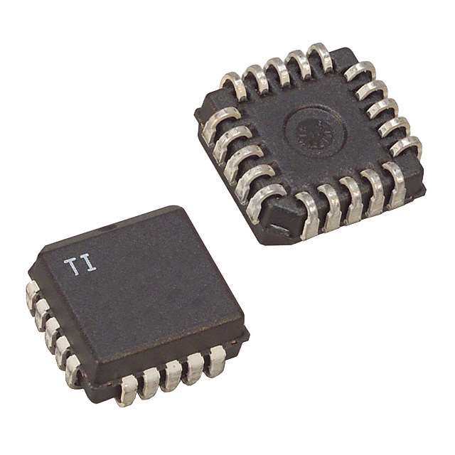
| 描述 | IC REG CTRLR BUCK PWM CM 32-QFN |
| 产品分类 | |
| 品牌 | Intersil |
| 数据手册 | |
| 产品图片 |
|
| 产品型号 | ISL9444CRZ-T7A |
| PWM类型 | 电流模式 |
| rohs | 无铅 / 符合限制有害物质指令(RoHS)规范要求 |
| 产品系列 | - |
| 倍增器 | 无 |
| 其它名称 | ISL9444CRZ-T7ATR |
| 分频器 | 无 |
| 包装 | 带卷 (TR) |
| 升压 | 无 |
| 占空比 | - |
| 反向 | 无 |
| 反激式 | 无 |
| 封装/外壳 | 40-VFQFN 裸露焊盘 |
| 工作温度 | 0°C ~ 85°C |
| 标准包装 | 250 |
| 电压-电源 | 4.5 V ~ 28 V |
| 输出数 | 3 |
| 降压 | 是 |
| 隔离式 | 无 |
| 频率-最大值 | 1.32MHz |


- 商务部:美国ITC正式对集成电路等产品启动337调查
- 曝三星4nm工艺存在良率问题 高通将骁龙8 Gen1或转产台积电
- 太阳诱电将投资9.5亿元在常州建新厂生产MLCC 预计2023年完工
- 英特尔发布欧洲新工厂建设计划 深化IDM 2.0 战略
- 台积电先进制程称霸业界 有大客户加持明年业绩稳了
- 达到5530亿美元!SIA预计今年全球半导体销售额将创下新高
- 英特尔拟将自动驾驶子公司Mobileye上市 估值或超500亿美元
- 三星加码芯片和SET,合并消费电子和移动部门,撤换高东真等 CEO
- 三星电子宣布重大人事变动 还合并消费电子和移动部门
- 海关总署:前11个月进口集成电路产品价值2.52万亿元 增长14.8%


PDF Datasheet 数据手册内容提取
DATASHEET ISL9444 FN7665 Triple, 180° Out-of-Phase, Synchronous Step-Down PWM Controller Rev 3.00 May 29, 2012 The ISL9444 is a triple-output synchronous buck controller that Features integrates three PWM controllers which are fully featured and designed to provide multi-rail power for use in products such as • Three Integrated Synchronous Buck PWM Controllers cable and satellite set-top boxes, VoIP gateways, cable modems, - Internal Bootstrap Diodes and other home connectivity products as well as a variety of - Independent Programmable Output Voltage industrial and general purpose applications. Each output is - Independent Power-Good Indicators, Soft-Starting and adjustable down to 0.7V. The PWMs are synchronized at 180° Tracking out-of-phase, thus reducing the input RMS current and ripple voltage. • Power Failure Monitor The ISL9444 offers independent power-good indicators, • Light Load Efficiency Enhancement programmable soft-start and tracking functions for ease of - Low Ripple Diode Emulation Mode with Pulse Skipping supply rail sequencing and integrated UV/OV/OC/OT • Supports Pre-Biased Output protections in a space conscious 5mmx5mm QFN package. • Programmable Frequency: 200kHz to 1200kHz Switching frequency can be set between 200kHz and 1200kHz • Adaptive Shoot-through Protection using a resistor. The ISL9444 can be synchronized to another ISL9444 to reduce any beat frequency. • Out-of-Phase Switching (0°/180°/0°) The ISL9444 utilizes internal loop compensation to keep • No External Current Sense Resistor minimum peripheral components for a compact design and a - Uses Lower MOSFET’s r DS(ON) low total solution cost. These devices are implemented with • Complete Protection current mode control with feed-forward to cover various - Overcurrent, Overvoltage, Over-Temperature applications even with fixed internal compensations. • Wide Input Voltage Range: 4.5V to 28V Related Literature • Pb-Free (RoHS Compliant) • Technical Brief TB389 “PCB Land Pattern Design and Applications Surface Mount Guidelines for QFN (MLFP) Packages” • VoX Gateway Devices • NAS/SAN Devices • ATX Power Supplies +12V + Q1 Q2 CIN1 CIN2 L2 2.2µH VOUT2 +3.3V, 6A 0.1µF 0.1µF + CO2 VOUT1 RESN2 R9 100µF +1.0V, 6A L1 RESN1 CB1 CB2 1.3kΩ 11.5kΩ 1.3kΩ 10C0OµF1+ 1.0µH +12V C1 VVISICNECN_15V LGATE1 PHASE1 BOOT1 UGATE1 PGND UGATE2 BOOT2 PHASE2 LGATE2 ISEFNB22 +12V 3.09kRΩ8 R2 4.7µF 62kΩ EXTBIAS UGATE3 PFI ISL9444 BOOT3 Q3 15.8kRΩ4 10kRΩ1 PEFNO2,3 PHASE3 0.C1µBF3 L3 3.3µH +V5.O0VU,T 63A 31.6kRΩ3 RT RFEBNT1/SS1 SGND OCSET1 OCSET2 OCSET2 MODE/SYNCCLKOUTPGOOD1,2,3TK/SS2,3 FB3 LGISAETNE33 R1.E3kSΩN3 R4 + C10O03µF 49.9kΩ CSS 10.7kΩ 10nF R5 R6 R7 100kΩ 200kΩ 200kΩ R3 1.74kΩ FIGURE 1. TYPICAL APPLICATION FN7665 Rev 3.00 Page 1 of 25 May 29, 2012
ISL9444 Ordering Information PART NUMBER PART TEMP. RANGE PACKAGE PKG. (Notes 1, 2, 3) MARKING (°C) (Pb-Free) DWG. # ISL9444IRZ ISL9444 IRZ -40 to +85 40 Ld 5x5 QFN L40.5X5B ISL9444CRZ ISL9444 CRZ -0 to +85 40 Ld 5x5 QFN L40.5X5B ISL9444EVAL1Z Evaluation Board NOTES: 1. Add “-T*” for tape and reel. Please refer to TB347 for details on reel specifications. 2. These Intersil Pb-free plastic packaged products employ special Pb-free material sets, molding compounds/die attach materials, and 100% matte tin plate plus anneal (e3 termination finish, which is RoHS compliant and compatible with both SnPb and Pb-free soldering operations). Intersil Pb-free products are MSL classified at Pb-free peak reflow temperatures that meet or exceed the Pb-free requirements of IPC/JEDEC J STD-020. 3. For Moisture Sensitivity Level (MSL), please see device information page for ISL9444. For more information on MSL please see techbrief TB363. Pin Configuration ISL9444 (40 LD 5x5 QFN) TOP VIEW 1 1 1 2 2 2 E 1 E E E E 2 E N1 AS OT AT AT AT AT OT AS N2 E H O G G G G O H E IS P B U L L U B P IS 40 39 38 37 36 35 34 33 32 31 PFO 1 30CLKOUT PFI 2 29PGND EXTBIAS 3 28LGATE3 VCC_5V 4 27UGATE3 VIN 5 26BOOT3 EN/SS1 6 25PHASE3 FB1 7 24ISEN3 OCSET1 8 23MODE/SYNC RT 9 22EN3 PGOOD1 10 21 TK/SS3 11 12 13 14 15 16 17 18 19 20 PGOOD2 PGOOD3 PG3_DLY EN2 SGND OCSET2 FB2 TK/SS2 OCSTET3 FB3 Pin Descriptions PIN NAME FUNCTION 1 PFO Output of the auxiliary power monitor. PFO goes high if the voltage on PFI is greater than 1.2V (typical). Otherwise the PFO outputs low. 2 PFI Input to the auxiliary power monitor. The internal threshold voltage is 1.2V (typical). 3 EXTBIAS Input from an optional external 5V bias supply. There is an internal switch from this pin to VCC_5V. This switch closes and supplies the IC power, bypassing the internal linear regulator, when voltage at EXTBIAS is higher than 4.7V (typ). Do not allow voltage at the EXTBIAS pin to exceed VIN at any time. Decouple this pin to ground with a small ceramic capacitor (0.1µF to 1µF) when it is in use, otherwise tie this pin to ground. Do not float this pin. 4 VCC_5V Output of the internal 5V linear regulator. This output supplies bias for the IC, the low side gate drivers, and the external boot circuitry for the high-side gate drivers. The VCC_5V pin must be always decoupled to power ground with a minimum of 4.7µF ceramic capacitor, placed very close to the pin. Do not allow the voltage at VCC_5V to exceed VIN at any time. FN7665 Rev 3.00 Page 2 of 25 May 29, 2012
ISL9444 Pin Descriptions (Continued) PIN NAME FUNCTION 5 VIN This pin should be tied to the input rail. It provides power to the internal linear drive circuitry and is also used by the feed-forward controller to adjust the amplitude of each PWM sawtooth. Decouple this pin with a small ceramic capacitor (0.1µF to 1µF) to ground. 6 EN/SS1 This pin provides an enable/disable function and soft-starting for PWM1 output. The output is disabled when the pin is pulled to GND. During start-up, a regulated 1.55µA soft-start current charges an external capacitor connected at this pin. When the voltage on the EN/SS1 pin reaches 1.3V, the PWM1 output becomes active. From 1.3V to 2.0V, the reference voltage of the PWM1 is clamped to the voltage at EN/SS1 minus 1.3V. The capacitance of the soft-start capacitors sets the soft-starting time and enable delay time. Setting the soft-starting time too short might create undesirable overshoot at the output during start-up. VCC_5V UVLO discharges the EN/SS1 via an internal MOSFET. 7 FB1 PWM1 feedback input. Connect FB1 to a resistive voltage divider from the output of PWM1 to GND to adjust the output voltage. 8 OCSET1 A resistor from this pin to ground adjusts the overcurrent threshold for PWM1. 9 RT A resistor from this pin to ground adjusts the switching frequency from 200kHz to 1.2MHz. The switching frequency of the PWM controller is determined by the resistor, R, T R = 23.361.5t –0.36k (EQ. 1) T SW where t is the switching period in µs. SW 10 PGOOD1 Open drain logic output used to indicate the status of the PWM1 output voltage. This pin is pulled down when the PWM1 output is not within ±11% of the nominal voltage. 11 PGOOD2 Open drain logic output used to indicate the status of the PWM2 output voltage. This pin is pulled down when the PWM2 output is not within ±11% of the nominal voltage. 12 PGOOD3 Open drain logic output used to indicate the status of the PWM3 output voltage. This pin is pulled down when the PWM3 output is not within ±11% of the nominal voltage. 13 PG3_DLY A capacitor connected between this pin and ground sets a delay between PWM3 output voltage reaching ±11% of regulation and PGOOD3 going high. There is no delay when PWM3 goes out of regulation and PGOOD3 is pulled low. 14 EN2 Enable/Disable input for PWM2. The output of PWM2 is enabled when this pin is pulled HIGH, and disabled when this pin is pulled LOW. PGOOD2 is pulled LOW 1µs after EN2 is pulled LOW. Do not leave this pin floating. 15 SGND This is the small-signal ground common to all 3 controllers. It is suggested to route this separately from the high current ground (PGND). SGND and PGND can be tied together if there is one solid ground plane with no noisy currents around the chip. All voltage levels are measured with respect to this pin. 16 OCSET2 A resistor from this pin to ground adjusts the overcurrent threshold for PWM2. 17 FB2 PWM2 feedback input. Connect FB2 to a resistive voltage divider from the output of PWM2 to GND to adjust the output voltage. 18 TK/SS2 Dual function pin. The reference voltage of PWM2 is clamped to the voltage at TK/SS2 during start-up. When this pin is used for tracking, another channel is configured as the master and the output voltage of the master channel is applied to this pin via a resistor divider. When used for soft-starting control, a soft-start capacitor is connected from this pin to GND. A regulated 1.55µA soft-starting current charges up the soft-start capacitor. Value of the soft-start capacitor sets the PWM2 output voltage ramp. 19 OCSET3 A resistor from this pin to ground adjusts the overcurrent threshold for PWM3. 20 FB3 PWM3 feedback input. Connect FB3 to a resistive voltage divider from the output of PWM3 to GND to adjust the output voltage. 21 TK/SS3 Dual function pin. The reference voltage of PWM3 is clamped to the voltage at TK/SS3 during start-up. When this pin is used for tracking, another channel is configured as the master and the output voltage of the master channel is applied to this pin via a resistor divider. When used for soft-starting control, a soft-start capacitor is connected from this pin to GND. A regulated 1.55µA soft-starting current charges up the soft-start capacitor. Value of the soft-start capacitor sets the PWM3 output voltage ramp. 22 EN3 Enable/Disable input for PWM3. The output of PWM3 is enabled when this pin is pulled HIGH, and disabled when this pin is pulled LOW. PGOOD3 is pulled LOW 1µs after EN3 is pulled LOW. Do not leave this pin floating. FN7665 Rev 3.00 Page 3 of 25 May 29, 2012
ISL9444 Pin Descriptions (Continued) PIN NAME FUNCTION 23 MODE/SYNC Dual function pin. Tie this pin to ground or VCC_5V for DEM or CCM operation mode selection. Connect this pin to ground to select Diode Emulation Mode with pulse skipping at light load. While connected to VCC_5V, the controllers operate in PWM Mode at light load. Connect this pin to CLKOUT of another ISL9444 or an external clock for synchronization. The controller operates in PWM at light load when synchronized with another ISL9444 or with an external clock. 24 ISEN3 Current signal input for PWM3. This pin is used to monitor the voltage drop across the lower MOSFET for current loop feedback and overcurrent protection. 25 PHASE3 Phase node connection for PWM3. This pin is connected to the junction of the upper MOSFET’s source, output filter inductor, and lower MOSFET’s drain. PHASE3 is the internal lower supply rail for the UGATE3. 26 BOOT3 Bootstrap pin to provide bias for PWM3 high-side driver. The positive terminal of the bootstrap capacitor connects to this pin. The bootstrap diodes are integrated to help reduce total cost and reduce layout complexity. 27 UGATE3 High-side MOSFET gate driver output for PWM3. 28 LGATE3 Low-side MOSFET gate driver output for PWM3. 29 PGND Power ground connection for all three PWM channels. This pin should be connected to the sources of the lower MOSFETs and the (-) terminals of the external input capacitors 30 CLKOUT Clock signal output. The frequency of the clock signal is two times of the ISL9444 switching frequency set by the resistor from RT to ground. 31 ISEN2 Current signal input for PWM2. This pin is used to monitor the voltage drop across the lower MOSFET for current loop feedback and overcurrent protection. 32 PHASE2 Phase node connection for PWM2. This pin is connected to the junction of the upper MOSFET’s source, output filter inductor, and lower MOSFET’s drain. PHASE2 is the internal lower supply rail for the UGATE2. 33 BOOT2 Bootstrap pin to provide bias for PWM2 high-side driver. The positive terminal of the bootstrap capacitor connects to this pin. The bootstrap diodes are integrated to help reduce total cost and reduce layout complexity. 34 UGATE2 High-side MOSFET gate driver output for PWM2. 35 LGATE2 Low-side MOSFET gate driver output for PWM2. 36 LGATE1 Low-side MOSFET gate driver output for PWM1. 37 UGATE1 High-side MOSFET gate driver output for PWM1. 38 BOOT1 Bootstrap pin to provide bias for PWM1 high-side driver. The positive terminal of the bootstrap capacitor connects to this pin. The bootstrap diodes are integrated to help reduce total cost and reduce layout complexity. 39 PHASE1 Phase node connection for PWM1. This pin is connected to the junction of the upper MOSFET’s source, output filter inductor, and lower MOSFET’s drain. PHASE1 is the internal lower supply rail for the UGATE1. 40 ISEN1 Current signal input for PWM1. This pin is used to monitor the voltage drop across the lower MOSFET for current loop feedback and overcurrent protection. - EPAD EPAD at ground potential. Solder it directly to GND plane for better thermal performance. FN7665 Rev 3.00 Page 4 of 25 May 29, 2012
MaFN Block Diagram ISL y7 9 29, 20665R UBGOAOTTE11 VCC_5V PGOOD1 PGOOD2 PGOOD3PG3_DLYVIN VCC_5V EXTBIAS VCC_5V UBGOAOTET22 444 1e 2v 3 PHASE1 PHASE2 .00 ADAPTIVE DEAD-TIME 2µA + ADAPTIVE DEAD-TIME VCC_5V V/I SAMPLE TIMING _ V/I SAMPLE TIMING VCC_5V LGATE1 SW THRES. LGATE2 PGND POR PGND PGND ENABLE BOOT3 PFI BIAS SUPPLIES EN/SS1 VCC_5V + UGATE3 _ REFERENCE EN2 PF REF FAULT LATCH EN3 PHASE3 PFO (see Note 6) ADAPTIVE DEAD-TIME V/I SAMPLE TIMING VCC_5V LGATE3 FB1 180kΩ 1000kΩ 15pF _ 180kΩ OCP PGND + 16kΩ _ FB3 + 0.7V REF ERROR AMP 1 _ PWM1 OC1OC2OC3 OV PWM3 + 0.7V REF TK/SS3 + EN/SS1 + 1.55µA FB1 FB2 FB3 ERROR AMP 3 EN3 EN/SS1 OC3 1.3V VIN VCC_5V MINIMUM SOFT-START ISEN3 ISEN1 _ CURRENT DUTY CYCLE RAMP GENERATOR OCSET3 SAMPLE + CURRENT CHANNEL 3 SAMPLE PWM CHANNEL PHASE CONTROL OCSET1 FB2 + PWM2 1.75V REFERENCE TK/SS2 - EN3 P OC1 a ge + SAME STATE FOR ISEN2 5 of 25 CHANNEL 1 ORVE2EQ CRULCIORUCERKDR ECTNOYT CL LFAAETSUCLHT DE/SYNC CLKOUT RT OC2 CHANNEL 2 OCSET2 O M SGND
ISL9444 Typical Application - ISL9444 +12V + CIN1 100µF C1 C2 1µF 4.7µF 3 5 4 C4 C3 EXTBIAS VIN VCC_5V 10µF 10µF 38 BOOT1 BOOT2 33 C5 C6 0.1µF 37 UGATE1 34 UGATE2 0.1µF VOUT1 39 PHASE1 PHASE2 32 VOUT2 +1.05V, 6A L1 R3 40 ISEN1 31 R4 L2 +3.3V, 6A ISEN2 CO1 1.0µH 1.3K 1.3k 1.5µH CO2 100µF 36 LGATE1 35 47µF LGATE2 Q2 IRF7907 Q1 R1 C7 IRF7907 C8 R5 15.8k 470pF 47pF 115k 7 FB1 FB2 17 R2 V VOUT1 +12V R6 31.6k R13 ISL9444 30.9k 100k 10 C10 PGOOD1 PGOOD1 BOOT3 26 10µF 14 PGOOD1 EN2 27 22 UGATE3 C11 EN3 0.1µF 25 PHASE3 VOUT3 R7 8 100k OCSET1 R10 L3 +1.8V, 6A 24 R8 16 ISEN3 100k OCSET2 1.1k 1.5µH CO3 1R009k 19 OCSET3 LGATE3 28 Q3IRF7907 47µF CSS1 10nF 6 R11 C12 EN/SS1 16.5k 1000pF VOUT2 20 V R14 FB3 25.5k 21 TK/SS3 VOUT1 C9 V R12 DNP R15 CSS2 10.5k 49.9k 10nF 18 R18 TK/SS2 100k 20 PGOOD3 PGOOD 23 19 MODE/SYNC PGOOD2 2 13 PFI PG3_DLY CDLY 1 PFO 9 47nF RT CLKOUT PGND SGND 30 29 15 4R9T.9k FN7665 Rev 3.00 Page 6 of 25 May 29, 2012
ISL9444 Typical Application - ISL9444 +19V C10 0.1µF + CIN3 + CIN2 + CIN1 150µF 150µF 150µF EXTBIAS C1 C2 0.1µF 4.7µF CIN5 CIN4 3 5 4 CIN7 CIN6 10µF 10µF EXTBIAS VIN VCC_5V 10µF 10µF 33 BOOT2 RJK0332DPB 38 BOOT1 C3 Q1 37 UGATE2 34 Q4 C4 0.22µF UGATE1 Q3 0.22µF RJK0332DPB 32 29 PHASE2 VOUT2 PHASE1 VOUT1 R5 L2 + 12.0V, 15A +5.0V, 18A L1 R4 40 ISEN2 31 C5+ C6+ 2.2µH 2.0k ISEN1 35 3.92k QR5JK0329DPB 2.2µH +1C870µF +18C08µF 330µF 330µF Q2 36 LGATE2 LGATE1 CFF2 RJK0329DPB 1000pF CFF1 R3 R2 4700pF R6 17 200 52.3k 10.7k R16 FB2 200 ISL9444 7 R1 FB1 3.24k +16V R7 1.74k +16V PGOOD2 11 PGOOD2 V 23 R14 MODE/SYNC 26 CIN9 CIN8 64.9k BOOT3 10µF 10µF 2 PFI C9 UGATE3 27 Q6 0.22µF R15 1 RJK0332DPB 10k PFO PFO PHASE3 25 VOUT3 R8 L3 +3.3V, 15A 14 24 EN2 ISEN3 18 3.92k Q7 1.5µH +C10 + C11 CSS2 TK/SS2 LGATE3 27 RJK0329DPB 330µF 330µF 47nF CFF3 R9 22pF 6 EN/SS1 11.5k PGOOD2 20 CSS1 FB3 47nF R10 22 EN3 PGOOD1 3.09k 10 PGOOD1 PGOOD1 VOUT1 13 V 20R01k1 8 OCSET1 PG3_DLY RPG 100k R12 16 200k OCSET2 PGOOD3 12 PGOOD R13 19 OCSET3 200k TK/SS3 21 30 CLKOUT CSS3 PGNDSGND RT 47nF 29 15 9 RT 118k VOUT1 can be connected to EXTBIAS for lower IC power dissipation and IC self-bias. External boot diode may be added for PWM2. Care must be taken to ensure VIN does not drop below EXTBIAS. FN7665 Rev 3.00 Page 7 of 25 May 29, 2012
ISL9444 Table of Contents Absolute Maximum Ratings . . . . . . . . . . . . . . . . . . . . . . . . . . . . . . . . . . . . . . . . . . . . . . . . . . . . . . . . . . 9 Thermal Information . . . . . . . . . . . . . . . . . . . . . . . . . . . . . . . . . . . . . . . . . . . . . . . . . . . . . . . . . . . . . . . 9 Recommended Operating Conditions. . . . . . . . . . . . . . . . . . . . . . . . . . . . . . . . . . . . . . . . . . . . . . . . . . . 9 Electrical Specifications . . . . . . . . . . . . . . . . . . . . . . . . . . . . . . . . . . . . . . . . . . . . . . . . . . . . . . . . . . . . . . . . . . . . . . . . . . . . . . . . . . . . . 9 Typical Performance Curves of ISL9444 . . . . . . . . . . . . . . . . . . . . . . . . . . . . . . . . . . . . . . . . . . . . . . . . . . . . . . . . . . . . . . . . . . . 12 Functional Description . . . . . . . . . . . . . . . . . . . . . . . . . . . . . . . . . . . . . . . . . . . . . . . . . . . . . . . . . . . . . . . . . . . . . . . . . . . . . . . . . . 16 General Description . . . . . . . . . . . . . . . . . . . . . . . . . . . . . . . . . . . . . . . . . . . . . . . . . . . . . . . . . . . . . . . . . . . . . . . . . . . . . . . . . . .16 Input Voltage Range. . . . . . . . . . . . . . . . . . . . . . . . . . . . . . . . . . . . . . . . . . . . . . . . . . . . . . . . . . . . . . . . . . . . . . . . . . . . . . . . . . .16 Internal 5V Linear Regulator (VCC_5V) and External VCC Bias Supply (EXTBIAS) . . . . . . . . . . . . . . . . . . . . . . . . . . . . . . . .16 Enable Signals and Soft-Start Operation. . . . . . . . . . . . . . . . . . . . . . . . . . . . . . . . . . . . . . . . . . . . . . . . . . . . . . . . . . . . . . . . . .16 Output Voltage Programming. . . . . . . . . . . . . . . . . . . . . . . . . . . . . . . . . . . . . . . . . . . . . . . . . . . . . . . . . . . . . . . . . . . . . . . . . . .16 Tracking Operation. . . . . . . . . . . . . . . . . . . . . . . . . . . . . . . . . . . . . . . . . . . . . . . . . . . . . . . . . . . . . . . . . . . . . . . . . . . . . . . . . . . .17 Light Load Efficiency Enhancement. . . . . . . . . . . . . . . . . . . . . . . . . . . . . . . . . . . . . . . . . . . . . . . . . . . . . . . . . . . . . . . . . . . . . .17 Pre-biased Power-up. . . . . . . . . . . . . . . . . . . . . . . . . . . . . . . . . . . . . . . . . . . . . . . . . . . . . . . . . . . . . . . . . . . . . . . . . . . . . . . . . . . . . . . . . . .17 Frequency Selection. . . . . . . . . . . . . . . . . . . . . . . . . . . . . . . . . . . . . . . . . . . . . . . . . . . . . . . . . . . . . . . . . . . . . . . . . . . . . . . . . . .17 Frequency Synchronization. . . . . . . . . . . . . . . . . . . . . . . . . . . . . . . . . . . . . . . . . . . . . . . . . . . . . . . . . . . . . . . . . . . . . . . . . . . . . . . . . . . . .17 Out-of-Phase Operation . . . . . . . . . . . . . . . . . . . . . . . . . . . . . . . . . . . . . . . . . . . . . . . . . . . . . . . . . . . . . . . . . . . . . . . . . . . . . . . . . . . . . . . .17 Power Failure Monitor . . . . . . . . . . . . . . . . . . . . . . . . . . . . . . . . . . . . . . . . . . . . . . . . . . . . . . . . . . . . . . . . . . . . . . . . . . . . . . . . .18 Gate Control Logic . . . . . . . . . . . . . . . . . . . . . . . . . . . . . . . . . . . . . . . . . . . . . . . . . . . . . . . . . . . . . . . . . . . . . . . . . . . . . . . . . . . .18 Gate Drivers. . . . . . . . . . . . . . . . . . . . . . . . . . . . . . . . . . . . . . . . . . . . . . . . . . . . . . . . . . . . . . . . . . . . . . . . . . . . . . . . . . . . . . . . . .18 Adaptive Dead Time. . . . . . . . . . . . . . . . . . . . . . . . . . . . . . . . . . . . . . . . . . . . . . . . . . . . . . . . . . . . . . . . . . . . . . . . . . . . . . . . . . .18 Internal Bootstrap Diode. . . . . . . . . . . . . . . . . . . . . . . . . . . . . . . . . . . . . . . . . . . . . . . . . . . . . . . . . . . . . . . . . . . . . . . . . . . . . . .18 Power-Good Indicators. . . . . . . . . . . . . . . . . . . . . . . . . . . . . . . . . . . . . . . . . . . . . . . . . . . . . . . . . . . . . . . . . . . . . . . . . . . . . . . . .19 Protection Circuits. . . . . . . . . . . . . . . . . . . . . . . . . . . . . . . . . . . . . . . . . . . . . . . . . . . . . . . . . . . . . . . . . . . . . . . . . . . . . . . . . . . . . . 19 Undervoltage Lockout . . . . . . . . . . . . . . . . . . . . . . . . . . . . . . . . . . . . . . . . . . . . . . . . . . . . . . . . . . . . . . . . . . . . . . . . . . . . . . . . .19 Overcurrent Protection. . . . . . . . . . . . . . . . . . . . . . . . . . . . . . . . . . . . . . . . . . . . . . . . . . . . . . . . . . . . . . . . . . . . . . . . . . . . . . . . .19 Overvoltage Protection . . . . . . . . . . . . . . . . . . . . . . . . . . . . . . . . . . . . . . . . . . . . . . . . . . . . . . . . . . . . . . . . . . . . . . . . . . . . . . . .19 Over-Temperature Protection . . . . . . . . . . . . . . . . . . . . . . . . . . . . . . . . . . . . . . . . . . . . . . . . . . . . . . . . . . . . . . . . . . . . . . . . . . .19 Feedback Loop Compensation . . . . . . . . . . . . . . . . . . . . . . . . . . . . . . . . . . . . . . . . . . . . . . . . . . . . . . . . . . . . . . . . . . . . . . . . . . . 19 Layout Guidelines . . . . . . . . . . . . . . . . . . . . . . . . . . . . . . . . . . . . . . . . . . . . . . . . . . . . . . . . . . . . . . . . . . . . . . . . . . . . . . . . . . . . . . 20 Layout Considerations. . . . . . . . . . . . . . . . . . . . . . . . . . . . . . . . . . . . . . . . . . . . . . . . . . . . . . . . . . . . . . . . . . . . . . . . . . . . . . . . .20 General PowerPAD Design Considerations. . . . . . . . . . . . . . . . . . . . . . . . . . . . . . . . . . . . . . . . . . . . . . . . . . . . . . . . . . . . . . . .21 Component Selection Guideline . . . . . . . . . . . . . . . . . . . . . . . . . . . . . . . . . . . . . . . . . . . . . . . . . . . . . . . . . . . . . . . . . . . . . . . . . . 21 MOSFET Considerations. . . . . . . . . . . . . . . . . . . . . . . . . . . . . . . . . . . . . . . . . . . . . . . . . . . . . . . . . . . . . . . . . . . . . . . . . . . . . . . .21 Output Inductor Selection . . . . . . . . . . . . . . . . . . . . . . . . . . . . . . . . . . . . . . . . . . . . . . . . . . . . . . . . . . . . . . . . . . . . . . . . . . . . . .21 Output Capacitor Selection. . . . . . . . . . . . . . . . . . . . . . . . . . . . . . . . . . . . . . . . . . . . . . . . . . . . . . . . . . . . . . . . . . . . . . . . . . . . .21 Input Capacitor Selection . . . . . . . . . . . . . . . . . . . . . . . . . . . . . . . . . . . . . . . . . . . . . . . . . . . . . . . . . . . . . . . . . . . . . . . . . . . . . .22 Revision History. . . . . . . . . . . . . . . . . . . . . . . . . . . . . . . . . . . . . . . . . . . . . . . . . . . . . . . . . . . . . . . . . . . . . . . . . . . . . . . . . . . . . . . . 23 Products . . . . . . . . . . . . . . . . . . . . . . . . . . . . . . . . . . . . . . . . . . . . . . . . . . . . . . . . . . . . . . . . . . . . . . . . . . . . . . . . . . . . . . . . . . . . . . 24 Package Outline Drawing. . . . . . . . . . . . . . . . . . . . . . . . . . . . . . . . . . . . . . . . . . . . . . . . . . . . . . . . . . . . . . . . . . . . . . . . . . . . . . . . . . . . 25 FN7665 Rev 3.00 Page 8 of 25 May 29, 2012
ISL9444 Absolute Maximum Ratings Thermal Information VCC_5V to GND. . . . . . . . . . . . . . . . . . . . . . . . . . . . . . . . . . . . . -0.3V to +6.2V Thermal Resistance (Typical) (°C/W) (°C/W) JA JC EXTBIAS to GND . . . . . . . . . . . . . . . . . . . . . . . . . . . . . -0.3V to VCC_5V+0.3V 40 Ld QFN Package (Notes 4, 5) . . . . . . . . 30 2.5 VIN to GND. . . . . . . . . . . . . . . . . . . . . . . . . . . . . . . . . . . . . . . . . .-0.3V to +30V Maximum Junction Temperature . . . . . . . . . . . . . . . . . . . .-55°C to +150°C BOOT1,2,3/UGATE1,2,3 to PHASE1,2,3 . . . . . . . . . -0.3V to VCC_5V+0.3V Maximum Operating Temperature. . . . . . . . . . . . . . . . . . . .-40°C to +85°C PHASE1,2,3 and Maximum Storage Temperature. . . . . . . . . . . . . . . . . . . . .-65°C to +150°C ISEN1, 2,3, to GND. . . . . . . . . . . -5V (<100ns, 10µJ)/-0.3V (DC) to +30V Pb-free reflow profile . . . . . . . . . . . . . . . . . . . . . . . . . . . . . . . . see link below EN/SS1, EN2, EN3, FB1, FB2, FB3, to GND . . . . . . -0.3V to VCC_5V+0.3V http://www.intersil.com/pbfree/Pb-FreeReflow.asp OCSET1, OCSET2, OCSET3, PG3_DLY, TKSS2, TKSS3, CLKOUT, LGATE1, LGATE2, LGATE3, to GND. . . . . . . . . . . . -0.3V to VCC_5V+0.3V Recommended Operating Conditions RT, MODE/SYNC to GND . . . . . . . . . . . . . . . . . . . . . . -0.3V to VCC_5V+0.3V PFI, PFO, PGOOD1, 2, 3, to GND. . . . . . . . . . . . . . . . -0.3V to VCC_5V+0.3V Temperature . . . . . . . . . . . . . . . . . . . . . . . . . . . . . . . . . . . . . .-40°C to +85°C VCC_5V Short Circuit to GND Duration. . . . . . . . . . . . . . . . . . . . . . . . . . . . .1s Supply Voltage . . . . . . . . . . . . . . . . . . . . . . . . . . . . . . . . . . . . . . . 4.5V to 28V ESD Rating Human Body Model (Tested per JESD22-A114F). . . . . . . . . . . . . .3000V Machine Model (Tested per JESD22-115-C) . . . . . . . . . . . . . . . . . . .200V Charge Device Model (Tested per JESD22-C110D) . . . . . . . . . . . .2000V Latch Up (Tested per JESD78C; Class II, Level A, +85°C) . . . . . . . . 100mA CAUTION: Do not operate at or near the maximum ratings listed for extended periods of time. Exposure to such conditions may adversely impact product reliability and result in failures not covered by warranty. NOTES: 4. is measured in free air with the component mounted on a high effective thermal conductivity test board with “direct attach” features. See Tech JA Brief TB379. 5. For , the “case temp” location is the center of the exposed metal pad on the package underside. JC Electrical Specifications Recommended operating conditions unless otherwise noted. Refer to Block Diagram on page5 and Typical Application Schematics on pages 6 and 7. V = 5.0V to 28V, or VCC_5V = 5V ±10%, C_VCC_5V = 4.7µF, T = -40°C to +85°C, Typical values are at IN A T =+25°C, unless otherwise specified. Boldface limits apply over the operating temperature range, -40°C to +85°C. A MIN MAX SYMBOL PARAMETER TEST CONDITIONS (Note 9) TYP (Note 9) UNITS V SUPPLY IN V Input Voltage Range 4.5 12.0 28.0 V IN V SUPPLY CURRENT IN I Shutdown Current (Note 7) EN/SS1 = EN2 = EN3 = 0 32 40 µA VINQ PGOODx are floating I Operating Current (Note 8) PGOOD1, PGOOD2, PGOOD3 are floating 5 6 mA VINOP VCC_5V SUPPLY (Note 6) V Operation Voltage V = 12V, I = 0mA 5.1 5.4 5.7 V CC IN L Internal LDO Output Voltage V = 4.5V, I = 30mA 4.05 4.35 V IN L Internal LDO Output Voltage V > 5.6V, I = 75mA 4.5 5.4 V IN L I Maximum Supply Current of Internal LDO V = 0V, V = 12V 150 250 mA VCC_MAX VCC_5V IN EXTBIAS SUPPLY (Note 6) V Switch Over Threshold Voltage, Rising EXTBIAS Voltage 4.5 4.7 4.9 V EXT_THR V Switch Over Threshold Voltage, Falling EXTBIAS Voltage 4.35 4.5 4.65 V EXT_THF R Internal Switch On Resistance V = 12V 0.5 1.0 EXT IN UNDERVOLTAGE LOCKOUT V Undervoltage Lockout, Rising VCC_5V Voltage 3.4 3.95 4.45 V UVLOTHR V Undervoltage Lockout, Falling VCC_5V Voltage 3.05 3.60 4.15 V UVLOTHF EN/SS1, EN2, EN3 THRESHOLD V EN/SS1 THRESHOLD 1.10 1.30 1.5 V ENSS_TH V EN2, EN3 Logic Threshold, Rising 1.40 1.7 2.00 V EN_THR V EN2, EN3 Logic Threshold, Falling 1.10 1.25 1.40 V EN_THF FN7665 Rev 3.00 Page 9 of 25 May 29, 2012
ISL9444 Electrical Specifications Recommended operating conditions unless otherwise noted. Refer to Block Diagram on page5 and Typical Application Schematics on pages 6 and 7. V = 5.0V to 28V, or VCC_5V = 5V ±10%, C_VCC_5V = 4.7µF, T = -40°C to +85°C, Typical values are at IN A T =+25°C, unless otherwise specified. Boldface limits apply over the operating temperature range, -40°C to +85°C. (Continued) A MIN MAX SYMBOL PARAMETER TEST CONDITIONS (Note 9) TYP (Note 9) UNITS SOFT-START CURRENT I EN/SS1, TK/SSx Soft-Start Charge Current VEN/SS1 = VTK/SSx = 0V 1.05 1.55 2.05 µA SS DEFAULT INTERNAL MINIMUM SOFT-STARTING t Default Internal Output Ramping Time 1.3 2.1 2.9 ms SS_MIN POWER-FAIL MONITOR V PFI Input Threshold Voltage, Rising 1.16 1.22 1.28 V PFI_REF V PFI Input Threshold Voltage, Falling 1.05 1.12 1.19 V PFI_FAL V PFO Output Voltage Low I_SINK = 1mA 0.3 V PFO_L V PFO Output Voltage High I_SOURCE = 1mA VCC_5V -0.3 V PFO_H POWER-GOOD MONITORS V PGOODx Upper Threshold, PWM 1, 2 and 3 105.5 111 115.5 % PGOV V PGOODx Lower Threshold, PWM 1, 2 and 3 85 89 94 % PGUV V PGOODx Low Level Voltage I_SINK = 2mA 0.3 V PGLOW I PGOODx Leakage Current PGOODx = 5V 1 150 nA PGLKG PGOOD Rise Time RPULLUP = 10k to 3.3V 0.05 µs PGOOD Fall Time RPULLUP = 10k to 3.3V 0.05 µs PGOOD1, PGOOD2 TIMING t VOUT Rising Threshold to PGOOD Rising 0.7 1.1 1.5 ms PGR t VOUT Falling Threshold to PGOOD Falling 40 75 110 µs PGF EN2, EN3 Falling Threshold to PGOOD Falling 1.2 1.7 µs PGOOD3 TIMING PG3_DLY Charge Current V = 1.2V 1.2 1.9 2.6 µA PG3_DLY PG3_DLY Threshold Voltage (Note 9) 1.16 1.195 1.23 V REFERENCE SECTION V Internal Reference Voltage 0.700 V REF Reference Voltage Accuracy T = 0°C to +85°C -1.0 +1.0 % A T = -40°C to +85°C -1.15 +1.0 % A V FB Voltage Accuracy T = -40°C to +85°C -1.5 +1.5 % FBx A I FB Bias Current (Note 9) 100 nA FBLKG PWM CONTROLLER ERROR AMPLIFIERS DC Gain (Note 9) 88 dB GBW Gain-BW Product (Note 9) 15 MHz SR Slew Rate (Note 9) 2.0 V/µs PWM REGULATOR t Minimum Off Time R = 169k 95 125 155 ns OFF_MIN T DV Peak-to-Peak Saw-tooth Amplitude (Note 9) V = 12V 1.2 V RAMP IN V = 5.0V 0.55 V IN Ramp Offset 1 V FN7665 Rev 3.00 Page 10 of 25 May 29, 2012
ISL9444 Electrical Specifications Recommended operating conditions unless otherwise noted. Refer to Block Diagram on page5 and Typical Application Schematics on pages 6 and 7. V = 5.0V to 28V, or VCC_5V = 5V ±10%, C_VCC_5V = 4.7µF, T = -40°C to +85°C, Typical values are at IN A T =+25°C, unless otherwise specified. Boldface limits apply over the operating temperature range, -40°C to +85°C. (Continued) A MIN MAX SYMBOL PARAMETER TEST CONDITIONS (Note 9) TYP (Note 9) UNITS SWITCHING FREQUENCY (Note 9) F Switching Frequency R = 20.5k 1080 1200 1320 kHz SW T Switching Frequency R = 169k 168 198 228 kHz T Switching Frequency R = 49.9k 540 600 660 kHz T V RT Voltage R = 49.9k 485 500 515 mV RT T CLOCK OUTPUT AND SYNCHRONIZATION V CLKOUT Output High ISOURCE = 1mA VCC_5V - 0.3 V CLKH V CLKOUT Output Low ISINK = 1mA 0.3 V CLKL F CLKOUT Frequency R = VCC_5V 1080 1200 1320 kHz CLK T F SYNC Synchronization Range R = 49.9k 1020 1380 kHz SYNC T LIGHT LOAD EFFICIENCY MODE V MODE/SYNC Threshold High 1.3 1.6 1.9 V MODETHH V MODE/SYNC Threshold Low 1.1 1.4 1.7 V MODETHL V Diode Emulation Phase Threshold (Note 11) V = 12V -3 mV CROSS IN PWM GATE DRIVER (Note 9) I Source Current 800 mA GSRC I Sink Current 2000 mA GSNK R Upper Drive Pull-Up VCC_5V = 5.0V 1.5 3 Ω UG_UP R Upper Drive Pull-Down VCC_5V = 5.0V 1.1 2.5 Ω UG_DN R Lower Drive Pull-Up VCC_5V = 5.0V 1.5 3 Ω LG_UP R Lower Drive Pull-Down VCC_5V = 5.0V 0.6 1.5 Ω LG_DN t Rise Time C = 1000pF 8 ns GR OUT t Fall Time C = 1000pF 10 ns GF OUT OVERVOLTAGE PROTECTION V OV Trip Point 114.5 118.5 123.5 % OVTH OVERCURRENT PROTECTION I Overcurrent Threshold (OCSET_) (Note 10) ROCSET = 55k 32 µA OCSET Full Scale Input Current (ISEN_) (Note 10) 15 µA V Overcurrent Set Voltage (OCSET_) 1.67 1.74 1.81 V OCSET OVER-TEMPERATURE (Note 9) T Over-Temperature Shutdown 150 °C OT-TH T Over-Temperature Hysteresis 15 °C OT-HYS NOTES: 6. In normal operation, where the device is supplied with voltage on the VIN pin, the VCC_5V pin provides a 5V output capable of 75mA (min). When the VCC_5V pin is connected to external 5V supply, the internal LDO regulator is disabled. The voltage at VCC_5V should not exceed the voltage at VIN at any time. (Refer to the“Pin Descriptions” on page2 for more details.) 7. This is the total shutdown current with V = 5.6V and 28V. IN 8. Operating current is the supply current consumed when the device is active but not switching. It does not include gate drive current. 9. Parameters with MIN and/or MAX limits are 100% tested at +25°C, unless otherwise specified. Temperature limits established by characterization and are not production tested. 10. Check Note 6 for VCC_5V and VIN configurations. 11. Threshold voltage at PHASE1, PHASE2 and PHASE3 pins for turning off the bottom MOSFET during DEM. FN7665 Rev 3.00 Page 11 of 25 May 29, 2012
ISL9444 Typical Performance Curves of ISL9444 Oscilloscope plots are taken using the ISL9444EVAL1Z Evaluation Board, V = 12V, VOUT1 = 1.05V, VOUT2 = 3.3V, VOUT3 = 1.8V unless otherwise noted. IN 33.0 5.3 µA) 32.5 mA) 5.1 VIN = 28V NT ( 32.0 NT ( E E RR RR 4.9 CU 31.5 CU N G W N 4.7 DO 31.0 ATI VIN = 4.5V T R U E H P 4.5 S 30.5 O 30.0 4.3 -40 -20 0 20 40 60 80 100 -40 -20 0 20 40 60 80 100 TEMPERATURE (°C) TEMPERATURE (°C) o FIGURE 2. SHUTDOWN CURRENT vs TEMPERATURE FIGURE 3. QUIESCENT CURRENT vs TEMPERATURE 6 2.0 CHANNEL 1/2 5 A) 1.6 AGE (V) 4 T PINRENT (µ 1.2 T RR CHANNEL 3 VCC_5V VOL 23 SOFT-STACHARGING CU 00..48 1 0 0 0 50 100 150 200 250 0 0.5 1.0 1.5 2.0 2.5 3.0 3.5 4.0 4.5 VCC_5V LOAD CURRENT (mA) SOFT-START PIN VOLTAGE (V) FIGURE 4. VCC_5V vs LOAD REGULATION FIGURE 5. SOFT-START PIN CHARGING CURRENT vs VOLTAGE ON SOFT-START PIN 120 %) CHANNEL 2/3 GE (100 PWM1 A T L O 80 V T CHANNEL 1 U PWM2 P T 60 U O D E 40 Z PWM3 LI A M 20 R O N TIME @ 1µs/DIV 0 0 0.5 1.0 1.5 2.0 2.5 3.0 3.5 4.0 4.5 SOFT-START PIN VOLTAGE (V) FIGURE 6. NORMALIZED OUTPUT VOLTAGE vs VOLTAGE ON FIGURE 7. PHASE NODE WAVEFORMS. ALL OUTPUT VOLTAGES SOFT-START PIN SET AT 1.05V FN7665 Rev 3.00 Page 12 of 25 May 29, 2012
ISL9444 Typical Performance Curves of ISL9444 Oscilloscope plots are taken using the ISL9444EVAL1Z Evaluation Board, V = 12V, VOUT1 = 1.05V, VOUT2 = 3.3V, VOUT3 = 1.8V unless otherwise noted. (Continued) IN 650 720 Hz) V) k 630 m QUENCY ( 610 OLTAGE ( 710 FRE E V 700 G 590 NC N E HI R C E 690 WIT 570 REF S 550 680 -40 -20 0 20 40 60 80 100 -40 -20 0 20 40 60 80 100 TEMPERATURE (°C) TEMPERATURE (°C) FIGURE 8. SWITCHING FREQUENCY vs TEMPERATURE (R = 49.9kΩ) FIGURE 9. REFERENCE VOLTAGE vs TEMPERATURE T 100 1.055 1.000 EFFICIENCY DEM (%) 90 V) CIENCY (%) 56780000 VOUT1 (V) 11..004571 PUT VOLTAGE ( CURRENT (A) 0.100 CCM EFFI 3400 1.043 1 OUT NPUT 0.010 M I 20 1.039 W DEM EFFICIENCY CCM (%) P 10 0 1.035 0.001 0.01 0.1 1 10 0.01 0.1 1 10 LOAD CURRENT (A) LOAD CURRENT (A) FIGURE 10. PWM1 EFFICIENCY AND LOAD REGULATION FIGURE 11. PWM1 INPUT CURRENT COMPARISON WITH MODE=CCM/DEM 100 3.300 10.000 EFFICIENCY DEM (%) 90 V) %) 7800 VOUT2 (V) 3.296 TAGE ( T (A) 1.000 CY ( 60 3.292 VOL REN CCM EN 50 UT UR 0.100 CI P C EFFI 3400 EFFICIENCY CCM (%) 3.288 M2 OUT INPUT 0.010 DEM 20 3.284 W P 10 0 3.280 0.001 0.01 0.1 1 10 0.01 0.1 1 10 LOAD CURRENT (A) LOAD CURRENT (A) FIGURE 12. PWM2 EFFICIENCY AND LOAD REGULATION FIGURE 13. PWM2 INPUT CURRENT COMPARISON WITH MODE=CCM/DEM FN7665 Rev 3.00 Page 13 of 25 May 29, 2012
ISL9444 Typical Performance Curves of ISL9444 Oscilloscope plots are taken using the ISL9444EVAL1Z Evaluation Board, V = 12V, VOUT1 = 1.05V, VOUT2 = 3.3V, VOUT3 = 1.8V unless otherwise noted. (Continued) IN 100 1.800 10.000 90 V) 80 EFFICIENCY DEM (%) VOUT3 (V) 1.798 GE ( A) 1.000 CY (%) 6700 1.796 VOLTA RENT ( CCM EFFICIEN 345000 EFFICIENCY CCM (%) 1.794 M3 OUTPUT INPUT CUR 00..011000 DEM 20 1.792 W P 10 0 1.790 0.001 0.01 0.1 1 10 0.01 0.1 1 10 LOAD CURRENT (A) LOAD CURRENT (A) FIGURE 14. PWM3 EFFICIENCY AND LOAD REGULATION FIGURE 15. PWM3 INPUT CURRENT COMPARISON WITH MODE=CCM/DEM ENSS1 @ 2V/DIV ENSS1 @ 2V/DIV VOUT1 @ 1V/DIV VOUT1 @ 1V/DIV PGOOD1 @ 5V/DIV PGOOD1 @ 5V/DIV INDUCTOR CURRENT @ 1A/DIV INDUCTOR CURRENT @ 1A/DIV TIME @ 5ms/DIV TIME @ 5ms/DIV FIGURE 16. PWM1 START-UP. MODE = CCM, LOAD = 0A FIGURE 17. PWM1 START-UP. MODE = DEM, LOAD = 0A TIME @ 5ms/DIV TKSS2 @ 2V/DIV TKSS2 @ 2V/DIV VOUT2 @ 2V/DIV VOUT2 @ 2V/DIV PGOOD2 @ 5V/DIV PGOOD2 @ 5V/DIV INDUCTOR CURRENT @ 2A/DIV INDUCTOR CURRENT @ 1A/DIV TIME @ 5ms/DIV FIGURE 18. PWM2 START-UP. MODE = CCM, LOAD = 0A FIGURE 19. PWM2 START-UP. MODE = DEM, LOAD = 0A FN7665 Rev 3.00 Page 14 of 25 May 29, 2012
ISL9444 Typical Performance Curves of ISL9444 Oscilloscope plots are taken using the ISL9444EVAL1Z Evaluation Board, V = 12V, VOUT1 = 1.05V, VOUT2 = 3.3V, VOUT3 = 1.8V unless otherwise noted. (Continued) IN TIME @ 5ms/DIV TKSS3 @ 2V/DIV TKSS3 @ 2V/DIV VOUT3 @ 1V/DIV VOUT3 @ 1V/DIV PGOOD3 @ 5V/DIV PGOOD3 @ 5V/DIV INDUCTOR CURRENT @ 2A/DIV INDUCTOR CURRENT @ 2A/DIV TIME @ 5ms/DIV FIGURE 20. PWM3 START-UP. MODE = CCM, LOAD = 0A FIGURE 21. PWM3 START-UP. MODE = DEM, LOAD = 0A VOUT1 @ 20mV/DIV. LOAD = 0mA VOUT1 @ 20mV/DIV. LOAD = 0mA TIME @ 2ms/DIV TIME @ 2µs/DIV VOUT1 @ 20mV/DIV. LOAD = 100mA VOUT1 @ 20mV/DIV. LOAD = 100mA TIME @ 2µs/DIV TIME @ 2µs/DIV VOUT1 @ 20mV/DIV. LOAD = 1000mA VOUT1 @ 20mV/DIV. LOAD = 1000mA TIME @ 2µs/DIV TIME @ 2µs/DIV FIGURE 22. PWM1 OUTPUT RIPPLE, MODE = 0V (DEM) FIGURE 23. PWM1 OUTPUT RIPPLE, MODE = 5V (CCM) VOUT1 @ 100mV/DIV VOUT1 @ 1V/DIV VOUT2 @ 100mV/DIV ENSS1 @ 5V/DIV VOUT3 @ 100mV/DIV OUTPUT CURRENT @ 10A/DIV 4A 2A 2A PGOOD1 @ 5V/DIV TIME @ 20µs/DIV TIME @ 50ms/DIV FIGURE 24. PWM LOAD TRANSIENT RESPONSE FIGURE 25. PWM1 OCP RESPONSE. OUTPUT SHORT-CIRCUITED TO GROUND AND RELEASED. FN7665 Rev 3.00 Page 15 of 25 May 29, 2012
ISL9444 Functional Description When large MOSFETs are used, an external 5V bias voltage can be applied to EXTBIAS pin to alleviate excessive power General Description dissipation. Voltage at the EXTBIAS pin must always be lower than the voltage at the VIN pin to prevent biasing of the power The ISL9444 integrates control circuits for three synchronous stage through EXTBIAS and VCC_5V. An external UVLO circuit buck converters. The three synchronous bucks operate might be necessary to guarantee smooth soft-starting. out-of-phase to substantially reduce the input ripple and thus reduce the input filter requirements. The internal LDO has an overcurrent limit of typically 150mA. For better efficiency, connect VCC_5V to VIN for 5V ±10% input Each part has 3 independent enable/disable control lines applications. (EN/SS1, EN2 and EN3), which provide flexible power-up sequencing. The soft-start time is programmable individually by Enable Signals and Soft-Start Operation adjusting the soft-start capacitors connected from EN/SS1, Typical applications for the ISL9444 use programmable analog TK/SS2 and TK/SS3, respectively. soft-start or the TK/SSx pins for tracking. The soft-start time can The valley current mode control scheme with input voltage be set by the value of the soft-start capacitors connected from feed-forward ramp simplifies loop compensation and provides the EN/SS1 for PWM1 to ground and from TK/SSx pins to ground excellent rejection to input voltage variation. for PWM2 and PWM3. Inrush current during start-up can be alleviated by adjusting the soft-starting time. Input Voltage Range After the VCC_5V pin reaches the UVLO threshold, the ISL9444 The ISL9444 is designed to operate from input supplies ranging PWM1 soft-start circuitry becomes active. The internal 1.55µA from 4.5V to 28V. charge current begins charging up the soft-start capacitor The input voltage range can be effectively limited by the connected from the EN/SS1 pin to GND. The PWM1 output available minimum PWM off time. remains inactive until voltage on the EN/SS1 pin reaches 1.3V. As the voltage on the EN/SS1 pin rises from 1.3V to 2V, the V = ------------V----O---U----T----+-----V---d----1-------------+V –V (EQ. 2) PWM1 reference voltage is clamped to the voltage on the INmin 1–tOFFminFSW d2 d1 EN/SS1 pin minus 1.3V. PWM1 output voltage thus rises from 0V to regulation as EN/SS1 rises from 1.3V to 2V. Charging of the where, soft-start capacitor continues until the voltage on the EN/SS1 pin V = sum of the parasitic voltage drops in the inductor discharge d1 reaches 3.5V. path, including the lower FET, inductor and PC board. V = sum of the voltage drops in the charging path, including the Power sequencing can be achieved by using the PGOODx and d2 upper FET, inductor and PC board resistances. ENx pins. When the ENx pin is pulled high, the internal 1.55µA charge current begins charging up the soft-start capacitor The maximum input voltage and minimum output voltage is connected from the TK/SSx pin to GND. The respective reference limited by the minimum on-time (t ). ON(min) voltage is clamped to the voltage on the TK/SSx pin. Thus, PWM2 V and PWM3 output voltages ramp from 0V to regulation as VINmaxt------------------O----U---T-----F----------- (EQ. 3) voltage on TK/SS2 and TK/SS3 goes up from 0V to 0.7V. ONmin SW Charging of the soft-start capacitors continues until the voltage Where t = 100ns. on the TK/SSx reaches 3.5V. ON(min) The typical soft-start time is set according to Equation 4: Internal 5V Linear Regulator (VCC_5V) and External VCC Bias Supply (EXTBIAS) t = 0.7V----C----S---S----x----- (EQ. 4) SSx 1.55A All ISL9444 functions can be internally powered from an on-chip, low dropout 5V regulator or an external 5V bias voltage via the For PWM2 and PWM3, when the soft-starting time set by EXTBIAS pin. Bypass the linear regulator’s output (VCC_5V) with a external C or tracking is less than 2ms, an internal soft-start SS 4.7µF capacitor to the power ground. The ISL9444 also employs circuit of 2ms takes over the soft-start. There is no internal an undervoltage lockout circuit which disables all regulators soft-start for PWM1. when VCC_5V falls below 3.6V. PGOODx will toggle to high when the corresponding output is up The internal LDO can source over 75mA to supply the IC, power and in regulation. the low side gate drivers and charge the boot capacitors. When driving large FETs at high switching frequency, little or no Pulling the ENx low disables the corresponding PWM channel. regulator current may be available for external loads. The TK/SSx pin will also be discharged to GND by internal MOSFETs. For example, a single large FET with 15nC total gate charge requires 15nC x 300kHz = 4.5mA (15nC x 600kHz = 9mA). Also, Output Voltage Programming at higher input voltages with larger FETs, the power dissipation The ISL9444 provides a precision internal reference voltage to across the internal 5V will increase. Excessive dissipation across set the output voltage. Based on this internal reference, the this regulator must be avoided to prevent junction temperature output voltage can thus be set from 0.7V up to a level rise. Thermal protection may be triggered if die temperature determined by the input voltage, the maximum duty cycle, and increases above +150°C due to excessive power dissipation. the conversion efficiency of the circuit. FN7665 Rev 3.00 Page 16 of 25 May 29, 2012
ISL9444 A resistive divider from the output to ground sets the output capacitance. The switching frequency of the ISL9444 is set by a voltage of any PWM channel. The center point of the divider shall resistor connected from the RT pin to GND according to be connected to the FBx pin. The output voltage value is Equation1. determined by Equation 5. See Equation 1 in “Pin Descriptions” on page2 for selecting R. T The frequency setting curve shown in Figure 26 assists in VOUTx = 0.7VR-----1---R--+--2---R----2--- (EQ. 5) selecting the correct value for RT. Where R1 is the top resistor of the feedback divider network and 1250 R2 is the bottom resistor connected from FBx to ground. Tracking Operation 1000 The PWM2 and PWM3 of the ISL9444 can be independently set z) H up to track the output of another PWM or an external supply. In Y (k 750 the following discussion, we refer to the voltage rail to be tracked C N as the master rail while we refer to the voltage rail that follows E U the master as the slave rail. To implement tracking, an additional Q 500 E R resistive divider is connected between the master rail and F ground. The center point of the divider shall be connected to the 250 TK/SSx pin of the slave PWM. The resistive divider ratio sets the ramping ratio between the two voltage rails. To implement coincident tracking, set the tracking resistive divider ratio exactly 0 the same as the slave rail output resistive divider given by 0 20 40 60 80 100 120 140 160 180 Equation 5. Make sure that the voltage at TK/SSx is greater than RT (kΩ) 0.7V when the master rail reaches regulation. FIGURE 26. R vs SWITCHING FREQUENCY T To minimize the impact of the 1.55µA soft-start current on the tracking function, it is recommended to use resistors of less than Frequency Synchronization 10kfor the tracking resistive dividers. The MODE/SYNC pin may be used to synchronize two or more When overcurrent protection (OCP) is triggered for the slave PWM ISL9444 or ISL9443 controllers. When the MODE/SYNC pin is channel, the internal minimum soft-start circuit determines the connected to the CLKOUT pin of another ISL9444, the two OCP soft-start hiccup. controllers operate in synchronization. Light Load Efficiency Enhancement When the MODE/SYNC pin is connected to an external clock, the ISL9444 will synchronize to this external clock at half of the clock When MODE/SYNC is tied to GND, the ISL9444 operates in high frequency. For proper operation, frequency setting resistor, R , efficiency diode emulation mode and pulse skipping mode in T should be set according to Equation 1 in “Pin Descriptions” on light load condition. The inductor current is not allowed to reverse page2. (discontinuous operation). At very light loads, the converter goes into diode emulation and triggers the pulse skipping function. When frequency synchronization is in action, the controllers will Here, the upper MOSFET remains off until the output voltage enter forced continuous current mode, CCM at light load. drops to the point the error amplifier output goes above the pulse Out-of-Phase Operation skipping mode threshold. The minimum t in the pulse skipping mode is 80ns; please To reduce input ripple current, the three PWM channels operate ON select frequency so that the PWM t is greater than 80ns at 180° out-of-phase. This reduces the input capacitor ripple current ON maximum VIN at no load. requirements, reduces power supply-induced noise, and improves EMI. This effectively helps to lower component cost, save board Pre-biased Power-up space and reduce EMI. The ISL9444 has the ability to soft-start with a pre-biased output. Triple PWMs traditionally operate in-phase and turn on all three The output voltage would not be yanked down during pre-biased upper FETs at the same time. The input capacitor must then support start-up. The PWM is not active until the soft-start ramp reaches the instantaneous current requirements of the three switching the output voltage times the resistive divider ratio. regulators simultaneously, resulting in increased ripple voltage and current. The higher RMS ripple current lowers the efficiency due to Overvoltage protection is alive during soft-starting. the power loss associated with the ESR of the input capacitor. This Frequency Selection typically requires more low-ESR capacitors in parallel to minimize the input voltage ripple and ESR-related losses, or to meet the Switching frequency selection is a trade-off between efficiency required ripple current specification. and component size. Low switching frequency improves efficiency by reducing MOSFET switching loss. To meet output With synchronized out-of-phase operation, the high-side ripple and load transient requirements, operation at a low MOSFETs turn off 180° out-of-phase. The instantaneous input switching frequency would require larger inductance and output current peaks of both regulators no longer overlap, resulting in FN7665 Rev 3.00 Page 17 of 25 May 29, 2012
ISL9444 reduced RMS ripple current and input voltage ripple. This OPTIONAL reduces the required input capacitor ripple current rating, EXTERNAL allowing fewer or less expensive capacitors, and reducing the SCHOTTKY VIN VCC_5V shielding requirements for EMI. The typical operating curves show the synchronized 180° out-of-phase operation. Power Failure Monitor BOOT RBOOT The ISL9444 has a Power-Failure Monitor that helps to monitor UGATE CB an additional critical voltage on the Power-Fail Input (PFI) pin. For example, the PFI pin could be used to provide an early power-fail PHASE warning, detect a low-battery condition, or simply monitor a power supply. An external resistor divider network is needed to provide monitoring of voltages greater than 1.22V. The threshold voltage is set according to Equation 6 (see Typical Application on ISL9444 page7). FIGURE 27. UPPER GATE DRIVER CIRCUIT R14+R15 VPFITH = 1.22V----------------------------- (EQ. 6) R15 Adaptive Dead Time PFO goes low whenever the PFI pin voltage is less than the 1.22V The ISL9444 incorporates an adaptive dead time algorithm on threshold voltage. the synchronous buck PWM controllers that optimizes operation with varying MOSFET conditions. This algorithm provides Gate Control Logic approximately 16ns of dead time between switching the upper The gate control logic translates generated PWM signals into gate and lower MOSFET’s. This dead time is adaptive and allows drive signals providing amplification, level shifting and operation with different MOSFET’s without having to externally shoot-through protection. The gate drivers have circuitry that helps adjust the dead time using a resistor or capacitor. During turn-off optimize the IC performance over a wide range of operational of the lower MOSFET, the LGATE voltage is monitored until it conditions. As MOSFET switching times can vary dramatically from reaches a threshold of 1V, at which time the UGATE is released to type to type and with input voltage, the gate control logic provides rise. Adaptive dead time circuitry monitors the upper MOSFET adaptive dead time by monitoring real gate waveforms of both the gate voltage during UGATE turn-off. Once the upper MOSFET upper and the lower MOSFETs. Shoot-through control logic provides gate-to-source voltage has dropped below a threshold of 1V, the a 16ns dead-time to ensure that both the upper and lower MOSFETs LGATE is allowed to rise. It is recommended to not use a resistor will not turn on simultaneously causing a shoot-through condition. between UGATE and LGATE and the respective MOSFET gates as it may interfere with the dead time circuitry. Gate Drivers Internal Bootstrap Diode The low-side gate drivers are supplied from VCC_5V and provide a peak sink current of 2A and source current of 800mA for each The ISL9444 has integrated bootstrap diodes to help reduce total PWM channel. The high-side gate drivers are also capable of cost and reduce layout complexity. Simply adding an external delivering the same currents as the low-side gate drivers. capacitor across the BOOT and PHASE pins completes the Gate-drive voltage for the upper N-Channel MOSFETs are bootstrap circuit. The bootstrap capacitor can be chosen from generated by flying capacitor boot circuits. A boot capacitor Equation 7. connected from the BOOT pin to the PHASE node provides power Q to the high-side MOSFET driver. To limit the peak current in the IC, C -------G---A----T---E---- (EQ. 7) an external resistor may be placed between the BOOT pin and the BOOT VBOOT boot capacitor. This small series resistor also damps any oscillations caused by the resonant tank of the parasitic Where Q is the amount of gate charge required to fully GATE inductances in the traces of the board and the FET’s input charge the gate of the upper MOSFET. The V term is defined BOOT capacitance. as the allowable droop in the rail of the upper drive. At start-up, the low-side MOSFET turns on first and forces PHASE As an example, suppose an upper MOSFET has a gate charge to ground in order to charge the BOOT capacitor to 5V. After the (QGATE) of 25nC at 5V and also assume the droop in the drive low-side MOSFET turns off, the high-side MOSFET is turned on by voltage over a PWM cycle is 200mV. One will find that a closing an internal switch between BOOT and UGATE. This bootstrap capacitance of at least 0.125µF is required. The next provides the necessary gate-to-source voltage to turn on the larger standard value capacitance of 0.22µF should be used. A upper MOSFET, an action that boosts the 5V gate drive signal good quality ceramic capacitor is recommended. above VIN. The current required to drive the upper MOSFET is drawn from the internal 5V regulator. The internal bootstrap Schottky diodes have a resistance of 1.5Ω (typ) at 800mA. Combined with the resistance RBOOT, this could For optimal EMI performance or reducing phase node ringing, a lead to the boot capacitor charging insufficiently in cases where small resistor might be placed between the BOOTx pins to the the bottom MOSFET is turned on for a very short time. If such positive terminal of the bootstrap capacitors. circumstances are expected, an additional external Schottky FN7665 Rev 3.00 Page 18 of 25 May 29, 2012
ISL9444 diode may be added from VCC_5V to the positive of the boot Because of the nature of this current sensing technique, and to capacitor. RBOOT may still be necessary to lower EMI due to fast accommodate a wide range of r variations, the value of the DS(ON) turn-on of the upper MOSFET. overcurrent threshold should represent an overload current about 150% to 180% of the maximum operating current. If more Power-Good Indicators accurate current protection is desired, place a current sense The three independent Power-good pins can be used to monitor resistor in series with the lower MOSFET source. the status of the output voltages. PGOODx will be true (open When OCP is triggered, the EN/SS1 or TK/SSx pins are pulled to drain) when the corresponding FBx pin is within ±11% of the ground by an internal MOSFET. For PWM rails configured to track reference voltage. another voltage rail, the TK/SSx pin rises up much faster than the internal minimum soft-start ramp. The voltage reference will Additionally, a capacitor from the PG3_DLY pin to the ground sets then be clamped to the internal minimum soft-start ramp. Thus a delay time for the PGOOD3 signal. After FB3 pin enters ±11% of the reference range, a 1.9µA current begins charging the CDLY smooth soft-start hiccup is achieved even with tracking function. capacitor. When the PG3_DLY voltage reaches 1.2V PGOOD3 Overvoltage Protection goes HIGH. All switching controllers within the ISL9444 have fixed The typical delay time is set according to Equation 8: overvoltage set points. The overvoltage set point is set at 118% C of the nominal output voltage, the output voltage set by the tDLY = 1.2V-1---.-9-D----L---YA--- (EQ. 8) feedback resistors. In the case of an overvoltage event, the IC will attempt to bring the output voltage back into regulation by There is no extra delay when the PGOOD3 pin is pulled LOW. keeping the upper MOSFET turned off and modulating the lower MOSFET for 2 consecutive PWM cycles. If the overvoltage Protection Circuits condition has not been corrected in 2 cycles and the output voltage is above 118% of the nominal output voltage, the The converter outputs are monitored and protected against ISL9444 will turn off both the upper MOSFET and the lower overload, short circuit and undervoltage conditions. MOSFET. The ISL9444 will enter hiccup mode until the output voltage returns to 110% of the nominal output voltage. Undervoltage Lockout Over-Temperature Protection The ISL9444 includes UVLO protection which keeps the device in a reset condition until a proper operating voltage is applied. It The IC incorporates an over-temperature protection circuit that also shuts down the ISL9444 if the operating voltage drops shuts the IC down when a die temperature of +150°C is below a pre-defined value. All controllers are disabled when UVLO reached. Normal operation resumes when the die temperatures is asserted. When UVLO is asserted, PGOOD1, PGOOD2 and drops below +130°C through the initiation of a full soft-start PGOOD3 are valid and will be de-asserted. cycle. When all three channels are disabled, thermal protection is inactive. This helps achieve a very low shutdown current of Overcurrent Protection 33µA. All the PWM controllers use the lower MOSFET's on-resistance, Feedback Loop Compensation r , to monitor the current in the converter. The sensed DS(ON) voltage drop is compared with a threshold set by a resistor To reduce the number of external components and to simplify the connected from the OCSETx pin to ground. process of determining compensation components, all PWM R = -----------7---------R----C---S------------ (EQ. 9) controllers have internally compensated error amplifiers. To OCSET I r make internal compensation possible, several design measures OC DSON were taken. Where I is the desired overcurrent protection threshold, and OC Firstly, the ramp signal applied to the PWM comparator is R is a value of the current sense resistor connected to the CS proportional to the input voltage provided at the VIN pin. This ISENx pin. keeps the modulator gain constant with varying input voltages. If an overcurrent is detected, the upper MOSFET remains off and Secondly, the load current proportional signal is derived from the the lower MOSFET remains on until the next cycle. As a result, the voltage drop across the lower MOSFET during the PWM time converter will skip a pulse. When the overload condition is interval and is subtracted from the amplified error signal on the removed, the converter will resume normal operation. comparator input. This creates an internal current control loop. The resistor connected to the ISEN pin sets the gain in the current If an overcurrent is detected for 2 consecutive clock cycles, the IC feedback loop. The following expression estimates the required enters a hiccup mode by turning off the gate drivers and entering value of the current sense resistor depending on the maximum soft-start. The IC will cycle 5 times through soft-start before trying to operating load current and the value of the MOSFET’s r . restart. The IC will continue to cycle through soft-start until the DS(ON) overcurrent condition is removed. Hiccup mode is active during I r R -----M----A----X----------D----S------O----N------- (EQ. 10) soft-start so care must be taken to ensure that the peak inductor CS 30A current does not exceed the overcurrent threshold during soft-start. Choosing R to provide 30µA of current to the current sample CS and hold circuitry is recommended but values down to 2µA and FN7665 Rev 3.00 Page 19 of 25 May 29, 2012
ISL9444 up to 100µA can be used. A higher sampling current will help to Layout Guidelines stabilize the loop. Careful attention to layout requirements is necessary for Due to the current loop feedback, the modulator has a single pole successful implementation of an ISL9444 based DC/DC response with -20dB slope at a frequency determined by the load. converter. The ISL9444 switches at a very high frequency and FPO = 2------------R--1----------C------ (EQ. 11) therefore the switching times are very short. At these switching O O frequencies, even the shortest trace has significant impedance. Also, the peak gate drive current rises significantly in an Where RO is load resistance and CO is load capacitance. For this extremely short time. Transition speed of the current from one type of modulator, a Type 2 compensation circuit is usually device to another causes voltage spikes across the sufficient. interconnecting impedances and parasitic circuit elements. These voltage spikes can degrade efficiency, generate EMI, Figure 28 shows a Type 2 amplifier and its response, along with increase device overvoltage stress and ringing. Careful the responses of the current mode modulator and the converter. component selection and proper PC board layout minimizes the The Type 2 amplifier, in addition to the pole at origin, has a magnitude of these voltage spikes. zero-pole pair that causes a flat gain region at frequencies between the zero and the pole. There are three sets of critical components in a DC/DC converter using the ISL9444: The controller, the switching power 1 F = ------------------------------ = 10kHz components and the small signal components. The switching Z 2R C (EQ. 12) 2 1 power components are the most critical from a layout point of view because they switch a large amount of energy so they tend to generate a large amount of noise. The critical small signal 1 FP = 2------------R------------C------ = 600kHz (EQ. 13) components are those connected to sensitive nodes or those 1 2 supplying critical bias currents. A multi-layer printed circuit board Zero frequency, amplifier high-frequency gain and modulator is recommended. gain are chosen to satisfy most typical applications. The Layout Considerations crossover frequency will appear at the point where the modulator attenuation equals the amplifier high frequency gain. The only 1. The input capacitors, upper FET, lower FET, inductor and task that the system designer has to complete is to specify the output capacitor should be placed first. Isolate these power output filter capacitors to position the load main pole components on the topside of the board with their ground somewhere within one decade lower than the amplifier zero terminals adjacent to one another. Place the input high frequency. With this type of compensation, plenty of phase frequency decoupling ceramic capacitors very close to the margin is easily achieved due to zero-pole pair phase ‘boost’. MOSFETs. 2. Use separate ground planes for power ground and small C2 signal ground. Connect the SGND and PGND together close to R2 C1 the IC. Do not connect them together anywhere else. CONVERTER R1 3. The loop formed by the input capacitor, the top FET and the bottom FET must be kept as small as possible. EA TYPE 2 EA 4. Ensure the current paths from the input capacitor to the MOSFET, to the output inductor and output capacitor are as GM = 17.5dB short as possible with maximum allowable trace widths. MODULATOR GEA = 18dB 5. Place the PWM controller IC close to the lower FET. The LGATE FZ FP connection should be short and wide. The IC can be best FPO FC pcularcreendt so vine rt ah iqs uaireeta g.round area. Avoid switching ground loop 6. Place VCC_5V bypass capacitor very close to VCC_5V pin of the IC and connect its ground to the PGND plane. 7. Place the gate drive components - optional BOOT diode and FIGURE 28. FEEDBACK LOOP COMPENSATION BOOT capacitors - together near controller IC. Conditional stability may occur only when the main load pole is 8. The output capacitors should be placed as close to the load as positioned too much to the left side on the frequency axis due to possible. Use short wide copper regions to connect output excessive output filter capacitance. In this case, the ESR zero capacitors to load to avoid inductance and resistances. placed within the 1.2kHz to 30kHz range gives some additional 9. Use copper filled polygons or wide but short trace to connect phase ‘boost’. Some phase boost can also be achieved by the junction of upper FET, lower FET and output inductor. Also connecting capacitor C in parallel with the upper resistor R of Z 1 keep the PHASE node connection to the IC short. Do not the divider that sets the output voltage value. Please refer to unnecessarily oversize the copper islands for PHASE node. “Input Capacitor Selection” on page22. Since the phase nodes are subjected to very high dv/dt FN7665 Rev 3.00 Page 20 of 25 May 29, 2012
ISL9444 voltages, the stray capacitor formed between these islands device turns on and off into near zero voltage. The equations and the surrounding circuitry will tend to couple switching assume linear voltage-current transitions and do not model noise. power loss due to the reverse-recovery of the lower MOSFET’s body diode. 10.Route all high speed switching nodes away from the control circuitry. I 2r V I V t F P = -----O--------------D----S-----O----N--------------O----U----T----+-----O------------I--N-----------S---W-------------S----W------ (EQ. 14) 11.Create a separate small analog ground plane near the IC. UPPER VIN 2 Connect the SGND pin to this plane. All small signal grounding paths including feedback resistors, current limit setting I 2r V –V resistors, soft-starting capacitors and ENx pull-down resistors PLOWER = -----O--------------D----S-----O----N-V-------------I--N-------------O----U---T---- (EQ. 15) IN should be connected to this SGND plane. A large gate-charge increases the switching time, t , which 12.Separate current sensing traces from PHASE node SW increases the upper MOSFETs’ switching losses. Ensure that both connections. MOSFETs are within their maximum junction temperature at high 13.Ensure the feedback connection to the output capacitor is ambient temperature by calculating the temperature rise short and direct. according to package thermal-resistance specifications. General PowerPAD Design Considerations Output Inductor Selection The following is an example of how to use vias to remove heat The PWM converters require output inductors. The output from the IC. inductor is selected to meet the output voltage ripple requirements. The inductor value determines the converter’s ripple current and the ripple voltage is a function of the ripple current and the output capacitor(s) ESR. The ripple voltage expression is given in the capacitor selection section and the ripple current is approximated by Equation 16: V –V V I = ------I--N-------------O----U---T------------O----U---T---- (EQ. 16) L F LV SW IN Output Capacitor Selection The output capacitors for each output have unique requirements. In general, the output capacitors should be selected to meet the FIGURE 29. PCB VIA PATTERN dynamic regulation requirements including ripple voltage and load transients. Selection of output capacitors is also dependent It is recommended to fill the thermal pad area with vias. A typical on the output inductor, so some inductor analysis is required to via array fills the thermal pad footprint such that their centers are select the output capacitors. 3x the radius apart from each other. Keep the vias small but not so small that their inside diameter prevents solder wicking One of the parameters limiting the converter’s response to a load through during reflow. transient is the time required for the inductor current to slew to its new level. The ISL9444 will provide either 0% or maximum Connect all vias to the ground plane. It is important the vias have duty cycle in response to a load transient. a low thermal resistance for efficient heat transfer. It is important to have a complete connection of the plated-through The response time is the time interval required to slew the hole to each plane. inductor current from an initial current value to the load current level. During this interval, the difference between the inductor Component Selection Guideline current and the transient current level must be supplied by the output capacitor(s). Minimizing the response time can minimize MOSFET Considerations the output capacitance required. Also, if the load transient rise The logic level MOSFETs are chosen for optimum efficiency given time is slower than the inductor response time, as in a hard the potentially wide input voltage range and output power drive or CD drive, it reduces the requirement on the output requirements. Two N-Channel MOSFETs are used in each of the capacitor. synchronous-rectified buck converters for the 3 PWM outputs. The maximum capacitor value required to provide the full, rising These MOSFETs should be selected based upon r , gate DS(ON) step, transient load current during the response time of the supply requirements, and thermal management considerations. inductor is: Power dissipation includes two loss components: conduction 2 L I loss and switching loss. These losses are distributed between C = ---------------O-----------T---R---A----N----------------- (EQ. 17) the upper and lower MOSFETs according to duty cycle (see OUT 2VIN–VODVOUT Equations14 and 15). The conduction losses are the main component of power dissipation for the lower MOSFETs. Only the Where C is the output capacitor(s) required, L is the output OUT O upper MOSFET has significant switching losses, since the lower inductor, I is the transient load current step, V is the input TRAN IN FN7665 Rev 3.00 Page 21 of 25 May 29, 2012
ISL9444 voltage, V is output voltage, and DV is the drop in output Input Capacitor Selection O OUT voltage allowed during the load transient. The important parameters for the bulk input capacitor(s) are the High frequency capacitors initially supply the transient current voltage rating and the RMS current rating. For reliable operation, and slow the load rate-of-change seen by the bulk capacitors. The select bulk input capacitors with voltage and current ratings bulk filter capacitor values are generally determined by the ESR above the maximum input voltage and largest RMS current (Equivalent Series Resistance) and voltage rating requirements required by the circuit. The capacitor voltage rating should be at as well as actual capacitance requirements. least 1.25 times greater than the maximum input voltage and 1.5 times is a conservative guideline. The AC RMS input current The output voltage ripple is due to the inductor ripple current and varies with the load. The total RMS current supplied by the input the ESR of the output capacitors as defined by: capacitance is: VRIPPLE = ILESR (EQ. 18) 2 2 I = I +I (EQ. 20) RMS RMS1 RMS2 Where I is calculated in the “Input Capacitor Selection” on L page22. Where DC is duty cycle of the respective PWM. High frequency decoupling capacitors should be placed as close 2 I = DC–DC I (EQ. 21) to the power pins of the load as physically possible. Be careful RMSx O not to add inductance in the circuit board wiring that could cancel the usefulness of these low inductance components. Depending on the specifics of the input power and its Consult with the manufacturer of the load circuitry for specific impedance, most (or all) of this current is supplied by the input decoupling requirements. capacitor(s). Figure 30 shows the advantage of having the PWM converters operating out-of-phase. If the converters were Use only specialized low-ESR capacitors intended for operating in phase, the combined RMS current would be the switching-regulator applications for the bulk capacitors. In most algebraic sum, which is a much larger value as shown. The cases, multiple small-case electrolytic capacitors perform better combined out-of-phase current is the square root of the sum of than a single large-case capacitor. the square of the individual reflected currents and is significantly less than the combined in-phase current. The stability requirement on the selection of the output capacitor is that the ‘ESR zero’ (f ) be between 2kHz and 60kHz. This range Z 5.0 is set by an internal, single compensation zero at 8.8kHz. The 4.5 ESR zero can be a factor of five on either side of the internal zero and still contribute to increased phase margin of the control loop. 4.0 IN PHASE T N 3.5 Therefore: E R R 3.0 U 1 C COUT = 2-----------E---S----R---------f---Z---- (EQ. 19) MS 2.5 OUT-OF-PHASE R 2.0 T U In conclusion, the output capacitors must meet three criteria: P 1.5 N 5V I 3.3V 1.0 1. They must have sufficient bulk capacitance to sustain the output voltage during a load transient while the output 0.5 inductor current is slewing to the value of the load transient. 0 0 1 2 3 4 5 2. The ESR must be sufficiently low to meet the desired output 3.3V AND 5V LOAD CURRENT voltage ripple due to the output inductor current. FIGURE 30. INPUT RMS CURRENT vs LOAD 3. The ESR zero should be placed, in a rather large range, to provide additional phase margin. Use a mix of input bypass capacitors to control the voltage ripple across the MOSFETs. Use ceramic capacitors for the high The recommended output capacitor value for the ISL9444 is frequency decoupling and bulk capacitors to supply the RMS between 100µF to 680µF, to meet stability criteria with external current. Small ceramic capacitors can be placed very close to the compensation. Use of aluminum electrolytic (POSCAP) or upper MOSFET to suppress the voltage induced in the parasitic tantalum type capacitors is recommended. Use of low ESR circuit impedances. ceramic capacitors is possible with loop analysis to ensure stability. For board designs that allow through-hole components, the Sanyo OS-CON™ series offer low ESR and good temperature performance. For surface mount designs, solid tantalum capacitors can be used, but caution must be exercised with regard to the capacitor surge current rating. These capacitors must be capable of handling the surge-current at power-up. The TPS series available from AVX is surge current tested. FN7665 Rev 3.00 Page 22 of 25 May 29, 2012
ISL9444 Revision History The revision history provided is for informational purposes only and is believed to be accurate, but not warranted. Please go to web to make sure you have the latest revision. DATE REVISION CHANGE April 27, 2012 FN7665.3 In “Ordering Information” on page2, added: “ISL9444CRZ, ISL9444CRZ, -0 to +85, 40 Ld 5x5 QFN, L40.5X5B” and Evaluation Board In “Electrical Specifications”, section “REFERENCE SECTION” on page10, added: “FBx Accuracy” . . . . . . . . . . . . . . . . . -1.5%, min. and +=1.5% max. In “Electrical Specifications”, Line “tOFF_MIN” on page10”, changed: “R = 169k" FS to: “R = 169k" T In “Input Voltage Range” on page16, In Equation 2 on page16, changed: “Frequency” to: “F ” SW In Equation 3 on page16, deleted: First “VOUT”outside of parentheses In “Frequency Selection” on page17, added: “See Equation 1 in “Pin Descriptions” on page 3 for selecting R.” T In “Frequency Synchronization” on page17, added: “See Equation 1 in “Pin Descriptions” on page2 for selecting R.” T In“Output Inductor Selection” on page21, Equation 16, changed: “fs” to:“F ” SW In “Block Diagram” on page5, added: “180k” matching resistor from 0.7V VREF. February 13, 2012 FN7665.2 Changed Input Voltage Range from “4.5V to 26V” to “4.5V to 28V” throughout datasheet. Page 3 - Pin Description table, Pin 23/MODE/SYNC: Update 2nd sentence from “Tie this pin to ground or VCC_5V for light load operation mode selection.” to “Tie this pin to ground or VCC_5V for DEM or CCM operation mode selection.” June 14, 2011 FN7665.1 In “Absolute Maximum Ratings” on page9, changed: "PHASE1,2,3 and ISEN1, 2,3, to GND. . . . . . . . . . . -5V (<100ns, 10µJ)/-0.3V (DC) to +28V" to: "PHASE1,2,3 and ISEN1, 2,3, to GND. . . . . . . . . . . -5V (<100ns, 10µJ)/-0.3V (DC) to +30V" In “Recommended Operating Conditions” on page9, changed: "Supply Voltage . . . . . . . . . . . . . . . . . 4.5V to 28V" to: "Supply Voltage . . . . . . . . . . . . . . . . . 4.5V to 26V" In common conditions of “Electrical Specifications” table, changed "V = 5.0V to 28V" to "V = 5.0V to 26V". IN IN Changed “Input Voltage Range” Max from 28V to 26V. In “Input Voltage Range” on page16, changed input supply from "4.5V to 28V" to "4.5V to 26V" May 23, 2011 FN7665.0 Initial Release FN7665 Rev 3.00 Page 23 of 25 May 29, 2012
ISL9444 Products Intersil Corporation is a leader in the design and manufacture of high-performance analog semiconductors. The Company's products address some of the industry's fastest growing markets, such as, flat panel displays, cell phones, handheld products, and notebooks. Intersil's product families address power management and analog signal processing functions. Go to www.intersil.com/products for a complete list of Intersil product families. For a complete listing of Applications, Related Documentation and Related Parts, please see the respective device information page on intersil.com: ISL9444 To report errors or suggestions for this datasheet, please go to: www.intersil.com/askourstaff FITs are available from our website at: http://rel.intersil.com/reports/search.php © Copyright Intersil Americas LLC 2011-2012. All Rights Reserved. All trademarks and registered trademarks are the property of their respective owners. For additional products, see www.intersil.com/en/products.html Intersil products are manufactured, assembled and tested utilizing ISO9001 quality systems as noted in the quality certifications found at www.intersil.com/en/support/qualandreliability.html Intersil products are sold by description only. Intersil may modify the circuit design and/or specifications of products at any time without notice, provided that such modification does not, in Intersil's sole judgment, affect the form, fit or function of the product. Accordingly, the reader is cautioned to verify that datasheets are current before placing orders. Information furnished by Intersil is believed to be accurate and reliable. However, no responsibility is assumed by Intersil or its subsidiaries for its use; nor for any infringements of patents or other rights of third parties which may result from its use. No license is granted by implication or otherwise under any patent or patent rights of Intersil or its subsidiaries. For information regarding Intersil Corporation and its products, see www.intersil.com FN7665 Rev 3.00 Page 24 of 25 May 29, 2012
ISL9444 Package Outline Drawing L40.5x5B 40 LEAD QUAD FLAT NO-LEAD PLASTIC PACKAGE Rev 0, 5/10 4X 3.6 5.00 36X 0.40 A B 6 31 40 PIN #1 INDEX AREA 6 30 1 PIN 1 INDEX AREA 0 0 3 .50 5. EXP. DAP 21 10 (4X) 0.15 20 11 TOP VIEW 40X 0.40 ± 0.10 4 40X 0.20 0.10M C AB BOTTOM VIEW SEE DETAIL "X" 0.10 C MAX 1.00 C SEATING PLANE 0.08C ( 4. 80 TYP ) ( 36X 0.4) SIDE VIEW ( 3.50 ) (40X 0.20) C 0 . 2 REF 5 0 . 00 MIN. (40X 0.60) 0 . 05 MAX. TYPICAL RECOMMENDED LAND PATTERN DETAIL "X" NOTES: 1. Dimensions are in millimeters. Dimensions in ( ) for Reference Only. 2. Dimensioning and tolerancing conform to ASME Y14.5m-1994. 3. Unless otherwise specified, tolerance : Decimal ± 0.10 4. Dimension applies to the metallized terminal and is measured between 0.15mm and 0.30mm from the terminal tip. 5. Tiebar shown (if present) is a non-functional feature. 6. The configuration of the pin #1 identifier is optional, but must be located within the zone indicated. The pin #1 identifier may be either a mold or mark feature. 7. JEDEC reference drawing: MO220VHHE-1 FN7665 Rev 3.00 Page 25 of 25 May 29, 2012