ICGOO在线商城 > 集成电路(IC) > PMIC - 监控器 > ISL88022IU8HFZ
 Datasheet下载
- 型号: ISL88022IU8HFZ
- 制造商: Intersil
- 库位|库存: xxxx|xxxx
- 要求:
| 数量阶梯 | 香港交货 | 国内含税 |
| +xxxx | $xxxx | ¥xxxx |
查看当月历史价格
查看今年历史价格
ISL88022IU8HFZ产品简介:
ICGOO电子元器件商城为您提供ISL88022IU8HFZ由Intersil设计生产,在icgoo商城现货销售,并且可以通过原厂、代理商等渠道进行代购。 ISL88022IU8HFZ价格参考。IntersilISL88022IU8HFZ封装/规格:PMIC - 监控器, 开路漏极,推挽式 监控器 3 通道 8-MSOP。您可以下载ISL88022IU8HFZ参考资料、Datasheet数据手册功能说明书,资料中有ISL88022IU8HFZ 详细功能的应用电路图电压和使用方法及教程。
ISL88022IU8HFZ 是由 Renesas Electronics America Inc. 生产的一款 PMIC(电源管理集成电路)监控器。其主要应用场景包括以下几个方面:

 1. 服务器和数据中心
   - ISL88022IU8HFZ 可用于服务器和数据中心的电源管理系统,监控电压、电流和温度等关键参数,确保系统的稳定运行。
   - 在多相供电环境中,该器件能够精确地检测负载点(POL)电源的状态,支持动态调整以优化能效。

 2. 网络通信设备
   - 在路由器、交换机和其他网络设备中,该 PMIC 监控器可以实时监测电源轨的健康状况,防止因电源波动导致的系统故障。
   - 提供过压、欠压保护功能,增强设备的可靠性和安全性。

 3. 存储系统
   - 适用于 SSD(固态硬盘)、HDD(机械硬盘)以及 RAID 存储系统,提供精准的电源监控和保护功能。
   - 支持复杂的电源序列管理,确保存储设备在启动、运行和关机时的稳定性。

 4. 工业自动化
   - 在工业控制领域,ISL88022IU8HFZ 能够监控 PLC(可编程逻辑控制器)、工业计算机和机器人系统的电源状态。
   - 其高精度的监控能力有助于实现高效能源管理和故障预测。

 5. 嵌入式计算平台
   - 适用于嵌入式系统中的电源管理,例如单板计算机(SBC)和 IoT 网关。
   - 提供灵活的电源配置选项,支持多种电压轨的监控需求。

 6. 汽车电子
   - 在高级驾驶辅助系统(ADAS)、信息娱乐系统和电动车辆(EV)电池管理系统中,该器件可用于监控电源状态并提供保护功能。
   - 满足汽车级可靠性要求,适应严苛的工作环境。

 核心特性:
- 高精度电压和电流监控
- 多通道电源管理支持
- 过压/欠压保护功能
- 温度监测与报警
- 小型化封装设计,适合空间受限的应用

总结来说,ISL88022IU8HFZ 主要应用于需要高可靠性电源管理的场景,如服务器、网络设备、存储系统、工业自动化和汽车电子等领域。
| 参数 | 数值 |
| 产品目录 | 集成电路 (IC) |
| 描述 | IC VOLT MONITOR TRPL 8-MSOP |
| 产品分类 | |
| 品牌 | Intersil |
| 数据手册 | |
| 产品图片 |
|
| 产品型号 | ISL88022IU8HFZ |
| rohs | 无铅 / 符合限制有害物质指令(RoHS)规范要求 |
| 产品系列 | - |
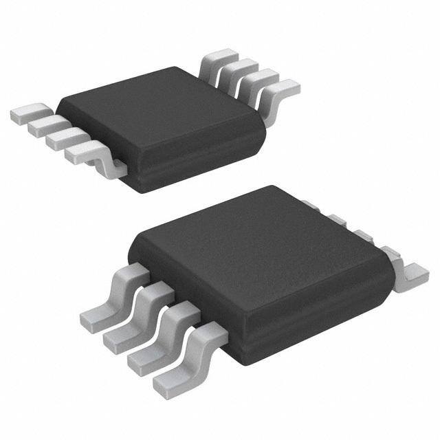
| 供应商器件封装 | 8-MSOP |
| 包装 | 管件 |
| 受监控电压数 | 3 |
| 复位 | 高有效/低有效 |
| 复位超时 | 最小为 140 ms |
| 安装类型 | 表面贴装 |
| 封装/外壳 | 8-TSSOP,8-MSOP(0.118",3.00mm 宽) |
| 工作温度 | -40°C ~ 85°C |
| 标准包装 | 80 |
| 电压-阈值 | 3.09V,4.649V,可调 |
| 类型 | 多压监控器 |
| 输出 | 开路漏极,推挽式 |


- 商务部:美国ITC正式对集成电路等产品启动337调查
- 曝三星4nm工艺存在良率问题 高通将骁龙8 Gen1或转产台积电
- 太阳诱电将投资9.5亿元在常州建新厂生产MLCC 预计2023年完工
- 英特尔发布欧洲新工厂建设计划 深化IDM 2.0 战略
- 台积电先进制程称霸业界 有大客户加持明年业绩稳了
- 达到5530亿美元!SIA预计今年全球半导体销售额将创下新高
- 英特尔拟将自动驾驶子公司Mobileye上市 估值或超500亿美元
- 三星加码芯片和SET,合并消费电子和移动部门,撤换高东真等 CEO
- 三星电子宣布重大人事变动 还合并消费电子和移动部门
- 海关总署:前11个月进口集成电路产品价值2.52万亿元 增长14.8%


PDF Datasheet 数据手册内容提取
DATASHEET ISL88021, ISL88022 FN8226 Triple Voltage Monitor with Adjustable Power-On-Reset and Rev 1.00 Undervoltage/Overvoltage Monitoring Capability September 18, 2006 The ISL88021 and ISL88022 family of devices are Features customizable triple voltage-monitoring supervisors that • Triple Voltage Monitor and Reset Assertion assert a reset if any of the monitored voltages becomes non-compliant. They offer popular functions such as • Low VDD Detection and Reset Assertion Power-On-Reset timing control with both RESET and - Adjustable Reset Threshold Voltages RESET outputs, Supply Voltage Supervision, both under or - 0.6V ±6mV Over -40°C to +85°C overvoltage detection, and Manual Reset assertion. By - Reset Signal Valid to VDD = 1V offering these features in a small 8 Ld MSOP package, the ISL88021 and ISL88022 can lower system cost, reduce • 140ms Minimum Reset Pulse Delay that is Customizable Using an External Capacitor board space requirements and increase the reliability of systems. • Both RST and RST Outputs Available Applying a voltage to VDD activates the Power-On-Reset • Undervoltage/Overvoltage Monitoring Capability circuit which holds RESET low for an adjustable period of • Low 20µA Consumption time. This allows the power supply and system oscillator to stabilize before the processor can execute code. • Small 8 Ld MSOP Package Low VDD detection circuitry protects the user’s system from • Pb-Free Plus Anneal Available (RoHS Compliant) low voltage conditions, resetting the system when VDD falls Applications below its minimum preset voltage threshold VTH1. Reset remains asserted until VDD returns to its proper operating • Process Control Systems level and stabilizes. Two additional voltage monitoring • Intelligent Instruments inputs, V2MON (preset) and V3MON (adjustable), monitor other supplies to provide reliable system operation. • Embedded Control Systems The ISL88021 V3MON input monitors for undervoltage (UV) • Computer Systems conditions whereas the ISL88022 V3MON input allows • Portable/Battery-Powered Equipment monitoring for overvoltage (OV) conditions. The monitored • Multi-Voltage Systems voltage on V3MON on either device is compared via a resistor divider to a 600mV internal reference. Hence, any Pinout voltage more or less positive than this reference can be accurately monitored to meet specific system level ISL88021, ISL88022 (8 LD MSOP) requirements or to fine-tune the threshold for applications TOP VIEW requiring higher precision. These devices also let users increase the Power-On-Reset MR 1 8 RST time-out delay by connecting a capacitor between CPOR and ground. This lengthens the period of an internal clock VDD 2 7 RST counter thereby increasing the time between voltage compliance and reset outputs signaling. V2MON 3 6 CPOR A manual reset input provides debounce circuitry for GND 4 5 V3MON minimum reset component count. FN8226 Rev 1.00 Page 1 of 8 September 18, 2006
ISL88021, ISL88022 Ordering Information Ordering Information (See Notes) (See Notes) (Continued) PART PART VDD V2MO V3MON PART PART VDD V2MO V3MON NUMBER MARKING VTRIP1 VTRIP2 TYPE PACKAGE NUMBER MARKING VTRIP1 VTRIP2 TYPE PACKAGE ISL88021IU8FAZ ANM 3.09V 1.69V UV 8 Ld MSOP ISL88022IU8HAZ 4.64V 1.69V OV 8 Ld MSOP ISL88021IU8FCZ ANL 3.09V 2.32V UV 8 Ld MSOP ISL88022IU8HCZ 4.64V 2.32V OV 8 Ld MSOP ISL88021IU8FEZ 3.09V 2.92V UV 8 Ld MSOP ISL88022IU8HEZ ANO 4.64V 2.92V OV 8 Ld MSOP ISL88021IU8FFZ 3.09V 3.09V UV 8 Ld MSOP ISL88022IU8HFZ ANN 4.64V 3.09V OV 8 Ld MSOP ISL88021IU8HAZ 4.64V 1.69V UV 8 Ld MSOP NOTES: ISL88021IU8HCZ 4.64V 2.32V UV 8 Ld MSOP 1. Standard versions are shown in bold. For non-standard versions, please contact factory for availability. ISL88021IU8HEZ ANK 4.64V 2.92V UV 8 Ld MSOP 2. Add “-TK” suffix for Tape and Reel. ISL88021IU8HFZ ANJ 4.64V 3.09V UV 8 Ld MSOP 3. Intersil Pb-free plus anneal products employ special Pb-free ISL88022IU8FAZ ANQ 3.09V 1.69V OV 8 Ld MSOP material sets; molding compounds/die attach materials and 100% matte tin plate termination finish, which are RoHS compliant and ISL88022IU8FCZ ANP 3.09V 2.32V OV 8 Ld MSOP compatible with both SnPb and Pb-free soldering operations. ISL88022IU8FEZ 3.09V 2.92V OV 8 Ld MSOP Intersil Pb-free products are MSL classified at Pb-free peak reflow temperatures that meet or exceed the Pb-free requirements of ISL88022IU8FFZ 3.09V 3.09V OV 8 Ld MSOP IPC/JEDEC J STD-020. Block Diagrams VDD RST VDD RST RST RST POR POR V2MON V2MON CPOR CPOR MR MR V3MON V3MON PB PB ± VREF ± VREF GND GND ISL88021 ISL88022 Pin Descriptions ISL88021 ISL88022 NAME FUNCTION 1 1 MR Active-Low Open Drain Manual Reset Input 2 2 VDD Power Supply Input 3 3 V2MON Second Undervoltage Monitor Input 4 4 GND Ground 5 V3MON Undervoltage Monitor Input 5 V3MON Overvoltage Monitor Input 6 6 CPOR Set Power-On-Reset Timeout Delay 7 7 RST Active-Low Open Drain Reset Output 8 8 RST Active-High Push-Pull Reset Output FN8226 Rev 1.00 Page 2 of 8 September 18, 2006
ISL88021, ISL88022 Absolute Maximum Ratings Thermal Information Temperature Under Bias . . . . . . . . . . . . . . . . . . . . . .-40°C to +85°C Thermal Resistance (Typical, Note 1) JA (°C/W) Voltage on Any Pin with Respect to GND . . . . . . . . . . .-1.0V to +7V MSOP Package . . . . . . . . . . . . . . . . . . . . . . . . . . . . 145 D.C. Output Current. . . . . . . . . . . . . . . . . . . . . . . . . . . . . . . . . . 5mA Maximum Junction Temperature (Plastic Package) . . . . . . .+150°C Maximum Storage Temperature Range. . . . . . . . . .-65°C to +150°C Recommended Operating Conditions Maximum Lead Temperature (Soldering 10s) . . . . . . . . . . . .+300°C (MSOP - Lead Tips Only) Industrial . . . . . . . . . . . . . . . . . . . . . . . . . . . . . . . . . .-40°C to +85°C CAUTION: Stresses above those listed in “Absolute Maximum Ratings” may cause permanent damage to the device. This is a stress only rating and operation of the device at these or any other conditions above those indicated in the operational sections of this specification is not implied. NOTE: 1. JA is measured with the component mounted on a high effective thermal conductivity test board in free air. See Tech Brief TB379 for details. Electrical Specifications Over the recommended operating conditions unless otherwise specified. SYMBOL PARAMETER TEST CONDITIONS MIN TYP MAX UNITS VDD Supply Voltage Range 2.0 5.5 V IDD1 VDD Supply Current VDD = 5.0V 12.5 15 µA IDD2 V2MON Input Current V2MON = 3.3V 5.5 6 µA IDDA V3MON Input Current V3MON = 1.0V 19 100 nA VOLTAGE THRESHOLDS VTH1 Fixed Voltage Trip Point for VDD ISL88021/22IU8HxZ 4.565 4.649 4.733 V ISL88021/22IU8FxZ 3.029 3.085 3.141 V VTH1HYST Hysteresis of VTH1 VTH1 = 4.64V 46 mV VTH1 = 3.09V 37 mV VTH2 Fixed Voltage Trip Point for V2MON ISL88021/22IU8xFZ 3.034 3.090 3.146 V ISL88021/22IU8xEZ 2.894 2.947 3.000 V ISL88021/22IU8xCZ 2.290 2.332 2.374 V ISL88021/22IU8xAZ 1.660 1.690 1.720 V VTH2HYST Hysteresis of VTH2 VTH2 = 3.09V 37 mV VTH2 = 2.92V 29 mV VTH2 = 2.32V 23 mV VTH2 = 2.19V 22 mV VTH2 = 1.69V 17 mV VTH3 V3MON Threshold Voltage VTH for V3MON on ISL88021 0.594 0.605 0.616 V VTH for V3MON on ISL88022 0.587 0.595 0.603 V VREFHYST Hysteresis Voltage 3 mV RESET VOL Reset Output Voltage Low VDD 3.3V, Sinking 2.5mA 0.05 0.40 V VDD < 3.3V, Sinking 1.5mA 0.05 0.40 V VOH RST Output Voltage High VDD 3.3V, Sourcing 2.5mA VDD-0.6 VDD-0.4 V VDD < 3.3V, Sourcing 1.5mA VDD-0.6 VDD-0.4 V tRPD VTH to Reset Asserted Delay 10 µs tPOR POR Timeout Delay CPOR is open 140 200 ms CLOAD Load Capacitance on Reset Pins 5 pF FN8226 Rev 1.00 Page 3 of 8 September 18, 2006
ISL88021, ISL88022 Electrical Specifications Over the recommended operating conditions unless otherwise specified. (Continued) SYMBOL PARAMETER TEST CONDITIONS MIN TYP MAX UNITS MANUAL RESET VMRL MR Input Voltage Low 0.8 V VMRH MR Input Voltage High VDD-0.6 V tMR MR Minimum Pulse Width 550 ns RPU Internal Pull-Up Resistor 20 k Functional Description Power-On-Reset (POR) The ISL88021 and ISL88022 devices incorporate such features Applying power to the ISL88021 and ISL88022 devices activates as Power-On-Reset control, Supply Voltage Supervision, a POR circuit which holds the RESET pin low once VDD > 1V. Undervoltage or Overvoltage Monitoring, and Manual Reset This signal provides several benefits: Assertion. • It prevents the system microprocessor from starting to operate with insufficient voltage. The ISL88021 and ISL88022 devices provide common preset threshold voltages on both VDD and V2MON and for an optional • It prevents the processor from operating prior to resistor divider network on V3MON to provide custom voltage stabilization of the oscillator. monitoring of voltages greater than 0.6V. An optional capacitor • It ensures that the monitored device is held out of operation can be connected between the CPOR pin and GND to increase until internal registers are properly loaded. the nominal 200ms tPOR delay. Figure 7 illustrates operational functionality with a timing diagram. • It allows time for an FPGA to download its configuration prior to initialization of the circuit. Voltage Monitoring When all of the monitored voltages meet their respective input During normal operation, the ISL88021 and ISL88022 monitor the voltage requirements for the specified reset timeout delay voltage levels on VDD, V2MON and V3MON. The ISL88021 tPOR, the POR circuit simultaneously pulls the RST output low asserts reset if any one of these voltages fall below their and releases the RST output to allow the system to begin respective voltage trip points and in the case of ISL88022 above operation. the voltage trip point on the V3MON input. The reset signal effectively prevents the microprocessor from operating during a Adjusting tPOR power failure, brownout or over voltage condition. This signal On the ISL88021 and ISL88022, users can adjust the Power- remains active until all monitored voltages meet all voltage On-Reset timeout delay (tPOR) to many times the nominal threshold requirements for the reset time delay period tPOR. Note tPOR. Figure 2 illustrates the effect of capacitance on the CPOR that both RESET and RESET signals are provided for design pin to ground, showing changing tPOR with a graph normalized flexibility. Figure 1 illustrates the VDD, V2MON and V3MON input to 175ms for an open CPOR pin. The maximum recommended threshold voltages for the various available options. capacitance that should be placed on the CPOR pin is 50pF. NOTE: Care should be taken in PCB layout and capacitor placement in order to eliminate stray capacitance as much as 5.000 V) 4.500 Vth = 4.64V possible, which contributes to tPOR error. h ( 4.000 Vt N 3.500 Vth = 3.09V 10 O M 3.000 V3 2.500 Vth = 2.92V OR 8 2MON, 12..500000 VVtthh == 12..6392VV zed tP 6 D, V 1.000 mali 4 D V 0.500 Vth = 0.60V Nor 2 0.000 -40 25 85 0 TEMPERATURE (°C) 1 5 9 13 17 21 25 29 33 37 41 45 FIGURE 1. VDD, V2MON, V3MON VTH vs TEMP C (pF) POR FIGURE 2. NORMALIZED tPOR vs CPOR GRAPH FN8226 Rev 1.00 Page 4 of 8 September 18, 2006
ISL88021, ISL88022 Manual Reset The manual reset input (MR) allows the user to trigger a reset by using a push-button switch or by signaling that pin low. The MR input is an active low debounced input. By connecting a push- button directly from MR to ground, the designer adds manual system reset capability. Reset is asserted if the MR pin is pulled low to less than 100mV for 1µs or longer while the push-button is closed or a reset is signaled. After MR is released, the reset outputs remain asserted for tPOR. MR input has an internal 20k ISL88021IU8HFZ pull up resistor provided. Figure 3 illustrates a typical application diagram for either IC showing both reset outputs being used along with both a manual and signalled reset configuration. The VDD and V2MON thresholds are preset whereas the V3MON is capable of UV (ISL88021) or OV (ISL88022) monitoring of a voltage greater than or less than 0.6V, respectively. TO DISPLAY 3.3V - 5V VDD RST TO µP RST ISL88022IU8HFZ V2MON 1.8V - 3.3V MR RESET ISL88021 PB SIGNAL ISL88022 V3MON CPOR VMON > 0.6V GND FIGURE 3. TYPICAL APPLICATION DIAGRAM Application Considerations Follow good decoupling practices to prevent transients from causing unwanted reset signaling due to switching noises and FIGURE 4. ISL88021_22EVAL1 SCHEMATIC AND PHOTO short duration droops. When using the CPOR pin, reduce layout stray capacitance on this pin to minimize effect on tPOR timing. If no PCB CPOR pad is patterned, the tPOR can be 160ms. MONITORED VOLTAGE RISING AND FALLING RAMP THROUGH THE PROGRAMMED UV AND OV THRESHOLDS Using the ISL88021_22EVAL1 Platform The ISL88021_22EVAL1 board is designed to provide both immediate functional assessment and flexibility to the user. Both ICs are the ‘HF’ variant having a VDD Vth of 4.64V, a V2MON Vth of 3.09V and V3MON Vth of 0.6V. The top IC position is the ISL88021 and is configured to monitor for undervoltage (UV) compliance of a 5V, 3.3V and a 2.5V and signaling the RESET and RESET outputs. The bottom position is the ISL88022 RESET# RESPONDING TO variant, which is configured to measure a 3.3V overvoltage MONITORED VOLTAGE. CPOR PIN IS OPEN, tPOR = 150ms (OV) in addition to UV on both the 5V and 3.3V supplies. RESET and RESET is asserted for at least tPOR when these voltage go out of range. In both cases V3MON interfaces with the monitored supply via a simple resistor divider for comparison to the internal 0.6V reference. A Manual Reset (MR) input is FIGURE 5. ISL88022EVAL1 3.3V UV AND OV DETECTION provided on both ICs and is invoked by pulling this input LOW. FN8226 Rev 1.00 Page 5 of 8 September 18, 2006
ISL88021, ISL88022 3.3V RISING EDGE 100ms/DIV ISL88022 tPOR = 150ms CPOR = OPEN ISL88021 tPOR = 390ms CPOR = 10pF FIGURE 6. ISL88021_22EVAL1 tPOR COMPARISON Operational Timing Diagrams VTH1 VDD 1V V2MON or V3MON (ISL88021) VTH2 or VREF >tMR MR tPOR tRPD tPOR tRPD tPOR tPOR RST RST <tMD FIGURE 7. ISL88021 AND ISL88022 TIMING DIAGRAM FN8226 Rev 1.00 Page 6 of 8 September 18, 2006
ISL88021, ISL88022 © Copyright Intersil Americas LLC 2006. All Rights Reserved. All trademarks and registered trademarks are the property of their respective owners. For additional products, see www.intersil.com/en/products.html Intersil products are manufactured, assembled and tested utilizing ISO9001 quality systems as noted in the quality certifications found at www.intersil.com/en/support/qualandreliability.html Intersil products are sold by description only. Intersil may modify the circuit design and/or specifications of products at any time without notice, provided that such modification does not, in Intersil's sole judgment, affect the form, fit or function of the product. Accordingly, the reader is cautioned to verify that datasheets are current before placing orders. Information furnished by Intersil is believed to be accurate and reliable. However, no responsibility is assumed by Intersil or its subsidiaries for its use; nor for any infringements of patents or other rights of third parties which may result from its use. No license is granted by implication or otherwise under any patent or patent rights of Intersil or its subsidiaries. For information regarding Intersil Corporation and its products, see www.intersil.com FN8226 Rev 1.00 Page 7 of 8 September 18, 2006
ISL88021, ISL88022 Mini Small Outline Plastic Packages (MSOP) N M8.118 (JEDEC MO-187AA) 8 LEAD MINI SMALL OUTLINE PLASTIC PACKAGE INCHES MILLIMETERS E1 E SYMBOL MIN MAX MIN MAX NOTES A 0.037 0.043 0.94 1.10 - -B- INDEX AREA 1 2 0.20 (0.008) A B C A1 0.002 0.006 0.05 0.15 - TOP VIEW A2 0.030 0.037 0.75 0.95 - 4X b 0.010 0.014 0.25 0.36 9 0.25 R1 (0.010) R c 0.004 0.008 0.09 0.20 - GAUGE D 0.116 0.120 2.95 3.05 3 PLANE E1 0.116 0.120 2.95 3.05 4 SEATING L e 0.026 BSC 0.65 BSC - PLANE -C- 4X A A2 L1 E 0.187 0.199 4.75 5.05 - L 0.016 0.028 0.40 0.70 6 SEATING L1 0.037 REF 0.95 REF - 0.10 (0.004) C PLANE -H- b N 8 8 7 A1 -A- e R 0.003 - 0.07 - - D 0.20 (0.008) C C R1 0.003 - 0.07 - - SIDE VIEW a 0 5o 15o 5o 15o - CL 0o 6o 0o 6o - E1 -B- Rev. 2 01/03 0.20 (0.008) C D END VIEW NOTES: 1. These package dimensions are within allowable dimensions of JEDEC MO-187BA. 2. Dimensioning and tolerancing per ANSI Y14.5M-1994. 3. Dimension “D” does not include mold flash, protrusions or gate burrs and are measured at Datum Plane. Mold flash, protrusion and gate burrs shall not exceed 0.15mm (0.006 inch) per side. 4. Dimension “E1” does not include interlead flash or protrusions and are measured at Datum Plane. - H - Interlead flash and protrusions shall not exceed 0.15mm (0.006 inch) per side. 5. Formed leads shall be planar with respect to one another within 0.10mm (0.004) at seating Plane. 6. “L” is the length of terminal for soldering to a substrate. 7. “N” is the number of terminal positions. 8. Terminal numbers are shown for reference only. 9. Dimension “b” does not include dambar protrusion. Allowable dambar protrusion shall be 0.08mm (0.003 inch) total in excess of “b” dimension at maximum material condition. Minimum space between protrusion and adjacent lead is 0.07mm (0.0027 inch). 10. Datums -A - and - B - to be determined at Datum plane - H - . 11. Controlling dimension: MILLIMETER. Converted inch dimen- sions are for reference only. FN8226 Rev 1.00 Page 8 of 8 September 18, 2006