ICGOO在线商城 > 集成电路(IC) > 接口 - 模拟开关,多路复用器,多路分解器 > ISL84781IRZ

 Datasheet下载
- 型号: ISL84781IRZ
- 制造商: Intersil
- 库位|库存: xxxx|xxxx
- 要求:
| 数量阶梯 | 香港交货 | 国内含税 |
| +xxxx | $xxxx | ¥xxxx |
查看当月历史价格
查看今年历史价格
ISL84781IRZ产品简介:
ICGOO电子元器件商城为您提供ISL84781IRZ由Intersil设计生产,在icgoo商城现货销售,并且可以通过原厂、代理商等渠道进行代购。 ISL84781IRZ价格参考。IntersilISL84781IRZ封装/规格:接口 - 模拟开关,多路复用器,多路分解器, 1 Circuit IC Switch 8:1 750mOhm 16-TQFN (3x3)。您可以下载ISL84781IRZ参考资料、Datasheet数据手册功能说明书,资料中有ISL84781IRZ 详细功能的应用电路图电压和使用方法及教程。
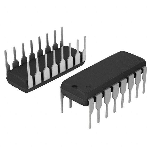
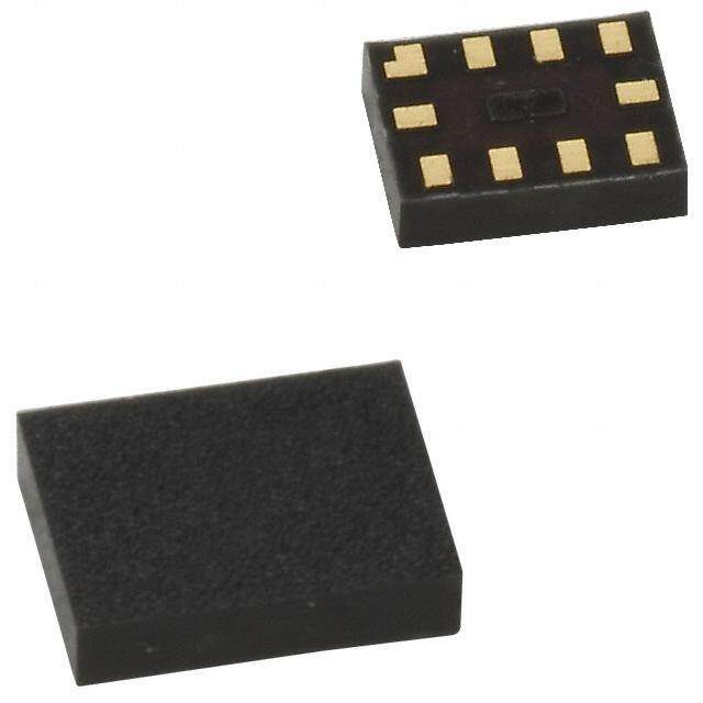
ISL84781IRZ是Renesas Electronics America Inc.生产的一款模拟开关,属于接口类器件中的多路复用器/多路分解器。该器件为单通道双刀双掷(DPDT)配置,具有低导通电阻和宽电源电压范围(±5V至±20V),支持双向信号传输,适用于需要切换或路由模拟信号的场景。

典型应用场景包括工业自动化、测试测量设备和通信系统。在工业控制中,可用于切换传感器信号或执行器控制线路;在自动测试设备(ATE)中,可实现多路信号的选通与路由,提高测试效率;在音频或视频信号切换系统中,因其低失真和高带宽特性,适合高质量模拟信号的切换。此外,该器件也适用于数据采集系统,用于多通道信号的分时采集与处理。

ISL84781IRZ采用TSSOP-16封装,体积小,便于集成于紧凑型电路板中。其高可靠性与稳定的电气性能使其在恶劣工作环境下仍能保持良好表现,广泛应用于需高精度模拟信号管理的领域。
| 参数 | 数值 |
| 产品目录 | 集成电路 (IC)半导体 |
| 描述 | IC MUX/DEMUX 8X1 16TQFN多路器开关 IC ANALOG SWITCH 8:1 0 3OHM S 1 65V |
| 产品分类 | |
| 品牌 | Intersil |
| 产品手册 | |
| 产品图片 |
|
| rohs | 符合RoHS无铅 / 符合限制有害物质指令(RoHS)规范要求 |
| 产品系列 | 开关 IC,多路器开关 IC,Intersil ISL84781IRZ- |
| 数据手册 | |
| 产品型号 | ISL84781IRZ |
| PCN组件/产地 | |
| 产品目录页面 | |
| 产品种类 | 多路器开关 IC |
| 传播延迟时间 | 28 ns at 2.7 V, 34 ns at 1.8 V |
| 供应商器件封装 | 16-TQFN(3x3) |
| 关闭隔离—典型值 | 65 dB |
| 功能 | 多路复用器/多路分解器 |
| 包装 | 管件 |
| 商标 | Intersil |
| 安装类型 | 表面贴装 |
| 安装风格 | SMD/SMT |
| 导通电阻 | 750 毫欧 |
| 导通电阻—最大值 | 0.55 Ohms |
| 封装 | Tube |
| 封装/外壳 | 16-WFQFN 裸露焊盘 |
| 封装/箱体 | TQFN-16 |
| 工作温度 | -40°C ~ 85°C |
| 工作电源电压 | 1.6 V to 3.6 V |
| 工作电源电流 | 0.05 uA |
| 工厂包装数量 | 100 |
| 带宽 | 52 MHz |
| 开关数量 | 1 |
| 最大工作温度 | + 85 C |
| 最小工作温度 | - 40 C |
| 标准包装 | 100 |
| 电压-电源,单/双 (±) | 1.6 V ~ 3.6 V |
| 电压源 | 单电源 |
| 电流-电源 | 50nA |
| 电路 | 1 x 8:1 |
| 空闲时间—最大值 | 14 ns |
| 系列 | ISL84781 |
| 运行时间—最大值 | 16 ns |
| 通道数量 | 8 Channel |


- 商务部:美国ITC正式对集成电路等产品启动337调查
- 曝三星4nm工艺存在良率问题 高通将骁龙8 Gen1或转产台积电
- 太阳诱电将投资9.5亿元在常州建新厂生产MLCC 预计2023年完工
- 英特尔发布欧洲新工厂建设计划 深化IDM 2.0 战略
- 台积电先进制程称霸业界 有大客户加持明年业绩稳了
- 达到5530亿美元!SIA预计今年全球半导体销售额将创下新高
- 英特尔拟将自动驾驶子公司Mobileye上市 估值或超500亿美元
- 三星加码芯片和SET,合并消费电子和移动部门,撤换高东真等 CEO
- 三星电子宣布重大人事变动 还合并消费电子和移动部门
- 海关总署:前11个月进口集成电路产品价值2.52万亿元 增长14.8%


PDF Datasheet 数据手册内容提取
DATASHEET ISL84781 FN6095 Ultra Low ON-Resistance, Low-Voltage, Single Supply, 8-to-1 Analog Multiplexer Rev 4.00 October 28, 2010 The Intersil ISL84781 device contains precision, bidirectional, Features analog switches configured as an 8-channel • Pin Compatible Replacement for the MAX4781, and multiplexer/demultiplexer. It is designed to operate from a MAX4617 single +1.6V to +3.6V supply. The device has an inhibit pin to simultaneously open all signal paths. • ON-resistance (rON) - V+ = +3.0V . . . . . . . . . . . . . . . . . . . . . . . . . . . . . . 0.4 ON-resistance is 0.4 with a +3.0V supply and 0.55 with a - V+ = +1.8V . . . . . . . . . . . . . . . . . . . . . . . . . . . . . 0.55 single +1.8V supply. Each switch can handle rail-to-rail analog signals. The off-leakage current is only 4nA max at • rON Matching Between Channels . . . . . . . . . . . . . . . . 0.12 +25°C or 40nA max at +85°C with a +3.3V supply. • rON Flatness Across Signal Range . . . . . . . . . . . . . . .0.056 All digital inputs are 1.8V logic-compatible when using a • Single Supply Operation. . . . . . . . . . . . . . . . . +1.6V to +3.6V single +3V supply. • Low Power Consumption (PD). . . . . . . . . . . . . . . . . . <0.2µW The ISL84781 is a 8-to-1 multiplexer device that is offered in a • Fast Switching Action (VS = +3V) 16 Ld TSSOP package, and a 16 Ld thin QFN package. - tON . . . . . . . . . . . . . . . . . . . . . . . . . . . . . . . . . . . . .16ns Table 1 summarizes the performance of this family. - tOFF . . . . . . . . . . . . . . . . . . . . . . . . . . . . . . . . . . . .13ns TABLE 1. FEATURES AT A GLANCE • Guaranteed Break-Before-Make ISL84781 • High Current Handling Capacity (300mA Continuous) Configuration 8:1 Mux • Available in 16 Ld TSSOP and 16 Ld 3x3 Thin QFN 3V rON • 1.8V CMOS-Logic Compatible (+3V Supply) 3V tON/tOFF 16ns/13ns • Pb-Free (RoHS Compliant) 1.8V rON 0.55 • ISL84781IR Replaces the ISL43L680IR. 1.8V tON/tOFF 24ns/16ns Applications Packages 16 Ld TSSOP, 16 Ld 3x3 thin QFN • Battery Powered, Handheld, and Portable Equipment Related Literature - Cellular/Mobile Phones - Pagers • Technical Brief TB363 “Guidelines for Handling and Processing Moisture Sensitive Surface Mount Devices - Laptops, Notebooks, Palmtops (SMDs)” • Portable Test and Measurement • Application Note AN557 “Recommended Test Procedures • Medical Equipment for Analog Switches” • Audio Switching and Routing Pinouts (Note 1) ISL84781 ISL84781 (16 LD TSSOP) (16 LD 3x3 THIN QFN) TOP VIEW TOP VIEW 6 4 2 NO4 1 16 V+ NO NO V+ NO NO6 2 15 NO2 16 15 14 13 COM 3 14 NO1 COM 1 12 NO1 NO7 4 13 NO0 NO7 2 11 NO0 NO5 5 12 NO3 NO5 3 10 NO3 INH 6 LOGIC 11 ADD0 N.C. 7 10 ADD1 INH 4 9 ADD0 GND 8 9 ADD2 5 6 7 8 N.C. GND DD2 DD1 A A FN6095 Rev 4.00 Page 1 of 12 October 28, 2010
ISL84781 Pinouts (Note 1) (Continued) NOTE: 1. Switches Shown for Logic “0” Inputs. Truth Table Ordering Information ISL84781 PART TEMP. NUMBER PART RANGE PACKAGE PKG. INH ADD2 ADD1 ADD0 SWITCH ON (Notes 2, 3, 4) MARKING (°C) (Pb-free) DWG. # 1 X X X NONE ISL84781IVZ 84781 IVZ -40 to +85 16 Ld TSSOP M16.173 0 0 0 0 NO0 ISL84781IRZ 781Z -40 to +85 16 Ld TQFN L16.3x3A 0 0 0 1 NO1 2. Add “-T*” suffix for tape and reel. Please refer to TB347 for 0 0 1 0 NO2 details on reel specifications. 3. Intersil Pb-free products employ special Pb-free material sets; 0 0 1 1 NO3 molding compounds/die attach materials and 100% matte tin 0 1 0 0 NO4 plate termination finish, which are RoHS compliant and compatible with both SnPb and Pb-free soldering operations. 0 1 0 1 NO5 Intersil Pb-free products are MSL classified at Pb-free peak reflow temperatures that meet or exceed the Pb-free 0 1 1 0 NO6 requirements of IPC/JEDEC J STD-020C. 0 1 1 1 NO7 4. For Moisture Sensitivity Level (MSL), please see device NOTE: Logic “0” 0.5V. Logic “1” 1.4V, with a 3V supply. X = Don’t information page for ISL84781. For more information on MSL, Care. please see Technical Brief TB363. Pin Descriptions PIN FUNCTION V+ System Power Supply Input (1.6V to 3.6V) N.C. No Connect. Not internally connected. GND Ground Connection INH Digital Control Input. Connect to GND for Normal Operation. Connect to V+ to turn all switches off. COM Analog Switch Common Pin NO0 - Analog Switch Input Pin NO7 ADD Address Input Pin FN6095 Rev 4.00 Page 2 of 12 October 28, 2010
ISL84781 Absolute Maximum Ratings Thermal Information V+ to GND. . . . . . . . . . . . . . . . . . . . . . . . . . . . . . . . . . . -0.3 to 4.7V Thermal Resistance (Typical, Note 6) JA (°C/W) Input Voltages 16 Ld TSSOP Package . . . . . . . . . . . . . . . . . . . . . . 150 INH, NO, ADD (Note 5) . . . . . . . . . . . . . . . . . -0.3 to (V+) + 0.3V 16 Ld 3x3 Thin QFN Package . . . . . . . . . . . . . . . . . 75 Output Voltages Maximum Junction Temperature (Plastic Package). . . . . . . +150°C COM (Note 5). . . . . . . . . . . . . . . . . . . . . . . . . -0.3 to (V+) + 0.3V Maximum Storage Temperature Range. . . . . . . . . . . -65°C to +150°C Continuous Current NO or COM . . . . . . . . . . . . . . . . . . . . . ±300mA Pb-Free Reflow Profile. . . . . . . . . . . . . . . . . . . . . . . . .see link below Peak Current NO or COM http://www.intersil.com/pbfree/Pb-FreeReflow.asp (Pulsed 1ms, 10% Duty Cycle, Max) . . . . . . . . . . . . . . . . ±500mA ESD Rating Operating Conditions Human Body Model . . . . . . . . . . . . . . . . . . . . . . . . . . . . . . . >4kV Machine Model. . . . . . . . . . . . . . . . . . . . . . . . . . . . . . . . . . >300V Temperature Range. . . . . . . . . . . . . . . . . . . . . . . . . -40°C to +85°C Charged Device Model. . . . . . . . . . . . . . . . . . . . . . . . . . . >1000V CAUTION: Do not operate at or near the maximum ratings listed for extended periods of time. Exposure to such conditions may adversely impact product reliability and result in failures not covered by warranty. NOTES: 5. Signals on NO, COM, ADD, or INH exceeding V+ or GND are clamped by internal diodes. Limit forward diode current to maximum current ratings. 6. JA is measured with the component mounted on a high effective thermal conductivity test board in free air. See Tech Brief TB379 for details. Electrical Specifications - 3V Supply Test Conditions: VSUPPLY = +2.7V to +3.3V, GND = 0V, VINH = 1.4V, VINL = 0.5V (Note 7), Unless Otherwise Specified. Boldface limits apply over the operating temperature range, -40°C to +85°C. TEMP MIN MAX PARAMETER TEST CONDITIONS (°C) (Notes 8, 11) TYP (Notes 8, 11) UNITS ANALOG SWITCH CHARACTERISTICS Analog Signal Range, VANALOG Full 0 - V+ V ON-resistance, rON V+ = 2.7V, ICOM = 100mA, VNO = V to V+, 25 - 0.41 0.75 (See Figure 5) Full - - 0.8 rON Matching Between Channels, V+ = 2.7V, ICOM = 100mA, VNO = Voltage at max 25 - 0.12 0.2 rON rON, (Note 9) Full - - 0.2 rON Flatness, RFLAT(ON) V+ = 2.7V, ICOM = 100mA, VNO = V to V+, 25 - 0.056 0.15 (Note 10) Full - - 0.15 NO OFF Leakage Current, INO(OFF) V+ = 3.3V, VCOM = 0.3V, 3V, VNO = 3V, 0.3V 25 -4 - 4 nA Full -40 - 40 nA COM ON Leakage Current, V+ = 3.3V, VCOM = VNO = 0.3V, 3V 25 -15 - 15 nA ICOM(ON) Full -70 - 70 nA DIGITAL INPUT CHARACTERISTICS Input Voltage High, VINH, VADDH Full 1.4 - - V Input Voltage Low, VINL, VADDL Full - - 0.5 V Input Current, IINH, IINL, IADDH, V+ = 3.6V, VINH = VADD = 0V or V+ (Note 12) Full -0.5 - 0.5 µA IADDL DYNAMIC CHARACTERISTICS Inhibit Turn-ON Time, tON V+ = 2.7V, VNO = V, RL = 50, CL = 35pF, 25 - 16 25 ns (SeeFigure 1, Note 12) Full - - 27 ns Inhibit Turn-OFF Time, tOFF V+ = 2.7V, VNO = 1.5V, RL = 50, CL = 35pF, 25 - 14 23 ns (SeeFigure 1, Note 12) Full - - 25 ns Address Transition Time, tTRANS V+ = 2.7V, VNO = 1.5V, RL = 50, CL = 35pF, 25 - 19 28 ns (SeeFigure 1, Note 12) Full - - 30 ns Break-Before-Make Time, tBBM V+ = 3.3V, VNO = 1.5V, RL = 50, CL = 35pF, 25 - 4 - ns (SeeFigure 3, Note 12) Full 1 - - ns Charge Injection, Q CL = 1.0nF, VG = 0V, RG = 0, (See Figure 2) 25 - -39 - pC Input OFF Capacitance, COFF f = 1MHz, VNO = VCOM = 0V, (See Figure 6) 25 - 65 - pF FN6095 Rev 4.00 Page 3 of 12 October 28, 2010
ISL84781 Electrical Specifications - 3V Supply Test Conditions: VSUPPLY = +2.7V to +3.3V, GND = 0V, VINH = 1.4V, VINL = 0.5V (Note 7), Unless Otherwise Specified. Boldface limits apply over the operating temperature range, -40°C to +85°C. (Continued) TEMP MIN MAX PARAMETER TEST CONDITIONS (°C) (Notes 8, 11) TYP (Notes 8, 11) UNITS COM OFF Capacitance, COFF f = 1MHz, VNO = VCOM = 0V, (See Figure 6) 25 - 470 - pF COM ON Capacitance, CCOM(ON) f = 1MHz, VNO = VCOM = 0V, (See Figure 6) 25 - 485 - pF OFF-Isolation RL = 50, CL = 35pF, f = 100kHz, (See Figure 4) 25 - 65 - dB Total Harmonic Distortion (THD) f = 20Hz to 20kHz, 0.5VP-P, RL = 32 25 - 0.014 - % POWER SUPPLY CHARACTERISTICS Power Supply Range Full 1.6 - 3.6 V Positive Supply Current, I+ V+ = 3.6V, VINH, VADD = 0V or V+, Switch On or Off 25 - - 0.05 µA Full - - 1.2 µA NOTES: 7. VIN = Input voltage to perform proper function. 8. The algebraic convention, whereby the most negative value is a minimum and the most positive a maximum, is used in this data sheet. 9. rON matching between channels is calculated by subtracting the channel with the highest max rON value from the channel with lowest max rON value. 10. Flatness is defined as the difference between maximum and minimum value of on-resistance over the specified analog signal range. 11. Parameters with MIN and/or MAX limits are 100% tested at +25°C, unless otherwise specified. Temperature limits established by characterization and are not production tested. 12. Limits established by characterization and are not production tested. Electrical Specifications: 1.8V Supply Test Conditions: V+ = +1.8V, GND = 0V, VINH = 1V, VINL = 0.4V (Note 7), Unless Otherwise Specified. Boldface limits apply over the operating temperature range, -40°C to +85°C. TEMP MIN MAX PARAMETER TEST CONDITIONS (°C) (Notes 8, 11) TYP (Notes 8, 11) UNITS ANALOG SWITCH CHARACTERISTICS Analog Signal Range, VANALOG Full 0 - V+ V ON-resistance, rON V+ = 1.8V, ICOM = 10.0mA, VNO = 1.0V, 25 - 0.55 0.85 (See Figure 5) Full - - 0.9 rON Matching Between Channels, V+ = 1.8V, ICOM = 10.0mA, VNO = 1.0V, 25 - 0.1 - rON) (See Figure 5) Full - 0.13 - rON Flatness, RFLAT(ON) V+ = 1.8V, ICOM = 10.0mA, VNO = 0V, 0.9V, 1.6V, 25 - 0.14 - (See Figure 5) Full - 0.16 - DIGITAL INPUT CHARACTERISTICS Input Voltage High, VINH, VADDH Full 1 - - V Input Voltage Low, VINL, VADDL Full - - 0.4 V Input Current, IINH, IINL, IADDH, V+ = 1.8V, VINH, VADD = 0V or V+ (Note 12) Full -0.5 - 0.5 A IADDL DYNAMIC CHARACTERISTICS Inhibit Turn-ON Time, tON V+ = 1.8V, VNO = 1.0V, RL = 50, CL = 35pF, 25 - 24 33 ns (SeeFigure 1, Note 12) Full - - 35 ns Inhibit Turn-OFF Time, tOFF V+ = 1.8V, VNO = 1.0V, RL = 50, CL = 35pF, 25 - 16 25 ns (SeeFigure 1, Note 12) Full - - 27 ns Address Transition Time, tTRANS V+ = 1.8V, VNO = 1.0V, RL = 50, CL = 35pF, 25 - 25 34 ns (SeeFigure 1, Note 12) Full - - 36 ns Break-Before-Make Time, tBBM V+ = 1.8V, VNO = 1.0V, RL = 50, CL = 35pF, 25 - 9 - ns (See Figure 3, Note 12) Charge Injection, Q CL = 1.0nF, VG = 0V, RG = 0(See Figure 2) 25 - -20 - pC FN6095 Rev 4.00 Page 4 of 12 October 28, 2010
ISL84781 Test Circuits and Waveforms V+ C C V+ tr < 5ns LOGIC 50% tf < 5ns INPUT 0V VNO0 NO0 tON NO1-NO7 COM VOUT INH VNO0 90% VOUT 90% LOGIC GND ADD2-0 RL CL SWITCH INPUT 50 35pF OUTPUT 0V tOFF Logic input waveform is inverted for switches that have the opposite Repeat test for other switches. CL includes fixture and stray logic sense. capacitance. R L V = V ------------------------ OUT NOx R +r L ON FIGURE 1A. INHIBIT tON/tOFF MEASUREMENT POINTS FIGURE 1B. INHIBIT tON/tOFF TEST CIRCUIT V+ V+ tr < 5ns C C LOGIC 50% tf < 5ns INPUT 0V tTRANS VNO0 NO0 VOUT COM NO1-NO7 VNO0 VOUT 90% ADD2-0 GND INH OSUWTITPCUHT LOGIC R50L 3C5Lp F INPUT 10% VNO7 0V tTRANS Rcaeppaecaitta tnecset .for other switches. CL includes fixture and stray R Logic input waveform is inverted for switches that have the opposite L V = V ------------------------ logic sense. OUT NOx RL+rON FIGURE 1C. ADDRESS tTRANS MEASUREMENT POINTS FIGURE 1D. ADDRESS tTRANS TEST CIRCUIT FIGURE 1. SWITCHING TIMES V+ C V+ LINOPGUICT OFF ON OFF RG VOUT 0V NOx COM 0 ADD2 OSUWTITPCUHT VOUT VG AADDDD10 GND INH VOUT CSHEALENCNTEL LOGIC 10C0L0pF INPUT Q = VOUT x CL Repeat test for other switches. FIGURE 2A. Q MEASUREMENT POINTS FIGURE 2B. Q TEST CIRCUIT FIGURE 2. CHARGE INJECTION FN6095 Rev 4.00 Page 5 of 12 October 28, 2010
ISL84781 Test Circuits and Waveforms (Continued) V+ C C tr < 5ns V+ tf < 5ns VOUT LINOPGUICT VNOx NO0-NO7 COM 0V RL CL ADD2-0 50 35pF LOGIC SWITCH 90% INPUT OUTPUT VOUT GND INH 0V tBBM Repeat test for other switches. CL includes fixture and stray capacitance. FIGURE 3A. tBBM MEASUREMENT POINTS FIGURE 3B. tBBM TEST CIRCUIT FIGURE 3. BREAK-BEFORE-MAKE TIME V+ V+ 10nF C SIGNAL rON = V1/100mA GENERATOR NOx NOx 0V OR V+ VNX ADD2 ADD1 100mA 0V OR V+ ADD0 CHANNEL V1 ADD2 SELECT ADD1 0V OR V+ ADD0 CHANNEL ANALYZER COM GND INH COM GND INH SELECT RL Off-Isolation is measured between COM and “Off” NO terminal on each switch. Signal direction through switch is reversed and worst case values are recorded. FIGURE 4. OFF-ISOLATION TEST CIRCUIT FIGURE 5. rON TEST CIRCUIT V+ C NOx 1MHz 0V OR V+ IMPEDANCE ADD2 ANALYZER ADD1 ADD0 CHANNEL SELECT COM GND INH FIGURE 6. CAPACITANCE TEST CIRCUIT FN6095 Rev 4.00 Page 6 of 12 October 28, 2010
ISL84781 Detailed Description Power-Supply Considerations The ISL84781 analog multiplexer offers precise switching The ISL84781 construction is typical of most single supply capability from a single 1.6V to 3.6V supply with ultra low CMOS analog multiplexers, in that it has two supply pins: V+ ON-resistance (0.41) and high speed operation and GND. V+ and GND drive the internal CMOS switches (tON=16ns, tOFF = 13ns) with +3V supply. The device is and set its analog voltage limits. Unlike switches with a 4V especially well-suited for portable battery powered maximum supply voltage, the ISL84781 4.7V maximum equipment thanks to the low operating supply voltage (1.6V), supply voltage provides plenty of room for the 10% tolerance low power consumption (0.2µW), and low leakage currents of 3.6V supplies, as well as room for overshoot and noise (70nA max). High frequency applications also benefit from the spikes. wide bandwidth, and the very high off isolation and crosstalk The minimum recommended supply voltage is 1.6V but the rejection. part will operate with a supply below 1.5V. It is important to Supply Sequencing and Overvoltage Protection note that the input signal range, switching times, and ON-resistance degrade at lower supply voltages. Refer to With any CMOS device, proper power supply sequencing is the electrical specification tables and “Typical Performance required to protect the device from excessive input currents Curves” beginning on page8 for details. which might permanently damage the IC. All I/O pins contain ESD protection diodes from the pin to V+ and to GND V+ and GND power the internal logic and level shifters. The (SeeFigure 7). To prevent forward biasing these diodes, V+ level shifters convert the logic levels to switched V+ and must be applied before any input signals, and the input GND signals to drive the analog switch gate terminals. signal voltages must remain between V+ and GND. If these These multiplexers cannot be operated with bipolar supplies, conditions cannot be guaranteed, then one of the following because the input switching point becomes negative in this two protection methods should be employed. configuration. Logic inputs can easily be protected by adding a 1k Logic-Level Thresholds resistor in series with the input (see Figure 7). The resistor limits the input current below the threshold that produces This device is 1.8V CMOS compatible (0.5V and 1.4V) over permanent damage, and the sub-microamp input current a supply range of 2.0V to 3.6V (See Figure 12). At 3.6V the produces an insignificant voltage drop during normal VIH level is about 1.27V. This is still below the 1.8V CMOS operation. guaranteed high output minimum level of 1.4V, but noise margin is reduced. This method is not applicable for the signal path inputs. Adding a series resistor to the switch input defeats the The digital input stages draw supply current whenever the purpose of using a low rON switch, so two small signal digital input voltage is not at one of the supply rails. Driving diodes can be added in series with the supply pins to provide the digital input signals from GND to V+ with a fast transition overvoltage protection for all pins (see Figure 7). These time minimizes power dissipation. additional diodes limit the analog signal from 1V below V+ to High-Frequency Performance 1V above GND. The low leakage current performance is In 50 systems, signal response is reasonably flat even past unaffected by this approach, but the switch signal range is 10MHz with a -3dB bandwidth of 52MHz (See Figure 16). reduced and the resistance may increase, especially at low The frequency response is very consistent over a wide V+ supply voltages. range, and for varying analog signal levels. OPTIONAL An OFF switch acts like a capacitor and passes higher PROTECTION RESISTOR OPTIONAL PROTECTION frequencies with less attenuation, resulting in signal feed FOR LOGIC DIODE through from a switch’s input to its output. Off-Isolation is the INPUTS V+ resistance to this feed-through. Figure 17 details the high Off Isolation provided by these devices. At 100kHz, Off Isolation 1k LOGIC is about 65dB in 50 systems, decreasing approximately 20dB per decade as frequency increases. Higher load VNOx VCOM impedances decrease Off Isolation due to the voltage divider action of the switch OFF impedance and the load impedance. GND Leakage Considerations OPTIONAL PROTECTION DIODE Reverse ESD protection diodes are internally connected between each analog-signal pin and both V+ and GND. FIGURE 7. OVERVOLTAGE PROTECTION One of these diodes conducts if any analog signal exceeds V+ or GND. FN6095 Rev 4.00 Page 7 of 12 October 28, 2010
ISL84781 Virtually all the analog leakage current comes from the ESD signal-path leakage current. All analog leakage current flows diodes to V+ or GND. Although the ESD diodes on a given between each pin and one of the supply terminals, not to the signal pin are identical and therefore fairly well balanced, other switch terminal. This is why both sides of a given they are reverse biased differently. Each is biased by either switch can show leakage currents of the same or opposite V+ or GND and the analog signal. This means their leakages polarity. There is no connection between the analog signal will vary as the signal varies. The difference in the two diode paths and V+ or GND. leakages to the V+ and GND pins constitutes the analog- Typical Performance Curves TA = +25°C, Unless Otherwise Specified 0.75 0.55 ICOM = 100mA V+ = 3V 0.70 ICOM = 100mA V+ = 1.65V 0.50 0.65 +85°C 0.60 0.45 ) ) (N 0.55 V+ = 1.8V (N rO rO0.40 +25°C 0.50 0.45 V+ = 2.7V 0.35 0.40 -40°C V+ = 3V V+ = 3.6V 0.35 0.30 0 1 2 3 4 0 0.5 1.0 1.5 2.0 2.5 3.0 VCOM (V) VCOM (V) FIGURE 8. ON-RESISTANCE vs SUPPLY VOLTAGE vs FIGURE 9. ON-RESISTANCE vs SWITCH VOLTAGE SWITCH VOLTAGE 0.70 -10 V+ = 1.8V 0.65 ICOM = 100mA -20 -30 0.60 -40 +85°C V+ = 1.8V 0.55 -50 ) -60 r (ON0.50 +25°C Q (pC) -70 0.45 -80 0.40 -90 -40°C -100 0.35 V+ = 3V -110 0.30 -120 0 0.5 1.0 1.5 2.0 0 0.5 1.0 1.5 2.0 2.5 3.0 VCOM (V) VCOM (V) FIGURE 10. ON-RESISTANCE vs SWITCH VOLTAGE FIGURE 11. CHARGE INJECTION vs SWITCH VOLTAGE FN6095 Rev 4.00 Page 8 of 12 October 28, 2010
ISL84781 Typical Performance Curves TA = +25°C, Unless Otherwise Specified (Continued) 1.6 60 1.4 50 (V)NL1.2 VINH (ns)S 40 VI1.0 N D RA AN t 30 H0.8 VINL +85°C +25°C N VI 20 0.6 -40°C 10 1.0 1.5 2.0 2.5 3.0 3.5 4.0 4.5 1.0 1.5 2.0 2.5 3.0 3.5 4.0 4.5 V+ (V) V+ (V) FIGURE 12. DIGITAL SWITCHING POINT vs SUPPLY VOLTAGE FIGURE 13. ADDRESS TRANS TIME vs SUPPLY VOLTAGE 60 25 50 20 ns) 40 ns) +85°C t (ON 30 t (OFF +25°C +85°C +25°C 15 -40°C 20 -40°C 10 10 1.0 1.5 2.0 2.5 3.0 3.5 4.0 4.5 1.0 1.5 2.0 2.5 3.0 3.5 4.0 4.5 V+ (V) V+ (V) FIGURE 14. INHIBIT TURN-ON TIME vs SUPPLY VOLTAGE FIGURE 15. INHIBIT TURN-OFF TIME vs SUPPLY VOLTAGE 0 10 dB) 0 V+ = 3V -10 V+ = 3V 20 N ( GAIN ED GAI-10 N (dB)--2300 3400 Z O LI 0 TI-40 50 A PHASE A M L R 20 O-50 60 NO 40SE (°) OFF IS-60 ISOLATION 70 60HA -70 80 P 80 -80 90 RL = 50 100 -90 100 VIN = 0.2VP-P to 2VP-P -100 110 0.1 1 10 100 1k 10k 100k 1M 10M 100M500M FREQUENCY (MHz) FREQUENCY (Hz) FIGURE 16. FREQUENCY RESPONSE FIGURE 17. OFF-ISOLATION Die Characteristics TRANSISTOR COUNT: 228 SUBSTRATE POTENTIAL (POWERED UP): GND (QFN Paddle Connection: To Ground or Float) PROCESS: Submicron CMOS FN6095 Rev 4.00 Page 9 of 12 October 28, 2010
ISL84781 © Copyright Intersil Americas LLC 2004-2010. All Rights Reserved. All trademarks and registered trademarks are the property of their respective owners. For additional products, see www.intersil.com/en/products.html Intersil products are manufactured, assembled and tested utilizing ISO9001 quality systems as noted in the quality certifications found at www.intersil.com/en/support/qualandreliability.html Intersil products are sold by description only. Intersil may modify the circuit design and/or specifications of products at any time without notice, provided that such modification does not, in Intersil's sole judgment, affect the form, fit or function of the product. Accordingly, the reader is cautioned to verify that datasheets are current before placing orders. Information furnished by Intersil is believed to be accurate and reliable. However, no responsibility is assumed by Intersil or its subsidiaries for its use; nor for any infringements of patents or other rights of third parties which may result from its use. No license is granted by implication or otherwise under any patent or patent rights of Intersil or its subsidiaries. For information regarding Intersil Corporation and its products, see www.intersil.com FN6095 Rev 4.00 Page 10 of 12 October 28, 2010
ISL84781 Package Outline Drawing M16.173 16 LEAD THIN SHRINK SMALL OUTLINE PACKAGE (TSSOP) Rev 2, 5/10 A 1 3 5.00 ±0.10 16 9 SEE DETAIL "X" 6.40 PIN #1 4.40 ±0.10 I.D. MARK 2 3 0.20 C B A 1 8 0.65 B 0.09-0.20 TOP VIEW END VIEW H - 0.05 1.00 REF C 1.20 MAX 0.90 +0.15/-0.10 SEATING PLANE GAUGE 0.25 +0.05/-0.06 5 PLANE 0.25 0.10MCBA 0.10C 0.05 MIN 0°-8° 0.15 MAX 0.60 ±0.15 SIDE VIEW DETAIL "X" (1.45) NOTES: 1. Dimension does not include mold flash, protrusions or gate burrs. (5.65) Mold flash, protrusions or gate burrs shall not exceed 0.15 per side. 2. Dimension does not include interlead flash or protrusion. Interlead flash or protrusion shall not exceed 0.25 per side. 3. Dimensions are measured at datum plane H. 4. Dimensioning and tolerancing per ASME Y14.5M-1994. 5. Dimension does not include dambar protrusion. Allowable protrusion shall be 0.08mm total in excess of dimension at maximum material condition. Minimum space between protrusion and adjacent lead (0.65 TYP) (0.35 TYP) is 0.07mm. 6. Dimension in ( ) are for reference only. TYPICAL RECOMMENDED LAND PATTERN 7. Conforms to JEDEC MO-153. FN6095 Rev 4.00 Page 11 of 12 October 28, 2010
ISL84781 Thin Quad Flat No-Lead Plastic Package (TQFN) Thin Micro Lead Frame Plastic Package (TMLFP) ) 2X L16.3x3A 0.15 C A A D 16 LEAD THIN QUAD FLAT NO-LEAD PLASTIC PACKAGE 9 D/2 MILLIMETERS D1 SYMBOL MIN NOMINAL MAX NOTES D1/2 A 0.70 0.75 0.80 - 2X 6 N 0.15 C B A1 - - 0.05 - INDEX A2 - - 0.80 9 AARREEAA 1 E1/2 E/2 2 A3 0.20 REF 9 3 E1 E b 0.18 0.23 0.30 5, 8 9 D 3.00 BSC - 2X 0.15 C B D1 2.75 BSC 9 2X TOP VIEW B D2 1.35 1.50 1.65 7, 8, 10 0.15 C A E 3.00 BSC - A2 4X 0 A / / 0.10 C E1 2.75 BSC 9 C E2 1.35 1.50 1.65 7, 8, 10 0.08 C e 0.50 BSC - SEATING PLANE SIDE VIEW A3 A1 9 k 0.20 - - - L 0.30 0.40 0.50 8 NX b 5 0.10 M CA B N 16 2 4X P D2 7 8 Nd 4 3 (DATUM B) NX k Ne 4 3 D2 2 N P - - 0.60 9 4X P 1 - - 12 9 (DATUM A) 2 Rev. 0 6/04 3 (Ne-1)Xe 6 E2 REF. NOTES: INDEX 7 AREA 1. Dimensioning and tolerancing conform to ASME Y14.5-1994. E2/2 NX L 8 2. N is the number of terminals. N e 9 3. Nd and Ne refer to the number of terminals on each D and E. 8 (Nd-1)Xe CORNER 4. All dimensions are in millimeters. Angles are in degrees. REF. OPTION 4X 5. Dimension b applies to the metallized terminal and is measured BOTTOM VIEW between 0.15mm and 0.30mm from the terminal tip. A1 6. The configuration of the pin #1 identifier is optional, but must be NX b located within the zone indicated. The pin #1 identifier may be 5 either a mold or mark feature. 7. Dimensions D2 and E2 are for the exposed pads which provide SECTION "C-C" improved electrical and thermal performance. CL CL 8. Nominal dimensions are provided to assist with PCB Land Pattern Design efforts, see Intersil Technical Brief TB389. 9. Features and dimensions A2, A3, D1, E1, P & are present when L L 10 10 Anvil singulation method is used and not present for saw L1 L1 singulation. e e 10. Compliant to JEDEC MO-220WEED-2 Issue C, except for the E2 C C TERMINAL TIP and D2 MAX dimension. FOR ODD TERMINAL/SIDE FOR EVEN TERMINAL/SIDE FN6095 Rev 4.00 Page 12 of 12 October 28, 2010