ICGOO在线商城 > 集成电路(IC) > PMIC - 稳压器 - 线性 > ISL80101IRAJZ-TK

 Datasheet下载
- 型号: ISL80101IRAJZ-TK
- 制造商: Intersil
- 库位|库存: xxxx|xxxx
- 要求:
| 数量阶梯 | 香港交货 | 国内含税 |
| +xxxx | $xxxx | ¥xxxx |
查看当月历史价格
查看今年历史价格
ISL80101IRAJZ-TK产品简介:
ICGOO电子元器件商城为您提供ISL80101IRAJZ-TK由Intersil设计生产,在icgoo商城现货销售,并且可以通过原厂、代理商等渠道进行代购。 ISL80101IRAJZ-TK价格参考。IntersilISL80101IRAJZ-TK封装/规格:PMIC - 稳压器 - 线性, Linear Voltage Regulator IC Positive Adjustable 1 Output 0.8 V ~ 5 V 1A 10-DFN (3x3)。您可以下载ISL80101IRAJZ-TK参考资料、Datasheet数据手册功能说明书,资料中有ISL80101IRAJZ-TK 详细功能的应用电路图电压和使用方法及教程。
ISL80101IRAJZ-TK 是由 Renesas Electronics America Inc. 生产的一款 PMIC(电源管理集成电路),具体属于线性稳压器类别。该型号的主要应用场景包括但不限于以下几种:

 1. 消费电子设备
   ISL80101IRAJZ-TK 可用于各种消费电子产品中,如智能手机、平板电脑和笔记本电脑等。这些设备通常需要高效的电源管理来延长电池寿命并确保稳定的电压输出。线性稳压器能够提供低噪声、高精度的电压调节,适用于对电源质量要求较高的应用。

 2. 通信设备
   在通信领域,尤其是无线基站、路由器和调制解调器等设备中,ISL80101IRAJZ-TK 可以为敏感的射频(RF)电路提供稳定的电源。线性稳压器的低噪声特性有助于减少电磁干扰(EMI),从而提高通信系统的可靠性和性能。

 3. 工业自动化
   工业控制系统和自动化设备中,ISL80101IRAJZ-TK 可以为微控制器、传感器和其他关键组件提供稳定的电源。其高效能和可靠性使其适合在恶劣的工业环境中使用,确保设备在长时间运行中的稳定性。

 4. 医疗设备
   医疗设备如便携式监护仪、超声波设备和植入式医疗器械等,对电源的要求极为严格。ISL80101IRAJZ-TK 的低功耗和高精度特性使其成为这些设备的理想选择,能够确保设备的稳定运行并延长电池寿命。

 5. 汽车电子
   在汽车电子系统中,ISL80101IRAJZ-TK 可用于为车载信息娱乐系统、导航系统和高级驾驶辅助系统(ADAS)等提供稳定的电源。线性稳压器的低噪声和高可靠性有助于提高汽车电子系统的整体性能和安全性。

 总结
ISL80101IRAJZ-TK 作为一款高性能的线性稳压器,广泛应用于消费电子、通信设备、工业自动化、医疗设备和汽车电子等领域。其低噪声、高精度和可靠性等特点,使其成为多种应用场景下的理想选择。
| 参数 | 数值 |
| 产品目录 | 集成电路 (IC)半导体 |
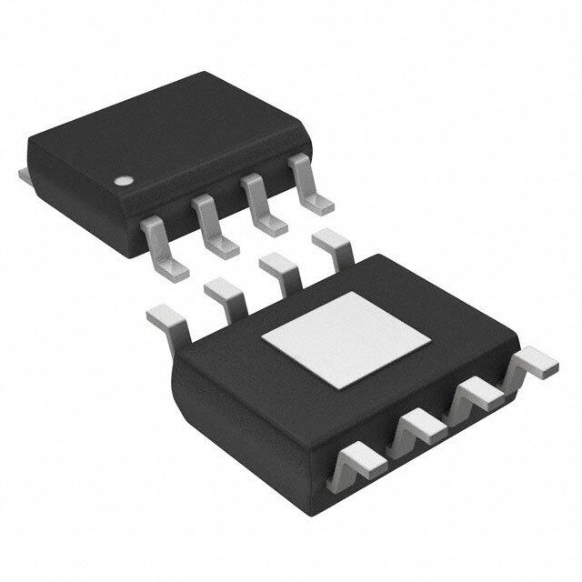
| 描述 | IC REG LDO ADJ 1A 10DFN低压差稳压器 SINGLE 1A ADJ VOUTLD 3X3 10LD W/ANN |
| 产品分类 | |
| 品牌 | Intersil |
| 产品手册 | |
| 产品图片 |
|
| rohs | 符合RoHS无铅 / 符合限制有害物质指令(RoHS)规范要求 |
| 产品系列 | 电源管理 IC,低压差稳压器,Intersil ISL80101IRAJZ-TK- |
| 数据手册 | |
| 产品型号 | ISL80101IRAJZ-TK |
| 产品培训模块 | http://www.digikey.cn/PTM/IndividualPTM.page?site=cn&lang=zhs&ptm=25476http://www.digikey.cn/PTM/IndividualPTM.page?site=cn&lang=zhs&ptm=25534 |
| 产品种类 | 低压差稳压器 |
| 供应商器件封装 | 10-DFN(3x3) |
| 其它名称 | ISL80101IRAJZ-TKCT |
| 包装 | 剪切带 (CT) |
| 商标 | Intersil |
| 回动电压—最大值 | 0.212 V at 1 A |
| 安装类型 | 表面贴装 |
| 安装风格 | SMD/SMT |
| 封装 | Reel |
| 封装/外壳 | 10-VFDFN 裸露焊盘 |
| 封装/箱体 | DFN EP |
| 工作温度 | -40°C ~ 125°C |
| 工厂包装数量 | 1000 |
| 最大工作温度 | + 125 C |
| 最大输入电压 | 6 V |
| 最小工作温度 | - 40 C |
| 最小输入电压 | 2.2 V |
| 标准包装 | 1 |
| 电压-跌落(典型值) | 0.13V @ 1A |
| 电压-输入 | 2.2 V ~ 6 V |
| 电压-输出 | 0.8 V ~ 5 V |
| 电压调节准确度 | +/- 0.2 % |
| 电流-输出 | 1A |
| 电流-限制(最小值) | 1.75A |
| 稳压器拓扑 | 正,可调式 |
| 稳压器数 | 1 |
| 系列 | ISL80101 |
| 线路调整率 | 1 % |
| 负载调节 | - 1 % |
| 输出电压 | 0.8 V to 5 V |
| 输出电流 | 3 A |
| 输出端数量 | 1 Output |
| 输出类型 | Adjustable |


- 商务部:美国ITC正式对集成电路等产品启动337调查
- 曝三星4nm工艺存在良率问题 高通将骁龙8 Gen1或转产台积电
- 太阳诱电将投资9.5亿元在常州建新厂生产MLCC 预计2023年完工
- 英特尔发布欧洲新工厂建设计划 深化IDM 2.0 战略
- 台积电先进制程称霸业界 有大客户加持明年业绩稳了
- 达到5530亿美元!SIA预计今年全球半导体销售额将创下新高
- 英特尔拟将自动驾驶子公司Mobileye上市 估值或超500亿美元
- 三星加码芯片和SET,合并消费电子和移动部门,撤换高东真等 CEO
- 三星电子宣布重大人事变动 还合并消费电子和移动部门
- 海关总署:前11个月进口集成电路产品价值2.52万亿元 增长14.8%


PDF Datasheet 数据手册内容提取
DATASHEET ISL80101-ADJ FN7834 High Performance 1A LDO Rev 3.00 August 26, 2015 The ISL80101-ADJ is a low voltage, high current, single output Features LDO specified at 1A output current. This LDO operates from input voltages from 2.2V to 6V, and is capable of providing • ±1.8% VOUT accuracy guaranteed over line, load and output voltages from 0.8V to 5V. The ISL80101-ADJ features TJ=-40°C to +125°C an adjustable output. For the fixed output version of the • Very low 130mV dropout voltage at VOUT = 2.5V ISL80101-ADJ, please refer to the ISL80101 datasheet. • Very fast transient response A submicron BiCMOS process is utilized for this product family • Programmable soft-starting to deliver the best in class analog performance and overall value. This CMOS LDO will consume significantly lower • Power-good output quiescent current as a function of load compared to bipolar • Excellent 65dB PSRR LDOs, which translates into higher efficiency and packages • Current limit protection with smaller footprints. State of the art internal compensation achieves a very fast load transient response. An external • Thermal shutdown function capacitor on the soft-start pin provides an adjustable • Available in a 10 Ld DFN package soft-starting ramp. The ENABLE feature allows the part to be • Pb-Free (RoHS compliant) placed into a low quiescent current shutdown mode. A Power-good logic output signals a fault condition. Applications Table1 shows the differences between the ISL80101-ADJ and • DSP, FPGA and µP core power supplies others in its family: • Noise-sensitive instrumentation systems TABLE 1. KEY DIFFERENCES BETWEEN FAMILY OF PARTS • Post regulation of switched mode power supplies PROGRAMMABLE ILIMIT ADJ OR FIXED • Industrial systems PART NUMBER ILIMIT (DEFAULT) VOUT ISL80101-ADJ No 1.75A ADJ • Medical equipment ISL80101 No 1.75A 1.8V, 2.5V, • Telecommunications and networking equipment 3.3V, 5.0V • Servers ISL80101A Yes 1.62A ADJ • Hard disk drives (HD/HDD) ISL80121-5 Yes 0.75A 5.0V Related Literature •AN1592, “ISL80101 High Performance 1A LDO Evaluation Board User Guide” 2.5V ± 10% 1.8V 140 10 1 VIN VOUT 10CµINF 9 VIN VOUT 282pF 2.61k 1C0OµUFT mV) 120 CPB R2 E ( 100 10k ADJ 3 100k AG R3 ISL80101-ADJ 1.00k RPG OLT 80 R1 T V 60 U 7 ENABLE PG 4 PO 40 O R D 6 20 VOUT = 2.5V SS 0.01µF GND 0 CSS 5 0 0.2 0.4 0.6 0.8 1.0 OUTPUT CURRENT (A) FIGURE 1. TYPICAL APPLICATION CIRCUIT FIGURE 2. DROPOUT vs LOAD CURRENT FN7834 Rev 3.00 Page 1 of 12 August 26, 2015
ISL80101-ADJ Block Diagram VIN EN CONTROL LOGIC - FET DRIVER EA WITH CURRENT REFERENCE + LIMIT TSHEENRSMOARL SOFT-+START VOUT PG SS + ADJ PG - GND Ordering Information PART NUMBER PART VOUT VOLTAGE TEMP RANGE PACKAGE (Notes3, 4) MARKING (Note2) (°C) (RoHS Compliant) PKG DWG. # ISL80101IRAJZ (Note1) DZAB ADJ -40 to +125 10 Ld 3x3 DFN L10.3x3 ISL80101EVAL2Z Evaluation Board NOTES: 1. Add “-T*” for Tape and Reel. Please refer to TB347 for details on reel specifications. 2. For other output voltages, contact Intersil Marketing. 3. These Intersil Pb-free plastic packaged products employ special Pb-free material sets, molding compounds/die attach materials, and 100% matte tin plate plus anneal (e3 termination finish, which is RoHS compliant and compatible with both SnPb and Pb-free soldering operations). Intersil Pb-free products are MSL classified at Pb-free peak reflow temperatures that meet or exceed the Pb-free requirements of IPC/JEDEC J STD-020. 4. For Moisture Sensitivity Level (MSL), please see product information page for ISL80101-ADJ. For more information on MSL please see techbrief TB363. FN7834 Rev 3.00 Page 2 of 12 August 26, 2015
ISL80101-ADJ Pin Configurations ISL80101-ADJ (10 LD 3x3 DFN) TOP VIEW VOUT 1 10 VIN VOUT 2 9 VIN ADJ 3 EPAD 8 NC PG 4 7 ENABLE GND 5 6 SS Pin Descriptions PIN NUMBER PIN NAME DESCRIPTION 1, 2 VOUT Regulated output voltage. A X5R/X7R output capacitor is required for stability. See “External Capacitor Requirements” on page8 for more details. 3 ADJ This pin is connected to the feedback resistor divider and provides voltage feedback signals for the LDO to set the output voltage. In addition, the PGOOD circuit uses this input to monitor the output voltage status. 4 PG This is an open-drain logic output used to indicate the status of the output voltage. Logic low indicates VOUT is not in regulation. Must be grounded if not used. 5 GND Ground 6 SS External capacitor on this pin adjusts start-up ramp and controls inrush current. 7 ENABLE VIN independent chip enable. TTL and CMOS compatible. 8 NC No connection; Leave floating. 9, 10 VIN Input supply; A minimum of 10µF X5R/X7R input capacitor is required for proper operation. See “External Capacitor Requirements” on page8 for more details. - EPAD EPAD at ground potential. It is recommended to solder the EPAD to the ground plane. FN7834 Rev 3.00 Page 3 of 12 August 26, 2015
ISL80101-ADJ Absolute Maximum Ratings Thermal Information VIN Relative to GND (Note5). . . . . . . . . . . . . . . . . . . . . . . . . . -0.3V to +6.5V Thermal Resistance (Typical) JA (°C/W) JC (°C/W) VOUT Relative to GND (Note5) . . . . . . . . . . . . . . . . . . . . . . . . -0.3V to +6.5V 10 Ld DFN Package (Notes6, 7) . . . . . . . . 48 7 PG, ENABLE, ADJ, SS Storage Temperature Range. . . . . . . . . . . . . . . . . . . . . . . .-65°C to +150°C Relative to GND (Note5). . . . . . . . . . . . . . . . . . . . . . . . . . . -0.3V to +6.5V Junction Temperature . . . . . . . . . . . . . . . . . . . . . . . . . . . . . . . . . . . . .+150°C ESD Rating Pb-Free Reflow Profile . . . . . . . . . . . . . . . . . . . . . . . . . . . . . . . . . . see TB493 Human Body Model (Tested per JESD22 A114F). . . . . . . . . . . . . . .2.5kV Charge Device Model (Tested per JESD22-C101C). . . . . . . . . . . . . . . 2kV Recommended Operating Conditions Latch-up (Tested per JESD78C, Class 2, Level A) . . . .±100mA at +125°C (Notes8, 9) Junction Temperature Range (TJ) (Note8) . . . . . . . . . . . .-40°C to +125°C VIN Relative to GND . . . . . . . . . . . . . . . . . . . . . . . . . . . . . . . . . . . . .2.2V to 6V VOUT Range. . . . . . . . . . . . . . . . . . . . . . . . . . . . . . . . . . . . . . . . . 800mV to 5V PG, ENABLE, ADJ, SS relative to GND . . . . . . . . . . . . . . . . . . . . . . . 0V to 6V PG Sink Current . . . . . . . . . . . . . . . . . . . . . . . . . . . . . . . . . . . . . . . . . . <10mA CAUTION: Do not operate at or near the maximum ratings listed for extended periods of time. Exposure to such conditions may adversely impact product reliability and result in failures not covered by warranty. NOTES: 5. ABS max voltage rating is defined as the voltage applied for a lifetime average duty cycle above 6V of 1%. 6. JA is measured in free air with the component mounted on a high effective thermal conductivity test board with “direct attach” features. See Tech Brief TB379. 7. For JC, the “case temp” location is the center of the exposed metal pad on the package underside. 8. Extended operation at these conditions may compromise reliability. Exceeding these limits will result in damage. Recommended operating conditions define limits where specifications are guaranteed. 9. Electromigration specification defined as lifetime average junction temperature of +110°C where max rated DCcurrent=lifetime average current. Electrical Specifications Unless otherwise noted, 2.2V < VIN < 6V, VOUT = 0.5V, TJ = +25°C. Applications must follow thermal guidelines of the package to determine worst case junction temperature. Please refer to “Applications Information” on page8 and Tech Brief TB379. Boldface limits apply across the operating temperature range, -40°C to +125°C. MIN MAX PARAMETER SYMBOL TEST CONDITIONS (Note10) TYP (Note10) UNITS DC CHARACTERISTICS Feedback Pin (ADJOptionOnly) VADJ VOUT + 0.4V < VIN < 6V, VOUT = 2.5V, 0A < ILOAD < 1A 491 500 509 mV DC Input Line Regulation (VOUT low line - VOUT + 0.4V < VIN < 6V, VOUT = 2.5V -1 1 % VOUT high line)/VOUT low line DC Output Load Regulation (VOUT no load- 0A < ILOAD < 1A, VOUT = 2.5V -1 1 % VOUT high load)/ VOUT no load Feedback Input Current VADJ = 0.5V 0.01 1 µA Ground Pin Current IQ ILOAD = 0A, VOUT + 0.4V < VIN < 6V, VOUT = 2.5V 3 5 mA ILOAD = 1A, VOUT + 0.4V < VIN < 6V, VOUT = 2.5V 5 7 mA Ground Pin Current in Shutdown ISHDN ENABLE Pin = 0.2V, VIN = 6V 0.2 12 µA Dropout Voltage (Note11) VDO ILOAD = 1A, VOUT = 2.5V 130 212 mV Output Short Circuit Current OCP VOUT = 0V 1.75 A Thermal Shutdown Temperature TSD 160 °C Thermal Shutdown Hysteresis TSDn 30 °C AC CHARACTERISTICS Input Supply Ripple Rejection PSRR f = 1kHz, ILOAD = 1A; VIN = 2.2V, VOUT = 1.8V 58 dB f = 120Hz, ILOAD = 1A; VIN = 2.2V, VOUT = 1.8V 65 dB Output Noise Voltage ILOAD = 1A, BW = 100Hz < f < 100kHz, VIN = 2.2V, 53 µVRMS VOUT = 1.8V FN7834 Rev 3.00 Page 4 of 12 August 26, 2015
ISL80101-ADJ Electrical Specifications Unless otherwise noted, 2.2V < VIN < 6V, VOUT = 0.5V, TJ = +25°C. Applications must follow thermal guidelines of the package to determine worst case junction temperature. Please refer to “Applications Information” on page8 and Tech Brief TB379. Boldface limits apply across the operating temperature range, -40°C to +125°C. (Continued) MIN MAX PARAMETER SYMBOL TEST CONDITIONS (Note10) TYP (Note10) UNITS ENABLE PIN CHARACTERISTICS Turn-on Threshold 0.5 0.8 1 V Hysteresis 10 80 200 mV ENABLE Pin Turn-on Delay COUT = 10µF, ILOAD = 1A 100 µs ENABLE Pin Leakage Current VIN = 6V, ENABLE = 2.8V 1 µA SOFT-START CHARACTERISTICS SS Pin Currents (Note12) IPD VIN = 3.5V, ENABLE = 0V, SS = 1V 0.5 1 1.3 mA ICHG -3.3 -2 -0.8 µA PG PIN CHARACTERISTICS VOUT PG Flag Threshold 75 85 92 %VOUT VOUT PG Flag Hysteresis 4 % PG Flag Low Voltage VIN = 3V, ISINK = 500µA 100 mV PG Flag Leakage Current VIN = 6V, PG = 6V 1 µA NOTES: 10. Compliance to datasheet limits is assured by one or more methods: production test, characterization and/or design. 11. Dropout is defined as the difference in supply VIN and VOUT when the supply produces a 2% drop in VOUT from its nominal voltage. 12. IPD is the internal pull down current that discharges the external SS capacitor on disable. ICHG is the current from the SS pin that charges the external SS capacitor during start-up. FN7834 Rev 3.00 Page 5 of 12 August 26, 2015
ISL80101-ADJ Typical Operating Performance Unless otherwise noted: VIN = 2.2V, VOUT = 1.8V, CIN = COUT = 10µF, TJ = +25°C, IL = 0A. 200 1.8 180 VOUT = 2.5V 1.2 V) 160 m E ( 140 IOUT = 1.0A 0.6 G A 120 %) OLT 100 (UT 0 UT V 80 IOUT = 0.5A VO O -0.6 P 60 RO IOUT = 0.1A D 40 -1.2 20 0 -1.8 -40 -25 -10 5 20 35 50 65 80 95 110 125 -50 -25 0 25 50 75 100 125 150 TEMPERATURE (°C) JUNCTION TEMPERATURE (°C) FIGURE 3. DROPOUT VOLTAGE vs TEMPERATURE FIGURE 4. VOUT vs TEMPERATURE 2.0 1.8 1.8 1.2 1.6 V) GE ( 1.4 0.6 +25°C A 1.2 %) OLT 1.0 +125°C (UT 0 V O TPUT 00..68 +25°C -40°C V -0.6 +125°C -40°C U O 0.4 -1.2 0.2 0 -1.8 0 1 2 3 4 5 6 0 0.25 0.50 0.75 1.00 SUPPLY VOLTAGE (V) OUTPUT CURRENT (A) FIGURE 5. OUTPUT VOLTAGE vs SUPPLY VOLTAGE FIGURE 6. OUTPUT VOLTAGE vs OUTPUT CURRENT 3.5 5 3.0 A) A) 4 m 2.5 m T ( T ( N N RE 2.0 RE 3 R R U U C 1.5 C ND +25°C +125°C -40°C ND 2 U U O 1.0 O R R G G 1 0.5 0 0 0 0.2 0.4 0.6 0.8 1.0 2 3 4 5 6 LOAD CURRENT (A) INPUT VOLTAGE (V) FIGURE 7. GROUND CURRENT vs LOAD CURRENT FIGURE 8. GROUND CURRENT vs SUPPLY VOLTAGE FN7834 Rev 3.00 Page 6 of 12 August 26, 2015
ISL80101-ADJ Typical Operating Performance Unless otherwise noted: VIN = 2.2V, VOUT = 1.8V, CIN = COUT = 10µF, TJ = +25°C, IL = 0A. (Continued) 3.5 2.5 2.0 VOLTAGE RAILS AT 50mV/DIV T (A) VIN = 6V EN 1.5 VIN = 2.2V R R U VIN = 3.7V, VOUT = 3.3V, COUT = 10µF, CPB = 100pF C 1.0 0.5 VIN = 2.9V, VOUT = 2.5V, COUT = 10µF, CPB = 82pF 0 -40 -25 -10 5 20 35 50 65 80 95 110 125 JUNCTION TEMPERATURE (°C) VIN = 2.5V, VOUT = 1.8V, COUT = 10µF, CPB = 82pF FIGURE 10. CURRENT LIMIT vs TEMPERATURE (VOUT = 0V) VIN = 2.5V, VOUT = 1.5V, COUT = 22µF, CPB = 150pF ENABLE (2V/DIV) VIN = 2.5V, VOUT = 1.2V, COUT = 47µF, CPB = 270pF VOUT (1V/DIV) VIN = 2.5V, VOUT = 1.0V, COUT = 47µF, CPB = 220pF SS (1V/DIV) 1A 1mA di/dt = 4A/µs PG (1V/DIV) (500µs/DIV) TIME (20µs/DIV) FIGURE 9. LOAD TRANSIENT RESPONSE FIGURE 11. ENABLE START-UP (CSS = 2.2nF) 90 90 80 500mA 80 COUT = 10µF, CPB = 82pF 70 1A 70 COUT = 100µF 60 60 B) B) d 50 100mA 0mA d 50 R ( R ( R 40 R 40 S S P P 30 30 20 20 10 10 CPB = 82pF 0 0 100 1k 10k 100k 1M 100 1k 10k 100k 1M FREQUENCY (Hz) FREQUENCY (Hz) FIGURE 12. PSRR vs FREQUENCY FOR VARIOUS LOAD CURRENTS FIGURE 13. PSRR vs FREQUENCY FOR VARIOUS OUTPUT CAPACITORS (IOUT= 100mA) FN7834 Rev 3.00 Page 7 of 12 August 26, 2015
ISL80101-ADJ Typical Operating Performance Unless otherwise noted: VIN = 2.2V, VOUT = 1.8V, CIN = COUT = 10µF, TJ = +25°C, IL = 0A. (Continued) 10 VIN = 3.8V VIN = 2.25V VIN (2V/DIV) z) 1 H √ V/ µ E ( S OI N 0.1 VIN = 2.2V VOUT = 1.8 VOUT (5mV/DIV) COUT = 10µF IOUT = 1A 0.01 10 100 1k 10k 100k TIME (200µs/DIV) FREQUENCY (Hz) FIGURE 14. LINE TRANSIENT RESPONSE FIGURE 15. OUTPUT NOISE SPECTRAL DENSITY Applications Information C x0.5 T = -----S----S--------------- (EQ. 1) start 2A Input Voltage Requirements Equation2 determines the CSS required for a specific start-up ISL80101-ADJ is capable of delivering output voltages from 0.8V in-rush current, where VOUT is the output voltage, COUT is the to 5.0V. Due to the nature of an LDO, VIN must be some margin total capacitance on the output and IINRUSH is the desired in-rush higher than VOUT plus dropout at the maximum rated current of current. tVhOeU Ta.p Tphliec avteiroyn l oifw a cdtriovpeo fuiltte srpinegc i(fPicSaRtiRon) ios fe txhpies cftaemd iflyro omf LVDINO sto CSS = V-----O-I---U----T----x----C----O-----U-x---T0---x-.-5--2--V------A--- (EQ. 2) INRUSH allows applications to design for a level of efficiency that can accommodate profiles smaller than the TO220/263. The external capacitor is always discharged to ground at the beginning of start-up or enabling. Enable Operation Output Voltage Selection The Enable turn-on threshold is typically 800mV with 80mV of hysteresis. This pin must not be left floating, and should be tied An external resistor divider, R1 and R2 as referenced in Figure1 to VIN if not used. A 1kΩ to 10kΩ pull-up resistor is required for on page1, is used to scale the output voltage relative to the applications that use open collector or open-drain outputs to internal reference voltage. The output voltage can be control the Enable pin. An internal pull-up or pull-down resistor to programmed to any level between 0.8V and 5V. The change these values is available upon request. The Enable pin recommended value for R2 is 500Ω to 5kΩ. R1 is then chosen to may be connected directly to VIN for applications with outputs satisfy Equation3. that are always on. V = 0.5VR-----2--+1 (EQ. 3) Power-Good Operation OUT R1 PG is a logic output that indicates the status of VOUT. The PG flag External Capacitor Requirements is an open-drain NMOS that can sink up to 10mA. It requires an External capacitors are required for proper operation. Careful external pull-up resistor typically connected to the VOUT pin. The attention must be paid to the layout guidelines and selection of PG pin should not be pulled up to a voltage source greater than capacitor type and value to ensure optimal performance. VIN. PG goes low when the output voltage drops below 84% of the nominal output voltage or if the part is disabled. The PG comparator OUTPUT CAPACITOR functions during current limit and thermal shutdown. For applications The ISL80101-ADJ applies state-of-the-art internal compensation not using this feature, connect this pin to ground. to keep the selection of the output capacitor simple for the Soft-Start Operation customer. Stable operation over full temperature, VIN range, VOUT range and load extremes are guaranteed for all capacitor The soft-start circuit controls the rate at which the output voltage types and values assuming the minimum recommended ceramic rises up to regulation at power-up or LDO enable. This start-up capacitor is used for local bypass on VOUT. There is a growing ramp time can be set by adding an external capacitor from the trend to use very-low ESR multilayer ceramic capacitors (MLCC) SS pin to ground. An internal 2µA current source charges up this because they can support fast load transients and also bypass CSS and the feedback reference voltage is clamped to the very high frequency noise from other sources. However, the voltage across it. The start-up time is set by Equation1. effective capacitance of MLCCs drops with applied voltage, age, FN7834 Rev 3.00 Page 8 of 12 August 26, 2015
ISL80101-ADJ and temperature. X7R and X5R dielectric ceramic capacitors are Power Dissipation and Thermals strongly recommended as they typically maintain a capacitance The junction temperature must not exceed the range specified in range within ±20% of nominal voltage over full operating ratings the “Recommended Operating Conditions” on page4. The power of temperature and voltage. This output capacitor must be dissipation can be calculated by using Equation5: connected to the VOUT and GND pins of the LDO with PCB traces no longer than 0.5cm. P = V –V I +V I (EQ. 5) D IN OUT OUT IN GND Additional capacitors of any value in ceramic, POSCAP, alum/tantalum electrolytic types may be placed in parallel to The maximum allowable junction temperature, TJ(MAX) and the improve PSRR at higher frequencies and/or load transient AC maximum expected ambient temperature, TA(MAX) determine the output voltage tolerances. The use of CPB (see following section) maximum allowable power dissipation, as shown in Equation6: is recommended when only the minimum recommended P = T –T (EQ. 6) DMAX JMAX A JA ceramic capacitor is used on the output. Please refer to Table2 for these minimum conditions for various output voltages. JA is the junction-to-ambient thermal resistance. For safe operation, ensure that the power dissipation PD, Phase Boost Capacitor calculated from Equation5, is less than the maximum allowable A small phase boost capacitor, CPB, can be placed across the top power dissipation PD(MAX). resistor, R2, in the feedback resistor divider network in order to The DFN package uses the copper area on the PCB as a heatsink. place a zero at: The EPAD of this package must be soldered to the copper plane F = ----------------1------------------ (EQ. 4) (GND plane) for effective heat dissipation. Figure16 shows a curve z 2xR2xCPB for the JA of the DFN package for different copper area sizes. This zero increases the crossover frequency of the LDO and 49 provides additional phase resulting in faster load transient 47 response. It is important to note that LDO stability and load transient 45 performance are affected by the type of output capacitor used. W For optimal result, empirical tuning of CPB is suggested for each °C/A 43 specific application. It is recommended to not use CPB when high J ESR capacitors such as Aluminum Electrolytic or Tantalum are 41 used on the output. 39 Table2 shows the recommended minimum ceramic COUT and corresponding CPB, R2 and R1 for different output voltages. 37 2 4 6 8 10 12 14 16 18 20 22 24 TABLE 2. RECOMMENDED CPB FOR DIFFERENT VOUT AND COUT EPAD-MOUNT COPPER LAND AREA ON PCB, mm2 FIGURE 16. 3mmx3mm 10-PIN DFN ON 4-LAYER PCB WITH VOUT R2 R1 COUT CPB (V) (kΩ) (kΩ) (µF) (pF) THERMAL VIAS JA vs EPAD-MOUNT COPPER LAND AREA ON PCB 5.0 2.61 0.287 10 100 Thermal Fault Protection 3.3 2.61 0.464 10 100 2.5 2.61 0.649 10 82 The power level and the thermal impedance of the package (+45°C/W for DFN) determine when the junction temperature 1.8 2.61 1.0 10 82 exceeds the thermal shutdown temperature. In the event that the 1.5 2.61 1.3 10 68 die temperature exceeds around +160°C, the output of the LDO will shut down until the die temperature cools down to about +130°C. 1.5 2.61 1.3 22 150 Current Limit Protection 1.2 2.61 1.87 22 120 The ISL80101-ADJ LDO incorporates protection against overcurrent 1.2 2.61 1.87 47 270 due to any short or overload condition applied to the output pin. The 1.0 2.61 2.61 47 220 LDO performs as a constant current source when the output current exceeds the current limit threshold noted in the “Electrical 0.8 2.61 4.32 47 220 Specifications” table on page4. If the short or overload condition is INPUT CAPACITOR removed from VOUT, then the output returns to normal voltage regulation mode. In the event of an overload condition, the LDO may For proper operation, a minimum capacitance of 10µF X5R/X7R begin to cycle on and off due to the die temperature exceeding is required at the input. This ceramic input capacitor must be thermal fault condition and subsequently cooling down after the connected to the VIN and GND pins of the LDO with PCB traces no power device is turned off. longer than 0.5cm. FN7834 Rev 3.00 Page 9 of 12 August 26, 2015
ISL80101-ADJ Revision History The revision history provided is for informational purposes only and is believed to be accurate, but not warranted. Please go to web to make sure you have the latest revision. DATE REVISION CHANGE August 26, 2015 FN7834.3 Added Related Literature to page 1. Removed 1st bullet in Features on page 1 which read ±0.2% initial VOUT accuracy. Changed 7th bullet in Features on page 1 from Excellent 58dB PSRR at 1kHz to Excellent 65dB PSRR Updated the EA amp in the “Block Diagram” on page2 by switching the + and - terminals. The positive terminal is now connected to the ADJ pin. Removed “SENSE” pin Reference in diagram “Pin Descriptions” on page3 - Removed “minimum 10µF” from 1st sentence in VOUT description. “Absolute Maximum Ratings” on page4 - Removed Machine Model and changed latch up from +85°C to +125°C. Removed "SENSE" from “ADJ” in "‘Recommended Operating Conditions" on page4. Added “VIN =” to values in Figure10 on page7 Changed Title of Figure3 on page6 from Dropout vs Temperature to Dropout Voltage vs Temperature Changed Title in Figure12 on page7 from PSRR vs Frequency and Load Current to PSRR vs Frequency for various load currents Changed Title in Figure13 on page7 from PSRR vs Frequency and Output Capacitance (IOUT = 100mA) to PSRR vs Frequency for various output capacitors (IOUT=100mA) Electrical Spec changes: Electrical Spec Table conditions on page4 changed: VIN = VOUT + 0.4V, VOUT = 1.8V, CIN = COUT = 2.2µF, to: 2.2V < VIN < 6V, VOUT = 0.5V “Feedback Pin (ADJOptionOnly)” Test Conditions changed from: 2.2V VIN 6V, 0A < ILOAD < 1A to: VOUT + 0.4V < VIN < 6V, VOUT = 2.5V, 0A < ILOAD < 1A "DC Input Line Regulation" on page 4 - changed symbol from VOUT/VIN to VOUT low line - VOUT high line)/VOUT low line and added MIN -1. Test Conditions changed from: VOUT + 0.5V < VIN < 5V to: VOUT + 0.4V < VIN < 6V, VOUT = 2.5V “DC Output Load Regulation” on page4 - changed symbol from VOUT/IOUT to VOUT no load-VOUT high load)/ VOUT no load and added MAX 1. Test Conditions changed from: 0A < ILOAD < 1A, All voltage options to: 0A < ILOAD < 1A, VOUT = 2.5V Ground Pin Current Test Conditions changed from: ILOAD = 0A, 2.2V < VIN < 6V to: ILOAD = 0A, VOUT + 0.4V < VIN < 6V, VOUT = 2.5V ILOAD = 1A, 2.2V < VIN < 6V to: ILOAD = 1A, VOUT + 0.4V < VIN < 6V, VOUT = 2.5V Output Short Circuit Current Test Conditions changed from: VOUT = 0V, 2.2V < VIN < 6V to: VOUT = 0V Thermal Shutdown Temperature, Thermal Shutdown Hysteresis, Turn-on Threshold and Hysteresis - Removed Test Conditions Removed “Rising Threshold” from ““Thermal Shutdown Hysteresis” on page4 and from “Hysteresis” on page5 “AC CHARACTERISTICS” on page4 in PSRR - changed TYP from "72" to "65" for f = 120Hz. Added to Test Conditions: VOUT = 1.8V Output Noise Voltage in test conditions changed “10Hz” to “100Hz”, added VIN = 2.2V, VOUT = 1.8V. Changed TYP from “63” to “53” “PG Flag Low Voltage” on page5 changed in test conditions - VIN = 2.5V TO VIN = 3V “Turn-on Threshold” on page5 changed MIN from: 0.3; to: 0.5 “Hysteresis” on page5 changed in test conditions from: 2.2V < VOUT + 0.4V < 6V, to: 2.2V < VIN < 6V “ENABLE Pin Leakage Current” on page5 changed “Enable = 3V” to “Enable = 2.8V” ------------------------------------------------- Updated Output Spectral Noise Density (Figure15 on page8) and changed IL = 1A to IOUT = 1A Updated POD L10.3x3 to most recent revision with changes as follows: Added missing dimension 0.415 in Typical Recommended land pattern. Shortened the e-pad rectangle on both the recommended land pattern and the package bottom view to line up with the centers of the corner pins. Tiebar Note 4 updated From: Tiebar shown (if present) is a non-functional feature. To: Tiebar shown (if present) is a non-functional feature and may be located on any of the 4 sides (or ends). FN7834 Rev 3.00 Page 10 of 12 August 26, 2015
ISL80101-ADJ Revision History The revision history provided is for informational purposes only and is believed to be accurate, but not warranted. Please go to web to make sure you have the latest revision. (Continued) DATE REVISION CHANGE July 31, 2014 FN7834.2 Updated the “Block Diagram” on page2 reversed the + and - terminals on the EA amp. The inverting terminal is now connected to the Adj/Sense pin. Updated About Intersil verbiage to new standard. Updated “Package Outline Drawing” on page12 to latest revision. August 3, 2011 FN7834.1 PAGE 1 1. Introduction, paragraph 1: Last two sentences removed, and replaced with: "The ISL80101-ADJ features an adjustable output. For the fixed output version of the ISL80101, please refer to the ISL80101 datasheet." 2. Table 1: Replaced Table 1 with Table 1 from FN6931 to include the "ADJ or Fixed VOUT" column and "ISL80101-ADJ" row. 3. Features: "Available in a 10 Ld DFN Package" has "TO220-5, TO263-5 and SOT223-5 to follow soon" removed. PAGE 5 1. Enable Pin Characteristics a. "Enable Pin Turn-on Delay" changed to "ENABLE Pin Turn-on Delay" b. "Enable Pin Leakage Current" changed to "ENABLE Pin Leakage Current" PAGE 7 Figure 9: Timescale changed from "20µs/DIV" to "TIME (20µs/DIV)" PAGE 8 2. Equation 1 - Parentheses deleted. 3. Equation 2 - Parentheses deleted. March 31, 2011 FN7834.0 Initial Release. About Intersil Intersil Corporation is a leading provider of innovative power management and precision analog solutions. The company's products address some of the largest markets within the industrial and infrastructure, mobile computing and high-end consumer markets. For the most updated datasheet, application notes, related documentation and related parts, please see the respective product information page found at www.intersil.com. You may report errors or suggestions for improving this datasheet by visiting www.intersil.com/ask. Reliability reports are also available from our website at www.intersil.com/support. © Copyright Intersil Americas LLC 2011-2015. All Rights Reserved. All trademarks and registered trademarks are the property of their respective owners. For additional products, see www.intersil.com/en/products.html Intersil products are manufactured, assembled and tested utilizing ISO9001 quality systems as noted in the quality certifications found at www.intersil.com/en/support/qualandreliability.html Intersil products are sold by description only. Intersil may modify the circuit design and/or specifications of products at any time without notice, provided that such modification does not, in Intersil's sole judgment, affect the form, fit or function of the product. Accordingly, the reader is cautioned to verify that datasheets are current before placing orders. Information furnished by Intersil is believed to be accurate and reliable. However, no responsibility is assumed by Intersil or its subsidiaries for its use; nor for any infringements of patents or other rights of third parties which may result from its use. No license is granted by implication or otherwise under any patent or patent rights of Intersil or its subsidiaries. For information regarding Intersil Corporation and its products, see www.intersil.com FN7834 Rev 3.00 Page 11 of 12 August 26, 2015
ISL80101-ADJ Package Outline Drawing L10.3x3 10 LEAD DUAL FLAT PACKAGE (DFN) Rev 11, 3/15 5 3.00 A PIN #1 INDEX AREA B 1 5 2 PIN 1 INDEX AREA 0 3.00 2.00.50 x 8 10 x 0.23 (4X) 0.10 1.60 10x 0.35 TOP VIEW BOTTOM VIEW (4X) 0.10 M CAB 0.415 0.23 0 .2 0 0 0.35 (10 x 0.55) SEE DETAIL "X" (10x 0.23) 0.10C 1.00MAX BASE PLANE C 0.20 SEATING PLANE 00 0.08C 2. SIDE VIEW (8x 0.50) 0.415 C 0.20 REF 4 1.60 0.05 2.85 TYP DETAIL "X" TYPICAL RECOMMENDED LAND PATTERN NOTES: 1. Dimensions are in millimeters. Dimensions in ( ) for Reference Only. 2. Dimensioning and tolerancing conform to ASME Y14.5m-1994. 3. Unless otherwise specified, tolerance : Decimal ± 0.05 4. Tiebar shown (if present) is a non-functional feature and may be located on any of the 4 sides (or ends). 5. The configuration of the pin #1 identifier is optional, but must be located within the zone indicated. The pin #1 identifier may be either a mold or mark feature. FN7834 Rev 3.00 Page 12 of 12 August 26, 2015