ICGOO在线商城 > 集成电路(IC) > PMIC - 稳压器 - 专用型 > ISL6363CRTZ
 Datasheet下载
- 型号: ISL6363CRTZ
- 制造商: Intersil
- 库位|库存: xxxx|xxxx
- 要求:
| 数量阶梯 | 香港交货 | 国内含税 |
| +xxxx | $xxxx | ¥xxxx |
查看当月历史价格
查看今年历史价格
ISL6363CRTZ产品简介:
ICGOO电子元器件商城为您提供ISL6363CRTZ由Intersil设计生产,在icgoo商城现货销售,并且可以通过原厂、代理商等渠道进行代购。 ISL6363CRTZ价格参考。IntersilISL6363CRTZ封装/规格:PMIC - 稳压器 - 专用型, - Controller, Intel VR12 Voltage Regulator IC 2 Output 48-TQFN (6x6)。您可以下载ISL6363CRTZ参考资料、Datasheet数据手册功能说明书,资料中有ISL6363CRTZ 详细功能的应用电路图电压和使用方法及教程。
ISL6363CRTZ是由Renesas Electronics America Inc.生产的一款专用型PMIC(电源管理集成电路),主要用于稳压器应用。该器件特别适用于需要高效、紧凑和高性能电源管理解决方案的场景,如笔记本电脑、平板电脑、服务器和其他便携式电子设备。

 主要应用场景:

1. 笔记本电脑和平板电脑:
   ISL6363CRTZ能够为这些设备提供高效的电源管理,确保系统在不同工作模式下的稳定性和性能。它支持多相位输出,可以为CPU、GPU等高功耗组件提供稳定的电流供应,同时减少发热和提高能效。

2. 服务器和数据中心:
   在服务器环境中,ISL6363CRTZ可以用于为处理器、内存和其他关键组件供电。其高效的电源转换能力有助于降低能耗,提升系统的整体性能和可靠性。此外,它还支持远程监控和故障诊断功能,便于维护和管理。

3. 便携式电子设备:
   对于智能手机、智能手表等便携式设备,ISL6363CRTZ能够提供高效的电源管理,延长电池寿命,同时确保设备在高负载下的稳定运行。其低功耗设计和快速响应特性非常适合这些对功耗敏感的应用。

4. 嵌入式系统:
   在工业自动化、物联网(IoT)设备等领域,ISL6363CRTZ可以为微控制器、传感器和其他外围设备提供稳定的电源供应。其灵活的配置选项和广泛的输入电压范围使其适用于多种嵌入式应用场景。

5. 汽车电子:
   在汽车电子系统中,ISL6363CRTZ可以用于为车载信息娱乐系统、ADAS(高级驾驶辅助系统)等提供可靠的电源管理。其宽泛的工作温度范围和抗干扰能力强的特点,使其能够在严苛的汽车环境中稳定工作。

总之,ISL6363CRTZ凭借其高效、紧凑和高性能的特点,广泛应用于各种需要稳定电源管理的领域,特别是在便携式设备、服务器和嵌入式系统中表现出色。
| 参数 | 数值 |
| 产品目录 | 集成电路 (IC) |
| 描述 | IC CONTROLLER VR12 48TQFN |
| 产品分类 | |
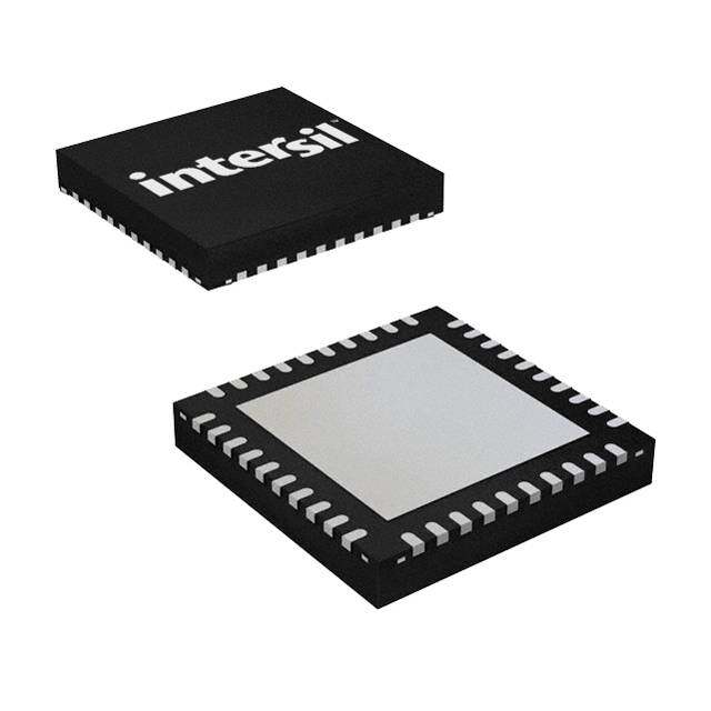
| 品牌 | Intersil |
| 数据手册 | |
| 产品图片 |
|
| 产品型号 | ISL6363CRTZ |
| PCN组件/产地 | |
| rohs | 无铅 / 符合限制有害物质指令(RoHS)规范要求 |
| 产品系列 | - |
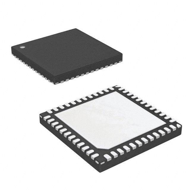
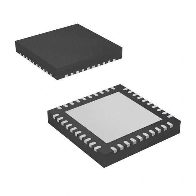
| 供应商器件封装 | 48-TQFN-EP(6x6) |
| 包装 | 管件 |
| 安装类型 | 表面贴装 |
| 封装/外壳 | 48-WFQFN 裸露焊盘 |
| 工作温度 | 0°C ~ 70°C |
| 应用 | 控制器,Intel VR12 |
| 标准包装 | 50 |
| 电压-输入 | 5 V ~ 12 V |
| 电压-输出 | 0.25 V ~ 1.52 V |
| 输出数 | 2 |


- 商务部:美国ITC正式对集成电路等产品启动337调查
- 曝三星4nm工艺存在良率问题 高通将骁龙8 Gen1或转产台积电
- 太阳诱电将投资9.5亿元在常州建新厂生产MLCC 预计2023年完工
- 英特尔发布欧洲新工厂建设计划 深化IDM 2.0 战略
- 台积电先进制程称霸业界 有大客户加持明年业绩稳了
- 达到5530亿美元!SIA预计今年全球半导体销售额将创下新高
- 英特尔拟将自动驾驶子公司Mobileye上市 估值或超500亿美元
- 三星加码芯片和SET,合并消费电子和移动部门,撤换高东真等 CEO
- 三星电子宣布重大人事变动 还合并消费电子和移动部门
- 海关总署:前11个月进口集成电路产品价值2.52万亿元 增长14.8%


PDF Datasheet 数据手册内容提取
IMSuLlti6p3ha6s3e PWM Regulator for VR12™N1c O-oD8NnT8eOt 8sRa -RkcIENttECo ToCpOEuO MCrR MTSMPeMIUELcEN hsoNnDrDi EcwEaDwDl FwS ROu.iEnpRPtp eNLorEArstiWC lC.Ec eDoMnEmEtSe/NtrIsG TacNtS DATASHERFeNEv6 18.T9080 Sep 5, 2013 Fully compliant with VR12™ specifications, the ISL6363 Features provides a complete solution for microprocessor core and graphics power supplies. It provides two Voltage Regulators • Serial Data Bus (SVID) (VRs) with three integrated gate drivers. The first output (VR1) • Dual Outputs: can be configured as a 4, 3, 2 or 1-phase VR while the second - Configurable 4, 3, 2 or 1-phase for the 1st Output with 2 output (VR2) is a 1-phase VR. The two VRs share a serial control Integrated Gate Drivers bus to communicate with the CPU and achieve lower cost and - 1-phase for the 2nd Output with Integrated Gate Driver smaller board area compared with a two-chip approach. • Precision Core Voltage Regulation Based on Intersil’s Robust Ripple Regulator R3 Technology™, - 0.5% System Accuracy Over-Temperature the PWM modulator, compared to traditional modulators, has faster transient settling time, variable switching frequency - Enhanced Load Line Accuracy during load transients and has improved light load efficiency • PS2 Compensation and High Frequency Load Transient with its ability to automatically change switching frequency. Compensation The ISL6363 has several other key features. Both outputs • Differential Remote Voltage Sensing support DCR current sensing with a single NTC thermistor for • Lossless Inductor DCR Current Sensing DCR temperature compensation or accurate resistor current sensing. Both outputs come with remote voltage sensing, • Programmable VBOOT Voltage at Start-up programmable VBOOT voltage, serial bus address, IMAX, TMAX, • Resistor Programmable Address, IMAX, TMAX for Both adjustable switching frequency, OC protection and separate Outputs power-good indicators. To reduce output capacitors, the • Adaptive Body Diode Conduction Time Reduction ISL6363 also has an additional compensation function for PS1/2 mode and high frequency load transient compensation. Applications • VR12 Desktop Computers Related Literature • ISL6363EVAL1Z User Guide 1.15 1.10 1.7mΩ LOADLINE VCORE 50mV/DIV V) 1.05 (RE 1.1V - PS1 O C V 1.00 1.1V - PS0 COMP 0.95 1V/DIV 65A STEP LOAD 0.90 1V/DIV 0 5 10 15 20 25 30 35 40 45 50 55 60 65 70 75 80 85 2µs/DIV IOUT (A) FIGURE 1. FAST TRANSIENT RESPONSE FIGURE 2. ACCURATE LOADLINE, VCORE vs IOUT FN6898 Rev 1.00 Page 1 of 32 Sep 5, 2013
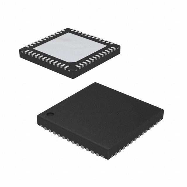
ISL6363 Ordering Information PART NUMBER TEMP. RANGE PACKAGE PKG. (Notes 1, 2, 3) PART MARKING (°C) (Pb-Free) DWG. # ISL6363CRTZ ISL6363 CRTZ 0 to +70 48 Ld 6x6 TQFN L48.6x6 ISL6363IRTZ ISL6363 IRTZ -40 to +85 48 Ld 6x6 TQFN L48.6x6 NOTES: 1. Add “-T*” suffix for tape and reel. Please refer to TB347 for details on reel specifications. 2. These Intersil Pb-free plastic packaged products employ special Pb-free material sets, molding compounds/die attach materials, and 100% matte tin plate plus anneal (e3 termination finish, which is RoHS compliant and compatible with both SnPb and Pb-free soldering operations). Intersil Pb-free products are MSL classified at Pb-free peak reflow temperatures that meet or exceed the Pb-free requirements of IPC/JEDEC J STD-020. 3. For Moisture Sensitivity Level (MSL), please see device information page for ISL6363. For more information on MSL please see techbrief TB363. Pin Configuration ISL6363 (48 LD TQFN) TOP VIEW DDR HASE1 GATE1 OOT1 GATE1 VCC GATE2 OOT2 GATE2 HASE2 WM3 WM4 A P U B L P L B U P P P 48 47 46 45 44 43 42 41 40 39 38 37 SCOMP 1 36PHASEG Temporary Pinout PGOOD 2 35UGATEG VCC 3 34BOOTG Subject to Change ISUMP 4 33LGATEG ISUMN 5 32PVCCG GND PAD ISEN1 6 31VR_HOT# (BOTTOM) ISEN2 7 30NTCG ISEN3 8 29ISUMNG ISEN4 9 28ISUMPG VSEN10 27RTNG PSICOMP11 26FBG RTN12 25COMPG 13 14 15 16 17 18 19 20 21 22 23 24 B P W C N N A # K G G G F COM V NT IMO VR_O SD ALERT SCL GOOD IMON VW P Pin Descriptions ISL6363 SYMBOL DESCRIPTION Bottom GND Common ground signal of the IC. Unless otherwise stated, signals are referenced to the GND pin. The pad should also be Pad used as the thermal pad for heat dissipation. 1 SCOMP This pin is a placeholder for potential future functionality. This pin can be left floating. 2 PGOOD Power-good open-drain output indicating when VR1 is able to supply a regulated voltage. Pull-up externally with a 680Ω resistor to +5V or 1kΩ to +3.3V. 3 VCC +5V bias supply pin. Connect a high quality 0.1µF capacitor from this pin to GND and place it as close to the pin as possible. A small resistor (2.2Ω for example) between the +5V supply and the decoupling capacitor is recommended. 4, 5 ISUMP, VR1 current sense input pins for current monitoring, droop current and overcurrent detection. ISUMN 6 ISEN1 VR1 phase 1 current sense input pin for phase current balancing. 7 ISEN2 VR1 phase 2 current sense input pin for phase current balancing. 8 ISEN3 VR1 phase 3 current sense input pin for phase current balancing. FN6898 Rev 1.00 Page 2 of 32 Sep 5, 2013
ISL6363 Pin Descriptions (Continued) ISL6363 SYMBOL DESCRIPTION 9 ISEN4 VR1 phase 4 current sense input pin for phase current balancing. 10 VSEN VR1 remote core voltage sense input. 11 PSICOMP This pin is used for improving transient response in PS2/3 mode of VR1 by switching in an additional type 3 compensation network to improve system gain and phase margin. Connect a resistor and capacitor from this pin to the output of VR1 near the feedback compensation network. 12 RTN VR1 remote voltage sensing return input. Connect this pin to the remote ground sensing location. 13 FB Inverting input of the error amplifier for VR1. 14 COMP This is a dual function pin. This pin is the output of the error amplifier for VR1. A resistor connected from this pin to GND programs IMAX for VR1 and VBOOT for both VR1 and VR2. Refer to Table 7 on page28. 15 VW A resistor from this pin to COMP programs the PWM switching frequency for VR1. 16 NTC One of the thermistor network inputs to the thermal monitoring circuit used to control the VR_HOT# signal. Use this pin to monitor the temperature of VR1. Place the NTC close to the desired thermal detection point on the PCB. 17 IMON Current monitoring output pin for VR1. The current sense signal from ISUMN and ISUMP is output on this pin to generate a voltage proportional to the output current of VR1. 18 VR_ON Enable input signal for the controller. A high level logic signal on this pin enables the controller and initiates soft-start for VR1 and VR2. 19, 20, 21 SDA, Data, alert and clock signal for the SVID communication bus between the CPU and VR1 and VR2. ALERT#, SCLK 22 PGOODG Power-good open-drain output indicating when VR2 is able to supply a regulated voltage. Pull-up externally with a 680Ω resistor to +5V or 1.0kΩ to 3.3V. 23 IMONG Current monitoring output pin for VR2. The current sense signal from ISUMNG and ISUMPG is output on this pin to generate a voltage proportional to the output current of VR2. 24 VWG A resistor from this pin to COMPG programs the PWM switching frequency for VR1. 25 COMPG This is a dual function pin. This pin is the output of the error amplifier for VR2. A resistor connected from this pin to GND programs IMAX for VR2 and TMAX for both VR1 and VR2. Refer to Table 8 on page28. 26 FBG Inverting input of the error amplifier for VR2. 27 RTNG VR2 remote voltage sensing return input. Connect this pin to the remote ground sensing location. 28, 29 ISUMPG, VR2 current sense input pin for current monitoring, droop current and overcurrent detection. ISUMNG 30 NTCG One of the thermistor network inputs to the thermal monitoring circuit used to control the VR_HOT# signal. Use this pin to monitor the temperature of VR2. Place the NTC close to the desired thermal detection point on the PCB. 31 VR_HOT# Open drain thermal overload output indicator. 32 PVCCG Input voltage bias for the internal gate driver for VR2. Connect +12V to this pin. Decouple with at least a 1µF MLCC capacitor and place it as close to the pin as possible. 33 LGATEG Output of the VR2 low-side MOSFET gate driver. Connect this pin to the gate of the VR2 low-side MOSFET. 34 BOOTG Connect a MLCC capacitor from this pin to the PHASEG pin. The boot capacitor is charged through an internal boot diode connected from the PVCCG pin to the BOOTG pin. 35 UGATEG Output of the VR2 high-side MOSFET gate drive. Connect this pin to the gate of the VR2 high-side MOSFET. 36 PHASEG Current return path for the VR2 high-side MOSFET gate driver. Connect this pin to the node connecting the source of the high-side MOSFET, the drain of the low-side MOSFET and the output inductor of VR2. 37 PWM4 PWM output for phase 4 of VR1. When PWM4 is pulled to +5V VCC, the controller will disable phase 4 of VR1. 38 PWM3 PWM output for phase 3 of VR1. When PWM3 is pulled to +5V VCC, the controller will disable phase 3 of VR1. 39 PHASE2 Current return path for the VR1 phase 2 high-side MOSFET gate driver. Connect this pin to the node connecting the source of the high-side MOSFET, the drain of the low-side MOSFET and the output inductor of phase 2. 40 UGATE2 Output of the VR1 phase 2 high-side MOSFET gate drive. Connect this pin to the gate of the high-side MOSFET of phase2. FN6898 Rev 1.00 Page 3 of 32 Sep 5, 2013
ISL6363 Pin Descriptions (Continued) ISL6363 SYMBOL DESCRIPTION 41 BOOT2 Connect an MLCC capacitor from this pin to the PHASE2 pin. The boot capacitor is charged through an internal boot diode connected from the PVCCG pin to the BOOTG pin. 42 LGATE2 Output of the VR1 phase 2 low-side MOSFET gate driver. Connect this pin to the gate of the low-side MOSFET of phase 2. 43 PVCC Input voltage bias for the internal gate drivers for VR1. Connect +12V to this pin. Decouple with at least a 1µF MLCC capacitor and place it as close to the pin as possible. 44 LGATE1 Output of the VR1 phase 1 low-side MOSFET gate driver. Connect this pin to the gate of the low-side MOSFET of phase 1. 45 BOOT1 Connect an MLCC capacitor from this pin to the PHASE1 pin. The boot capacitor is charged through an internal boot diode connected from the PVCC pin to the BOOT1 pin. 46 UGATE1 Output of the VR1 phase 1 high-side MOSFET gate drive. Connect this pin to the gate of the high-side MOSFET of phase1. 47 PHASE1 Current return path for the VR1 phase 1 high-side MOSFET gate driver. Connect this pin to the node connecting the source of the high-side MOSFET, the drain of the low-side MOSFET and the output inductor of phase 1. 48 ADDR A resistor from this pin to GND programs the SVID address for VR1 and VR2. Refer to Table 9 on page28. FN6898 Rev 1.00 Page 4 of 32 Sep 5, 2013
ISL6363 Block Diagram VWG COMPG COMPG + + RTNG + E/A BOOTG FBG _ VR2 MODULATOR DRIVER UGATEG IDROOPG PHASEG ISUMPG + CURRENT _ SENSE ISUMNG DRIVER LGATEG PGOODG IMONG OC FAULT OV FAULT NTCG TEMP T_MONITOR VCC NTC MONITOR VR_HOT# PVCCG ADDR IMAX COMPG PVCC VBOOT COMP TMAX SET (A/D) ADDR IMONG SCOMP VR_ON A/D IMON PWM4 DAC2 SDA DIGITAL D/A DAC1 PWM3 INTERFACE ALERT# MODE2 MODE MODE1 BOOT2 SCLK VREADY DRIVER UGATE2 VW PHASE2 COMP COMP + RTN + + VR1 DRIVER LGATE2 MODULATOR E/A _ FB PSICOMP BOOT1 CIRCUIT PSICOMP IDROOP DRIVER UGATE1 ISUMP + CURRENT PHASE1 _ SENSE ISUMN ISEN4 DRIVER LGATE1 ISEN3 CURRENT ISEN2 BALANCING OC FAULT PGOOD ISEN1 IBAL FAULT VSEN OV FAULT IMON GND FN6898 Rev 1.00 Page 5 of 32 Sep 5, 2013
ISL6363 Simplified Application Circuit +5V Vin +12V VCC PVCC PVCCG Rntcg BOOTG NTCG oC UGATEG LG GX Vcore PGOODG PGOODG PHASEG Rfsetg LGATEG VWG Rsumg Rprog2 ISUMPG Rng COMPG Cng oC Rig Vsumng ISUMNG +12V Cvsumng FBG Vin +12V VCC Rdroopg UGATE L4 PVCC VCCSENSEG PHASE ISL6622 VSSSENSEG RTNG PWM4 PWM LBGOAOTET GND IMONG IMONG +12V ISL6363 SDA SDA VCUCGATE L3 PVCC ALERT# ALERT# PHASE ISL6622 SCLK SCLK PWM3 PWM BOOT Rscomp LGATE GND SCOMP Raddr BOOT2 ADDR Rntc UGATE2 L2 CPU Vcore oC NTC PHASE2 LGATE2 VR_HOT# VR_HOT# PGOOD PGOOD BOOT1 VR_ON VR_ON Rfset VW UGATE1 L1 PHASE1 Rprog1 LGATE1 COMP Rsum4 ISUMP Rsum3 Rn FB Cn oC Rsum2 Rsum1 PSICOMP Ri Vsumn ISUMN Cvsumv Rdroop Cisen1Cisen2Cisen3Cisen4 Risen4 VCCSENSE ISEN4 Risen3 VSEN ISEN3 Risen2 VSSSENSE RTN ISEN2 IMON Risen1 IMON GND ISEN1 FN6898 Rev 1.00 Page 6 of 32 Sep 5, 2013
ISL6363 Table of Contents Absolute Maximum Ratings. . . . . . . . . . . . . . . . . . . . . . . . . . . . . . . . . . . . . . . . . . . . . . . . . . . . . . . . . . . . . . . . . . . . . . . . . . . . . . . 8 Thermal Information . . . . . . . . . . . . . . . . . . . . . . . . . . . . . . . . . . . . . . . . . . . . . . . . . . . . . . . . . . . . . . . . . . . . . . . . . . . . . . . . . . . . 8 Recommended Operating Conditions . . . . . . . . . . . . . . . . . . . . . . . . . . . . . . . . . . . . . . . . . . . . . . . . . . . . . . . . . . . . . . . . . . . . . . 8 Electrical Specifications . . . . . . . . . . . . . . . . . . . . . . . . . . . . . . . . . . . . . . . . . . . . . . . . . . . . . . . . . . . . . . . . . . . . . . . . . . . . . . .8 Gate Driver Timing Diagram . . . . . . . . . . . . . . . . . . . . . . . . . . . . . . . . . . . . . . . . . . . . . . . . . . . . . . . . . . . . . . . . . . . . . . . . . . . . . 11 Theory of Operation . . . . . . . . . . . . . . . . . . . . . . . . . . . . . . . . . . . . . . . . . . . . . . . . . . . . . . . . . . . . . . . . . . . . . . . . . . . . . . . . . . . . 11 Multiphase R3 Modulator . . . . . . . . . . . . . . . . . . . . . . . . . . . . . . . . . . . . . . . . . . . . . . . . . . . . . . . . . . . . . . . . . . . . . . . . . . . . . .11 Start-up Timing . . . . . . . . . . . . . . . . . . . . . . . . . . . . . . . . . . . . . . . . . . . . . . . . . . . . . . . . . . . . . . . . . . . . . . . . . . . . . . . . . . . . . .13 Voltage Regulation and Load Line Implementation . . . . . . . . . . . . . . . . . . . . . . . . . . . . . . . . . . . . . . . . . . . . . . . . . . . . . . . 13 Differential Voltage Sensing . . . . . . . . . . . . . . . . . . . . . . . . . . . . . . . . . . . . . . . . . . . . . . . . . . . . . . . . . . . . . . . . . . . . . . . . . . .17 Phase Current Balancing. . . . . . . . . . . . . . . . . . . . . . . . . . . . . . . . . . . . . . . . . . . . . . . . . . . . . . . . . . . . . . . . . . . . . . . . . . . . . . 17 Modes of Operation . . . . . . . . . . . . . . . . . . . . . . . . . . . . . . . . . . . . . . . . . . . . . . . . . . . . . . . . . . . . . . . . . . . . . . . . . . . . . . . . . . .19 Dynamic Operation. . . . . . . . . . . . . . . . . . . . . . . . . . . . . . . . . . . . . . . . . . . . . . . . . . . . . . . . . . . . . . . . . . . . . . . . . . . . . . . . . . . 19 VR_HOT#/ALERT# Behavior . . . . . . . . . . . . . . . . . . . . . . . . . . . . . . . . . . . . . . . . . . . . . . . . . . . . . . . . . . . . . . . . . . . . . . . . . . . 20 Protection Functions . . . . . . . . . . . . . . . . . . . . . . . . . . . . . . . . . . . . . . . . . . . . . . . . . . . . . . . . . . . . . . . . . . . . . . . . . . . . . . . . . .20 PSICOMP Function. . . . . . . . . . . . . . . . . . . . . . . . . . . . . . . . . . . . . . . . . . . . . . . . . . . . . . . . . . . . . . . . . . . . . . . . . . . . . . . . . . . 21 Adaptive Body Diode Conduction Time Reduction. . . . . . . . . . . . . . . . . . . . . . . . . . . . . . . . . . . . . . . . . . . . . . . . . . . . . . . . . 21 Supported Data and Configuration Registers. . . . . . . . . . . . . . . . . . . . . . . . . . . . . . . . . . . . . . . . . . . . . . . . . . . . . . . . . . . . . 21 Key Component Selection . . . . . . . . . . . . . . . . . . . . . . . . . . . . . . . . . . . . . . . . . . . . . . . . . . . . . . . . . . . . . . . . . . . . . . . . . . . . . . . 22 Inductor DCR Current-Sensing Network . . . . . . . . . . . . . . . . . . . . . . . . . . . . . . . . . . . . . . . . . . . . . . . . . . . . . . . . . . . . . . . . . 22 Resistor Current-Sensing Network . . . . . . . . . . . . . . . . . . . . . . . . . . . . . . . . . . . . . . . . . . . . . . . . . . . . . . . . . . . . . . . . . . . . . 24 Overcurrent Protection. . . . . . . . . . . . . . . . . . . . . . . . . . . . . . . . . . . . . . . . . . . . . . . . . . . . . . . . . . . . . . . . . . . . . . . . . . . . . . . . .25 Compensator. . . . . . . . . . . . . . . . . . . . . . . . . . . . . . . . . . . . . . . . . . . . . . . . . . . . . . . . . . . . . . . . . . . . . . . . . . . . . . . . . . . . . . . . 25 Programming Resistors. . . . . . . . . . . . . . . . . . . . . . . . . . . . . . . . . . . . . . . . . . . . . . . . . . . . . . . . . . . . . . . . . . . . . . . . . . . . . . . 28 NTC Network on the NTC and the NTCG pins . . . . . . . . . . . . . . . . . . . . . . . . . . . . . . . . . . . . . . . . . . . . . . . . . . . . . . . . . . . . . 29 Current Monitor . . . . . . . . . . . . . . . . . . . . . . . . . . . . . . . . . . . . . . . . . . . . . . . . . . . . . . . . . . . . . . . . . . . . . . . . . . . . . . . . . . . . . .29 Current Balancing. . . . . . . . . . . . . . . . . . . . . . . . . . . . . . . . . . . . . . . . . . . . . . . . . . . . . . . . . . . . . . . . . . . . . . . . . . . . . . . . . . . . 29 Optional Slew Rate Compensation Circuit for 1-Tick VID Transition . . . . . . . . . . . . . . . . . . . . . . . . . . . . . . . . . . . . . . . . . . 29 Revision History. . . . . . . . . . . . . . . . . . . . . . . . . . . . . . . . . . . . . . . . . . . . . . . . . . . . . . . . . . . . . . . . . . . . . . . . . . . . . . . . . . . . . . . . 31 About Intersil . . . . . . . . . . . . . . . . . . . . . . . . . . . . . . . . . . . . . . . . . . . . . . . . . . . . . . . . . . . . . . . . . . . . . . . . . . . . . . . . . . . . . . . . . . 31 Package Outline Drawing . . . . . . . . . . . . . . . . . . . . . . . . . . . . . . . . . . . . . . . . . . . . . . . . . . . . . . . . . . . . . . . . . . . . . . . . . . . . . . . 32 FN6898 Rev 1.00 Page 7 of 32 Sep 5, 2013
ISL6363 Absolute Maximum Ratings Thermal Information Supply Voltage, VCC. . . . . . . . . . . . . . . . . . . . . . . . . . . . . . . . . . .-0.3V to +7V Thermal Resistance (Typical) JA (°C/W) JC (°C/W) Supply Voltage, PVCC, PVCCG. . . . . . . . . . . . . . . . . . . . . . . . . . .-0.3V to 15V 48 Ld TQFN Package (Notes 4, 5) . . . . . . . 27 1 Absolute Boot Voltage (BOOT). . . . . . . . . . . . . . . . . . . . . . . . . .-0.3V to +36V Maximum Junction Temperature . . . . . . . . . . . . . . . . . . . . . . . . . . . .+150°C Phase Voltage (PHASE) . . . . . . . . . . . . . . . . . . -8V (<400ns, 20µJ) to +30V, Maximum Storage Temperature Range . . . . . . . . . . . . . .-65°C to +150°C (<200ns, VBOOT - VGND < +36V) Maximum Junction Temperature (Plastic Package) . . . . . . . . . . . .+150°C UGATE Voltage (UGATE) . . . . . . . . . . . . . . . . . . PHASE-0.3V to BOOT + 0.3V Storage Temperature Range. . . . . . . . . . . . . . . . . . . . . . . .-65°C to +150°C PHASE-3.5V (<100ns Pulse Width, 2µJ) to BOOT + 0.3V Pb-Free Reflow Profile . . . . . . . . . . . . . . . . . . . . . . . . . . . . . . . see link below LGATE Voltage. . . . . . . . . . . .-3V (<20ns Pulse Width, 5µJ) to PVCC + 0.3V http://www.intersil.com/pbfree/Pb-FreeReflow.asp -5V (<100ns Pulse Width, 2µJ) to PVCC + 0.3V All Other Pins . . . . . . . . . . . . . . . . . . . . . . . . . . . . . . . . .-0.3V to (VCC + 0.3V) Recommended Operating Conditions Open Drain Outputs, PGOOD, VR_HOT#, ALERT#. . . . . . . . . . -0.3V to +7V ESD Rating Supply Voltage, VCC. . . . . . . . . . . . . . . . . . . . . . . . . . . . . . . . . . . . . .+5V ±5% Human Body Model (Tested per JESD22-A114E). . . . . . . . . . . . . .2500V PVCC, PVCCG Voltage. . . . . . . . . . . . . . . . . . . . . . . . . . . . . . . . . . .+5V to 12V Machine Model (Tested per JESD22-A115-A). . . . . . . . . . . . . . . . . 250V Ambient Temperature Charged Device Model (Tested per JESD22-C101A) . . . . . . . . . . 1000V CRTZ (Commercial) . . . . . . . . . . . . . . . . . . . . . . . . . . . . . . . 0°C to +70°C Latch Up (Tested per JESD-78B; Class 2, Level A) . . . . . . . . . . . . . . 100mA IRTZ (Industrial) . . . . . . . . . . . . . . . . . . . . . . . . . . . . . . . . .-40°C to +85°C CAUTION: Do not operate at or near the maximum ratings listed for extended periods of time. Exposure to such conditions may adversely impact product reliability and result in failures not covered by warranty. NOTES: 4. JA is measured in free air with the component mounted on a high effective thermal conductivity test board with “direct attach” features. See Tech Brief TB379. 5. For JC, the “case temp” location is the center of the exposed metal pad on the package underside. Electrical Specifications Operating Conditions: VCC = 5V, PVCC = 12V, PVCCG = 12V, TA = 0°C to +70°C, (Commercial) or -40°C to +85°C (Industrial), fSW=300kHz, unless otherwise noted. Boldface limits apply over the operating temperature range, 0°C to +70°C (Commercial) or -40°C to +85°C (Industrial). MIN MAX PARAMETER SYMBOL TEST CONDITIONS (Note 6) TYP (Note 6) UNITS INPUT POWER SUPPLY +5V Supply Current IVCC VR_ON = 1V 18 20 mA VR_ON = 0V 4.1 5.5 mA PVCC Supply Current IPVCC VR_ON = 1V 1 2 mA VR_ON = 0V 1 mA PVCCG Supply Current IPVCCG VR_ON = 1V 1 2 mA VR_ON = 0V 1 mA VCC Power-On-Reset Threshold PORr VCC rising 4.35 4.5 V PORf VCC falling 4 4.15 V PVCC and PVCCG Power-On-Reset PPORr VCC rising 4.35 4.5 V Threshold PPORf VCC falling 4 4.15 V SYSTEM AND REFERENCES System Accuracy CRTZ No load; closed loop, active mode range VID = 0.75V to 1.52V -0.5 +0.5 % VID = 0.5V to 0.745V -8 +8 mV VID = 0.25V to 0.495V -15 +15 mV IRTZ No load; closed loop, active mode range VID = 0.75V to 1.52V -0.8 +0.8 % VID = 0.5V to 0.745V -10 +10 mV VID = 0.25V to 0.495V -18 +18 mV Internal VBOOT CRTZ 1.0945 1.100 1.1055 V IRTZ 1.0912 1.1 1.1088 V FN6898 Rev 1.00 Page 8 of 32 Sep 5, 2013
ISL6363 Electrical Specifications Operating Conditions: VCC = 5V, PVCC = 12V, PVCCG = 12V, TA = 0°C to +70°C, (Commercial) or -40°C to +85°C (Industrial), fSW=300kHz, unless otherwise noted. Boldface limits apply over the operating temperature range, 0°C to +70°C (Commercial) or -40°C to +85°C (Industrial). (Continued) MIN MAX PARAMETER SYMBOL TEST CONDITIONS (Note 6) TYP (Note 6) UNITS Maximum Output Voltage VCC_CORE(max) VID = [11111111] 1.52 V Minimum Output Voltage VCC_CORE(min) VID = [00000001] 0.25 V Maximum Output Voltage with Offset VCC_CORE(max) Register 33h = 7Fh, VID = FFh 2.155 V + Offset CHANNEL FREQUENCY Nominal Channel Frequency fSW(nom) Rfset = 8.06k, 3-channel operation, 280 300 320 kHz VCOMP=1.1V Minimum Adjustment Range 200 kHz Maximum Adjustment Range 500 AMPLIFIERS Current-Sense Amplifier Input Offset IFB = 0A -0.313 +0.313 mV Error Amp DC Gain Av0 90 dB Error Amp Gain-Bandwidth Product GBW CL = 20pF 18 MHz ISEN Imbalance Voltage Maximum of ISENs - Minimum of ISENs 1.1 mV Input Bias Current 20 nA POWER-GOOD AND PROTECTION MONITORS PGOOD Low Voltage VOL IPGOOD = 4mA 0.15 0.4 V PGOOD Leakage Current IOH PGOOD = 3.3V 1 µA PGOOD Delay tpgd 3.8 ms ALERT# Low Resistance 7 13 Ω VR_HOT# Low Resistance 7 13 Ω ALERT# Leakage Current 1 µA VR_HOT# Leakage Current 1 µA GATE DRIVE SWITCHING TIME UGATE Rise Time tRUGATE; VPVCC /VPVCCG = 12V, 3nF load, 26 ns 10%to90% LGATE Rise Time tRLGATE; VPVCC = 12V, 3nF load, 10% to 90% 18 ns UGATE Fall Time tFUGATE; VPVCC = 12V, 3nF load, 90% to 10% 18 ns LGATE Fall Time tFLGATE; VPVCC = 12V, 3nF load, 90% to 10% 12 ns UGATE Turn-On Non-Overlap tPDHUGATE; VPVCC = 12V, 3nF load, adaptive 10 ns LGATE Turn-On Non-Overlap tPDHLGATE; VPVCC = 12V, 3nF load, adaptive 10 ns GATE DRIVE RESISTANCE Upper Drive Source Resistance VPVCC = 12V, 15mA source current 2.0 W Upper Drive Sink Resistance VPVCC = 12V, 15mA sink current 1.35 W Lower Drive Source Resistance VPVCC = 12V, 15mA source current 1.35 W Lower Drive Sink Resistance VPVCC = 12V, 15mA sink current 0.90 W BOOTSTRAP DIODE Forward Voltage VF PVCC = 12V, IF = 2mA 0.58 V Reverse Leakage IR VR = 25V 0.2 µA FN6898 Rev 1.00 Page 9 of 32 Sep 5, 2013
ISL6363 Electrical Specifications Operating Conditions: VCC = 5V, PVCC = 12V, PVCCG = 12V, TA = 0°C to +70°C, (Commercial) or -40°C to +85°C (Industrial), fSW=300kHz, unless otherwise noted. Boldface limits apply over the operating temperature range, 0°C to +70°C (Commercial) or -40°C to +85°C (Industrial). (Continued) MIN MAX PARAMETER SYMBOL TEST CONDITIONS (Note 6) TYP (Note 6) UNITS PROTECTION Overvoltage Threshold OVH VSEN rising above setpoint for >1µs 116 232 mV Current Imbalance Threshold One ISEN above another ISEN for >1.2ms 9 mV VR1 Overcurrent Threshold 4, 3, 2, 1-Phase Configuration PS0 Mode 50 60 71 µA 4-Phase Configuration, drop to 2-Phase in PS1 30 µA Mode 4-Phase Configuration, drop to 1-Phase in PS2/3 16 20 26 µA Mode 3-Phase Configuration, drop to 2-Phase in PS1 40 µA 3-Phase Configuration, drop to 1-Phase in PS2/3 16 20 26 µA 2-Phase Configuration, drop to 1-phase in 30 µA PS1/2/3 Mode VR2 Overcurrent Threshold All modes of operation 50 60 71 µA LOGIC THRESHOLDS VR_ON Input Low VIL 0.3 V VR_ON Input High VIH 0.7 V PWM PWM Output Low V0L Sinking 5mA 1.0 V PWM Output High (Note 6) V0H Sourcing 5mA 3.5 4.2 V PWM Tri-State Leakage PWM = 2.5V 2 µA THERMAL MONITOR NTC Source Current NTC = 1.3V 58 60 63 µA VR_HOT# Trip Voltage (VR1 and VR2) Falling 0.86 0.873 0.89 V VR_HOT# Reset Voltage (VR1 and VR2) Rising 0.905 0.929 0.935 V Therm_Alert Trip Voltage (VR1 and VR2) Falling 0.9 0.913 0.93 V Therm_Alert Reset Voltage (VR1 and VR2) Rising 0.945 0.961 0.975 V CURRENT MONITOR IMON Output Current (VR1 and VR2) ISUM- pin current = 25µA 147 150 154 µA ICCMAX_Alert Trip Voltage (VR1 and VR2) Rising 2.61 2.66 2.695 V ICCMAX_ALERT Reset Voltage (VR1 and VR2) Falling 2.585 2.62 2.650 V INPUTS VR_ON Leakage Current IVR_ON VR_ON = 0V -1 0 µA VR_ON = 1V 18 35 µA SCLK, SDA Leakage VR_ON = 0V, SCLK and SDA = 0V and 1V -1 1 µA VR_ON = 1V, SCLK and SDA = 1V -5 1 µA VR_ON = 1V, SCLK and SDA = 0V -85 -60 -30 µA SLEW RATE (For VID Change) Fast Slew Rate 10 mV/µs Slow Slew Rate 2.5 mV/µs NOTE: 6. Compliance to datasheet limits is assured by one or more methods: production test, characterization and/or design. FN6898 Rev 1.00 Page 10 of 32 Sep 5, 2013
ISL6363 Gate Driver Timing Diagram PWM tLGFUGR tFU tRU UGATE 1V LGATE 1V tRL tFL tUGFLGR Theory of Operation VW MASTER CLOCK CIRCUIT MASTER Multiphase R3 Modulator MASTER COMP CLOCK Phase Clock1 CLOCK Vcrm Sequencer Clock2 Clock3 The ISL6363 is a multiphase regulator implementing Intel’s™ gmVo Crm VR12™ protocol. It has two voltage regulators, VR1 and VR2, on one chip. VR1 can be programmed for 1, 2, 3, or 4-phase SLAVE CIRCUIT 1 ofoplleorwatiniogn d, aenscdr iVpRti2o nis i sd ebdaisceadte odn f VoRr 11-,p bhuats ael soop earpaptliioens. tToh VeR 2 VW Clock1 SQ PWM1Phase1 L1 Vo R because the same architecture is implemented. IL1 Co The ISL6363 uses Intersil’s patented R3 (Robust Ripple Regulator) Vcrs1 gm modulator. The R3 modulator combines the best features of fixed Crs1 frequency PWM and hysteretic PWM while eliminating many of SLAVE CIRCUIT 2 their shortcomings. Figure 3 conceptually shows the multiphase R3 modulator circuit, and Figure 4 shows the operation principles. VW Clock2 SQ PWM2Phase2 L2 R A current source flows from the VW pin to the COMP pin, creating IL2 a voltage window set by the resistor between the two pins. This Vcrs2 gm voltage window is called VW window in the following discussion. Crs2 Inside the IC, the modulator uses the master clock circuit to SLAVE CIRCUIT 3 gdeisncehraartgee tsh teh cel oricpkpsl ef ocra tphaec sitloarv eC rcmir cwuiitths .a T chuer mrenodt usolautrocre equal to VW Clock3 RSQ PWM3Phase3 L3 gmVo, where gm is a gain factor. Crm voltage Vcrm is a sawtooth IL3 waveform traversing between the VW and COMP voltages. It resets Vcrs3 to VW when it hits COMP, and generates a one-shot master clock gm Crs3 signal. A phase sequencer distributes the master clock signal to the slave circuits. If VR1 is in 4-phase mode, the master clock signal will be distributed to the four phases, and the Clock1~4 FIGURE 3. R3 MODULATOR CIRCUIT signals will be 90° out-of-phase. If VR1 is in 3-phase mode, the master clock signal will be distributed to the three phases, and the Each slave circuit has its own ripple capacitor Crs, whose voltage Clock1~3 signals will be 120° out-of-phase. If VR1 is in 2-phase mimics the inductor ripple current. A gm amplifier converts the mode, the master clock signal will be distributed to Phases 1 and 2, inductor voltage into a current source to charge and discharge and the Clock1 and Clock2 signals will be 180° out-of-phase. If Crs. The slave circuit turns on its PWM pulse upon receiving the VR1 is in 1-phase mode, the master clock signal will be distributed clock signal, and the current source charges Crs. When Crs to Phase 1 only and be the Clock1 signal. voltage VCrs hits VW, the slave circuit turns off the PWM pulse, and the current source discharges Crs. FN6898 Rev 1.00 Page 11 of 32 Sep 5, 2013
ISL6363 VW VW Hysteretic Vcrm Window COMP COMP Vcrm Master Clock Master Clock1 Clock Clock1 PWM1 PWM1 Clock2 Clock2 PWM2 PWM2 Clock3 Clock3 PWM3 PWM3 VW VW Vcrs2 Vcrs3 Vcrs1 Vcrs1 Vcrs3 Vcrs2 FIGURE 4. R3 MODULATOR OPERATION PRINCIPLES IN STEADY FIGURE 5. R3 MODULATOR OPERATION PRINCIPLES IN LOAD STATE INSERTION RESPONSE Since the controller works with Vcrs, which are large-amplitude Diode Emulation and Period Stretching of the ISL6363 can and noise-free synthesized signals, it achieves lower phase jitter operate in diode emulation (DE) mode to improve light load than conventional hysteretic mode and fixed PWM mode efficiency. In DE mode, the low-side MOSFET conducts when the controllers. Unlike conventional hysteretic mode converters, the current is flowing from source to drain and does not allow reverse ISL6363 uses an error amplifier that allows the controller to current, emulating a diode. As Figure 6 shows, when LGATE is on, maintain a 0.5% output voltage accuracy. the low-side MOSFET carries current, creating negative voltage on the phase node due to the voltage drop across the ON-resistance. Figure 5 shows the operation principles during load insertion The ISL6363 monitors the current through monitoring the phase response. The COMP voltage rises during load insertion, node voltage. It turns off LGATE when the phase node voltage generating the master clock signal more quickly, so the PWM reaches zero to prevent the inductor current from reversing the pulses turn on earlier, increasing the effective switching frequency, direction and creating unnecessary power loss. which allows for higher control loop bandwidth than conventional fixed frequency PWM controllers. The VW voltage rises as the COMP voltage rises, making the PWM pulses wider. During load release response, the COMP voltage falls. It takes the master clock PHASE circuit longer to generate the next master clock signal so the PWM pulse is held off until needed. The VW voltage falls as the COMP voltage falls, reducing the current PWM pulse width. This kind of UGATE behavior gives the ISL6363 excellent response speed. LGATE The fact that all the phases share the same VW window voltage also ensures excellent dynamic current balance among phases. IL FIGURE 6. DIODE EMULATION If the load current is light enough, as Figure 6 shows, the inductor current will reach and stay at zero before the next phase node pulse, and the regulator is in discontinuous conduction mode (DCM). If the load current is heavy enough, the inductor current will never reach 0A, and the regulator is in CCM although the controller is in DE mode. FN6898 Rev 1.00 Page 12 of 32 Sep 5, 2013
ISL6363 Figure 7 shows the operation principle in diode emulation mode at Voltage Regulation and Load Line light load. The load gets incrementally lighter in the three cases Implementation from top to bottom. The PWM on-time is determined by the VW window size, therefore is the same, making the inductor current After the start sequence, the ISL6363 regulates the output voltage triangle the same in the three cases. The ISL6363 clamps the to the value set by the VID information per Table 1. The ISL6363 ripple capacitor voltage Vcrs in DE mode to make it mimic the will control the no-load output voltage to an accuracy of ±0.5% inductor current. It takes the COMP voltage longer to hit Vcrs, over the range of 0.75V to 1.52V. A differential amplifier allows naturally stretching the switching period. The inductor current voltage sensing for precise voltage regulation at the triangles move further apart from each other such that the microprocessor die. inductor current average value is equal to the load current. The TABLE 1. VID TABLE reduced switching frequency helps increase light load efficiency. VID CCM/DCM BOUNDARY 7 6 5 4 3 2 1 0 HEX VO (V) VW Vcrs 0 0 0 0 0 0 0 0 0 0 0.00000 0 0 0 0 0 0 0 1 0 1 0.25000 0 0 0 0 0 0 1 0 0 2 0.25500 iL 0 0 0 0 0 0 1 1 0 3 0.26000 LIGHT DCM VW 0 0 0 0 0 1 0 0 0 4 0.26500 Vcrs 0 0 0 0 0 1 0 1 0 5 0.27000 0 0 0 0 0 1 1 0 0 6 0.27500 iL 0 0 0 0 0 1 1 1 0 7 0.28000 DEEP DCM 0 0 0 0 1 0 0 0 0 8 0.28500 VW Vcrs 0 0 0 0 1 0 0 1 0 9 0.29000 0 0 0 0 1 0 1 0 0 A 0.29500 0 0 0 0 1 0 1 1 0 B 0.30000 iL 0 0 0 0 1 1 0 0 0 C 0.30500 FIGURE 7. PERIOD STRETCHING 0 0 0 0 1 1 0 1 0 D 0.31000 0 0 0 0 1 1 1 0 0 E 0.31500 Start-up Timing 0 0 0 0 1 1 1 1 0 F 0.32000 With the controller's VCC voltage above the POR threshold, the start-up sequence begins when VR_ON exceeds the logic high 0 0 0 1 0 0 0 0 1 0 0.32500 threshold. Figure 8 shows the typical start-up timing of VR1 and 0 0 0 1 0 0 0 1 1 1 0.33000 VR2. The ISL6363 uses digital soft-start to ramp-up DAC to the 0 0 0 1 0 0 1 0 1 2 0.33500 voltage programmed by the SetVID command. PGOOD is asserted high and ALERT# is asserted low at the end of the ramp-up. 0 0 0 1 0 0 1 1 1 3 0.34000 Similar results occur if VR_ON is tied to VCC, with the soft-start 0 0 0 1 0 1 0 0 1 4 0.34500 sequence starting 800µs after VCC crosses the POR threshold. 0 0 0 1 0 1 0 1 1 5 0.35000 0 0 0 1 0 1 1 0 1 6 0.35500 VCC 0 0 0 1 0 1 1 1 1 7 0.36000 VR_ON SLEW RATE 0 0 0 1 1 0 0 0 1 8 0.36500 2.5mV/µs VID VID COMMAND 0 0 0 1 1 0 0 1 1 9 0.37000 VOLTAGE 3.8ms 0 0 0 1 1 0 1 0 1 A 0.37500 DAC 0 0 0 1 1 0 1 1 1 B 0.38000 PGOOD 0 0 0 1 1 1 0 0 1 C 0.38500 ALERT# …... 0 0 0 1 1 1 0 1 1 D 0.39000 FIGURE 8. VR1 SOFT-START WAVEFORMS 0 0 0 1 1 1 1 0 1 E 0.39500 0 0 0 1 1 1 1 1 1 F 0.40000 0 0 1 0 0 0 0 0 2 0 0.40500 FN6898 Rev 1.00 Page 13 of 32 Sep 5, 2013
ISL6363 TABLE 1. VID TABLE (Continued) TABLE 1. VID TABLE (Continued) VID VID 7 6 5 4 3 2 1 0 HEX VO (V) 7 6 5 4 3 2 1 0 HEX VO (V) 0 0 1 0 0 0 0 1 2 1 0.41000 0 1 0 0 1 0 0 1 4 9 0.61000 0 0 1 0 0 0 1 0 2 2 0.41500 0 1 0 0 1 0 1 0 4 A 0.61500 0 0 1 0 0 0 1 1 2 3 0.42000 0 1 0 0 1 0 1 1 4 B 0.62000 0 0 1 0 0 1 0 0 2 4 0.42500 0 1 0 0 1 1 0 0 4 C 0.62500 0 0 1 0 0 1 0 1 2 5 0.43000 0 1 0 0 1 1 0 1 4 D 0.63000 0 0 1 0 0 1 1 0 2 6 0.43500 0 1 0 0 1 1 1 0 4 E 0.63500 0 0 1 0 0 1 1 1 2 7 0.44000 0 1 0 0 1 1 1 1 4 F 0.64000 0 0 1 0 1 0 0 0 2 8 0.44500 0 1 0 1 0 0 0 0 5 0 0.64500 0 0 1 0 1 0 0 1 2 9 0.45000 0 1 0 1 0 0 0 1 5 1 0.65000 0 0 1 0 1 0 1 0 2 A 0.45500 0 1 0 1 0 0 1 0 5 2 0.65500 0 0 1 0 1 0 1 1 2 B 0.46000 0 1 0 1 0 0 1 1 5 3 0.66000 0 0 1 0 1 1 0 0 2 C 0.46500 0 1 0 1 0 1 0 0 5 4 0.66500 0 0 1 0 1 1 0 1 2 D 0.47000 0 1 0 1 0 1 0 1 5 5 0.67000 0 0 1 0 1 1 1 0 2 E 0.47500 0 1 0 1 0 1 1 0 5 6 0.67500 0 0 1 0 1 1 1 1 2 F 0.48000 0 1 0 1 0 1 1 1 5 7 0.68000 0 0 1 1 0 0 0 0 3 0 0.48500 0 1 0 1 1 0 0 0 5 8 0.68500 0 0 1 1 0 0 0 1 3 1 0.49000 0 1 0 1 1 0 0 1 5 9 0.69000 0 0 1 1 0 0 1 0 3 2 0.49500 0 1 0 1 1 0 1 0 5 A 0.69500 0 0 1 1 0 0 1 1 3 3 0.50000 0 1 0 1 1 0 1 1 5 B 0.70000 0 0 1 1 0 1 0 0 3 4 0.50500 0 1 0 1 1 1 0 0 5 C 0.70500 0 0 1 1 0 1 0 1 3 5 0.51000 0 1 0 1 1 1 0 1 5 D 0.71000 0 0 1 1 0 1 1 0 3 6 0.51500 0 1 0 1 1 1 1 0 5 E 0.71500 0 0 1 1 0 1 1 1 3 7 0.52000 0 1 0 1 1 1 1 1 5 F 0.72000 0 0 1 1 1 0 0 0 3 8 0.52500 0 1 1 0 0 0 0 0 6 0 0.72500 0 0 1 1 1 0 0 1 3 9 0.53000 0 1 1 0 0 0 0 1 6 1 0.73000 0 0 1 1 1 0 1 0 3 A 0.53500 0 1 1 0 0 0 1 0 6 2 0.73500 0 0 1 1 1 0 1 1 3 B 0.54000 0 1 1 0 0 0 1 1 6 3 0.74000 0 0 1 1 1 1 0 0 3 C 0.54500 0 1 1 0 0 1 0 0 6 4 0.74500 0 0 1 1 1 1 0 1 3 D 0.55000 0 1 1 0 0 1 0 1 6 5 0.75000 0 0 1 1 1 1 1 0 3 E 0.55500 0 1 1 0 0 1 1 0 6 6 0.75500 0 0 1 1 1 1 1 1 3 F 0.56000 0 1 1 0 0 1 1 1 6 7 0.76000 0 1 0 0 0 0 0 0 4 0 0.56500 0 1 1 0 1 0 0 0 6 8 0.76500 0 1 0 0 0 0 0 1 4 1 0.57000 0 1 1 0 1 0 0 1 6 9 0.77000 0 1 0 0 0 0 1 0 4 2 0.57500 0 1 1 0 1 0 1 0 6 A 0.77500 0 1 0 0 0 0 1 1 4 3 0.58000 0 1 1 0 1 0 1 1 6 B 0.78000 0 1 0 0 0 1 0 0 4 4 0.58500 0 1 1 0 1 1 0 0 6 C 0.78500 0 1 0 0 0 1 0 1 4 5 0.59000 0 1 1 0 1 1 0 1 6 D 0.79000 0 1 0 0 0 1 1 0 4 6 0.59500 0 1 1 0 1 1 1 0 6 E 0.79500 0 1 0 0 0 1 1 1 4 7 0.60000 0 1 1 0 1 1 1 1 6 F 0.80000 0 1 0 0 1 0 0 0 4 8 0.60500 0 1 1 1 0 0 0 0 7 0 0.80500 FN6898 Rev 1.00 Page 14 of 32 Sep 5, 2013
ISL6363 TABLE 1. VID TABLE (Continued) TABLE 1. VID TABLE (Continued) VID VID 7 6 5 4 3 2 1 0 HEX VO (V) 7 6 5 4 3 2 1 0 HEX VO (V) 0 1 1 1 0 0 0 1 7 1 0.81000 1 0 0 1 1 0 0 1 9 9 1.01000 0 1 1 1 0 0 1 0 7 2 0.81500 1 0 0 1 1 0 1 0 9 A 1.01500 0 1 1 1 0 0 1 1 7 3 0.82000 1 0 0 1 1 0 1 1 9 B 1.02000 0 1 1 1 0 1 0 0 7 4 0.82500 1 0 0 1 1 1 0 0 9 C 1.02500 0 1 1 1 0 1 0 1 7 5 0.83000 1 0 0 1 1 1 0 1 9 D 1.03000 0 1 1 1 0 1 1 0 7 6 0.83500 1 0 0 1 1 1 1 0 9 E 1.03500 0 1 1 1 0 1 1 1 7 7 0.84000 1 0 0 1 1 1 1 1 9 F 1.04000 0 1 1 1 1 0 0 0 7 8 0.84500 1 0 1 0 0 0 0 0 A 0 1.04500 0 1 1 1 1 0 0 1 7 9 0.85000 1 0 1 0 0 0 0 1 A 1 1.05000 0 1 1 1 1 0 1 0 7 A 0.85500 1 0 1 0 0 0 1 0 A 2 1.05500 0 1 1 1 1 0 1 1 7 B 0.86000 1 0 1 0 0 0 1 1 A 3 1.06000 0 1 1 1 1 1 0 0 7 C 0.86500 1 0 1 0 0 1 0 0 A 4 1.06500 0 1 1 1 1 1 0 1 7 D 0.87000 1 0 1 0 0 1 0 1 A 5 1.07000 0 1 1 1 1 1 1 0 7 E 0.87500 1 0 1 0 0 1 1 0 A 6 1.07500 0 1 1 1 1 1 1 1 7 F 0.88000 1 0 1 0 0 1 1 1 A 7 1.08000 1 0 0 0 0 0 0 0 8 0 0.88500 1 0 1 0 1 0 0 0 A 8 1.08500 1 0 0 0 0 0 0 1 8 1 0.89000 1 0 1 0 1 0 0 1 A 9 1.09000 1 0 0 0 0 0 1 0 8 2 0.89500 1 0 1 0 1 0 1 0 A A 1.09500 1 0 0 0 0 0 1 1 8 3 0.90000 1 0 1 0 1 0 1 1 A B 1.10000 1 0 0 0 0 1 0 0 8 4 0.90500 1 0 1 0 1 1 0 0 A C 1.10500 1 0 0 0 0 1 0 1 8 5 0.91000 1 0 1 0 1 1 0 1 A D 1.11000 1 0 0 0 0 1 1 0 8 6 0.91500 1 0 1 0 1 1 1 0 A E 1.11500 1 0 0 0 0 1 1 1 8 7 0.92000 1 0 1 0 1 1 1 1 A F 1.12000 1 0 0 0 1 0 0 0 8 8 0.92500 1 0 1 1 0 0 0 0 B 0 1.12500 1 0 0 0 1 0 0 1 8 9 0.93000 1 0 1 1 0 0 0 1 B 1 1.13000 1 0 0 0 1 0 1 0 8 A 0.93500 1 0 1 1 0 0 1 0 B 2 1.13500 1 0 0 0 1 0 1 1 8 B 0.94000 1 0 1 1 0 0 1 1 B 3 1.14000 1 0 0 0 1 1 0 0 8 C 0.94500 1 0 1 1 0 1 0 0 B 4 1.14500 1 0 0 0 1 1 0 1 8 D 0.95000 1 0 1 1 0 1 0 1 B 5 1.15000 1 0 0 0 1 1 1 0 8 E 0.95500 1 0 1 1 0 1 1 0 B 6 1.15500 1 0 0 0 1 1 1 1 8 F 0.96000 1 0 1 1 0 1 1 1 B 7 1.16000 1 0 0 1 0 0 0 0 9 0 0.96500 1 0 1 1 1 0 0 0 B 8 1.16500 1 0 0 1 0 0 0 1 9 1 0.97000 1 0 1 1 1 0 0 1 B 9 1.17000 1 0 0 1 0 0 1 0 9 2 0.97500 1 0 1 1 1 0 1 0 B A 1.17500 1 0 0 1 0 0 1 1 9 3 0.98000 1 0 1 1 1 0 1 1 B B 1.18000 1 0 0 1 0 1 0 0 9 4 0.98500 1 0 1 1 1 1 0 0 B C 1.18500 1 0 0 1 0 1 0 1 9 5 0.99000 1 0 1 1 1 1 0 1 B D 1.19000 1 0 0 1 0 1 1 0 9 6 0.99500 1 0 1 1 1 1 1 0 B E 1.19500 1 0 0 1 0 1 1 1 9 7 1.00000 1 0 1 1 1 1 1 1 B F 1.20000 1 0 0 1 1 0 0 0 9 8 1.00500 1 1 0 0 0 0 0 0 C 0 1.20500 FN6898 Rev 1.00 Page 15 of 32 Sep 5, 2013
ISL6363 TABLE 1. VID TABLE (Continued) TABLE 1. VID TABLE (Continued) VID VID 7 6 5 4 3 2 1 0 HEX VO (V) 7 6 5 4 3 2 1 0 HEX VO (V) 1 1 0 0 0 0 0 1 C 1 1.21000 1 1 1 0 1 0 0 1 E 9 1.41000 1 1 0 0 0 0 1 0 C 2 1.21500 1 1 1 0 1 0 1 0 E A 1.41500 1 1 0 0 0 0 1 1 C 3 1.22000 1 1 1 0 1 0 1 1 E B 1.42000 1 1 0 0 0 1 0 0 C 4 1.22500 1 1 1 0 1 1 0 0 E C 1.42500 1 1 0 0 0 1 0 1 C 5 1.23000 1 1 1 0 1 1 0 1 E D 1.43000 1 1 0 0 0 1 1 0 C 6 1.23500 1 1 1 0 1 1 1 0 E E 1.43500 1 1 0 0 0 1 1 1 C 7 1.24000 1 1 1 0 1 1 1 1 E F 1.44000 1 1 0 0 1 0 0 0 C 8 1.24500 1 1 1 1 0 0 0 0 F 0 1.44500 1 1 0 0 1 0 0 1 C 9 1.25000 1 1 1 1 0 0 0 1 F 1 1.45000 1 1 0 0 1 0 1 0 C A 1.25500 1 1 1 1 0 0 1 0 F 2 1.45500 1 1 0 0 1 0 1 1 C B 1.26000 1 1 1 1 0 0 1 1 F 3 1.46000 1 1 0 0 1 1 0 0 C C 1.26500 1 1 1 1 0 1 0 0 F 4 1.46500 1 1 0 0 1 1 0 1 C D 1.27000 1 1 1 1 0 1 0 1 F 5 1.47000 1 1 0 0 1 1 1 0 C E 1.27500 1 1 1 1 0 1 1 0 F 6 1.47500 1 1 0 0 1 1 1 1 C F 1.28000 1 1 1 1 0 1 1 1 F 7 1.48000 1 1 0 1 0 0 0 0 D 0 1.28500 1 1 1 1 1 0 0 0 F 8 1.48500 1 1 0 1 0 0 0 1 D 1 1.29000 1 1 1 1 1 0 0 1 F 9 1.49000 1 1 0 1 0 0 1 0 D 2 1.29500 1 1 1 1 1 0 1 0 F A 1.49500 1 1 0 1 0 0 1 1 D 3 1.30000 1 1 1 1 1 0 1 1 F B 1.50000 1 1 0 1 0 1 0 0 D 4 1.30500 1 1 1 1 1 1 0 0 F C 1.50500 1 1 0 1 0 1 0 1 D 5 1.31000 1 1 1 1 1 1 0 1 F D 1.51000 1 1 0 1 0 1 1 0 D 6 1.31500 1 1 1 1 1 1 1 0 F E 1.51500 1 1 0 1 0 1 1 1 D 7 1.32000 1 1 1 1 1 1 1 1 F F 1.52000 1 1 0 1 1 0 0 0 D 8 1.32500 As the load current increases from zero, the output voltage will 1 1 0 1 1 0 0 1 D 9 1.33000 droop from the VID table value by an amount proportional to the 1 1 0 1 1 0 1 0 D A 1.33500 load current to achieve the load line. The ISL6363 can sense the inductor current through the intrinsic DC Resistance (DCR) of the 1 1 0 1 1 0 1 1 D B 1.34000 inductors as shown in Figure 16 or through resistors in series 1 1 0 1 1 1 0 0 D C 1.34500 with the inductors as shown in Figure 22. In both methods, 1 1 0 1 1 1 0 1 D D 1.35000 capacitor Cn voltage represents the inductor total currents. A droop amplifier converts Cn voltage into an internal current 1 1 0 1 1 1 1 0 D E 1.35500 source with the gain set by resistor Ri. The current source is used 1 1 0 1 1 1 1 1 D F 1.36000 for load line implementation, current monitor and overcurrent protection. 1 1 1 0 0 0 0 0 E 0 1.36500 Figure 9 shows the load line implementation. The ISL6363 drives 1 1 1 0 0 0 0 1 E 1 1.37000 a current source Idroop out of the FB pin, described by Equation 1. 1 1 1 0 0 0 1 0 E 2 1.37500 2xV I = -----------C----n- (EQ. 1) 1 1 1 0 0 0 1 1 E 3 1.38000 droop R i 1 1 1 0 0 1 0 0 E 4 1.38500 When using inductor DCR current sensing, a single NTC element 1 1 1 0 0 1 0 1 E 5 1.39000 is used to compensate the positive temperature coefficient of the 1 1 1 0 0 1 1 0 E 6 1.39500 copper winding, thus sustaining the load line accuracy with reduced cost. 1 1 1 0 0 1 1 1 E 7 1.40000 1 1 1 0 1 0 0 0 E 8 1.40500 FN6898 Rev 1.00 Page 16 of 32 Sep 5, 2013
ISL6363 eliminate the effect of phase node parasitic PCB DCR. Equations5 through 7 give the ISEN pin voltages: Rdroop VCCSENSE VISEN1 = Rdcr1+Rpcb1IL1 (EQ. 5) Vdroop FB V = R +R I (EQ. 6) VR LOCAL VO ISEN2 dcr2 pcb2 L2 “CATCH” Idroop RESISTOR VISEN3 = Rdcr3+Rpcb3IL3 (EQ. 7) COMP E/A DACVID Where Rdcr1, Rdcr2 and Rdcr3 are inductor DCR; Rpcb1, Rpcb2 VDAC and Rpcb3 are parasitic PCB DCR between the inductor output RTN side pad and the output voltage rail; and IL1, IL2 and IL3 are VSSSENSE inductor average currents. INTERNAL X 1 VSS TO IC L3 Rdcr3 Rpcb3 “CATCH” Phase3 RESISTOR Risen ISEN3 IL3 FIGURE 9. DIFFERENTIAL SENSING AND LOAD LINE Cisen IMPLEMENTATION INTERNAL L2 Rdcr2 Rpcb2 Vo TO IC Phase2 Idroop flows through resistor Rdroop and creates a voltage drop as Risen ISEN2 IL2 shown in Equation 2. Cisen L1 Rdcr1 V = R I (EQ. 2) Rpcb1 droop droop droop Phase1 Risen Vdroop is the droop voltage required to implement load line. ISEN1 IL1 Cisen Changing Rdroop or scaling Idroop can both change the load line slope. Since Idroop also sets the overcurrent protection level, it is FIGURE 10. CURRENT BALANCING CIRCUIT recommended to first scale Idroop based on OCP requirement, then select an appropriate Rdroop value to obtain the desired The ISL6363 will adjust the phase pulse-width relative to the load line slope. other phases to make VISEN1=VISEN2=VISEN3, thus, to achieve IL1=IL2=IL3, when there are Rdcr1=Rdcr2=Rdcr3 and Differential Voltage Sensing Rpcb1=Rpcb2=Rpcb3. Figure 9 also shows the differential voltage sensing scheme. Using the same components for L1, L2 and L3 will provide a good VCCSENSE and VSSSENSE are the remote voltage sensing signals match of Rdcr1, Rdcr2 and Rdcr3. Board layout will determine from the processor die. A unity gain differential amplifier senses Rpcb1, Rpcb2 and Rpcb3. It is recommended to have symmetrical the VSSSENSE voltage and add it to the DAC output. The error layout for the power delivery path between each inductor and the amplifier regulates the inverting and the non-inverting input output voltage rail, such that Rpcb1=Rpcb2=Rpcb3. voltages to be equal as shown in Equation3: VCC +V = V +VSS (EQ. 3) V3p L3 Rdcr3 Rpcb3 SENSE droop DAC SENSE Phase3 Risen Rewriting Equation 3 and substitution of Equation 2 gives ISEN3 IL3 V3n Cisen Risen VCC –VSS = V –R I (EQ. 4) SENSE SENSE DAC droop droop INTERNAL Risen Equation 4 is the exact equation required for load line TO IC V2p L2 Rdcr2 Rpcb2 Vo Phase2 implementation. Risen ISEN2 IL2 V2n The VCCSENSE and VSSSENSE signals come from the processor die. Cisen Risen The feedback will be open circuit in the absence of the processor. As Risen Figure 9 shows, it is recommended to add a “catch” resistor to feed L1 Rdcr1 V1p Rpcb1 the VR local output voltage back to the compensator, and add Phase1 another “catch” resistor to connect the VR local output ground to the ISEN1 Risen IL1 V1n RTN pin. These resistors, typically 10~100, will provide voltage Cisen Risen feedback if the system is powered up without a processor installed. Risen Phase Current Balancing FIGURE 11. DIFFERENTIAL-SENSING CURRENT BALANCING CIRCUIT The ISL6363 monitors individual phase average current by monitoring the ISEN1, ISEN2, ISEN3, and ISEN4 voltages. Sometimes it is difficult to implement symmetrical layout. For Figure10 shows the current balancing circuit recommended for the circuit shown in Figure 10, asymmetric layout causes ISL6363 for a 3-Phase configuration as an example. Each phase different Rpcb1, Rpcb2 and Rpcb3, thus current imbalance. node voltage is averaged by a low-pass filter consisting of Risen Figure11 shows a differential-sensing current balancing circuit and Cisen, and presented to the corresponding ISEN pin. Risen recommended for the ISL6363. The current sensing traces should be routed to the inductor phase-node pad in order to should be routed to the inductor pads so they only pick up the inductor DCR voltage. Each ISEN pin sees the average voltage of FN6898 Rev 1.00 Page 17 of 32 Sep 5, 2013
ISL6363 three sources: its own phase inductor phase-node pad, and the other two phases inductor output side pads. Equations 8 thru 10 REP RATE = 10kHz give the ISEN pin voltages: V = V +V +V (EQ. 8) ISEN1 1p 2n 3n V = V +V +V (EQ. 9) ISEN2 1n 2p 3n VISEN3 = V1n+V2n+V3p (EQ. 10) The ISL6363 will make VISEN1 = VISEN2 = VISEN3 as shown in Equations 11 and 12: V1p+V2n+V3n = V1n+V2p+V3n (EQ. 11) REP RATE = 25kHz V +V +V = V +V +V (EQ. 12) 1n 2p 3n 1n 2n 3p Rewriting Equation 11 gives Equation 13: V1p–V1n = V2p–V2n (EQ. 13) and rewriting Equation 12 gives Equation 14: V2p–V2n = V3p–V3n (EQ. 14) Combining Equations 13 and 14 gives: V1p–V1n = V2p–V2n = V3p–V3n (EQ. 15) Therefore: REP RATE = 50kHz R I = R I = R I (EQ. 16) dcr1 L1 dcr2 L2 dcr3 L3 Current balancing (IL1=IL2=IL3) will be achieved when there is Rdcr1=Rdcr2=Rdcr3. Rpcb1, Rpcb2 and Rpcb3 will not have any effect. Since the slave ripple capacitor voltages mimic the inductor currents, the R3 modulator can naturally achieve excellent current balancing during steady state and dynamic operations. Figure12 shows current balancing performance of the evaluation board with a load transient of 12A/51A at different rep rates. The inductor currents follow the load current dynamic REP RATE = 100kHz change with the output capacitors supplying the difference. The inductor currents can track the load current well at low rep rate, but cannot keep up when the rep rate gets into the hundred-kHz range, where it’s out of the control loop bandwidth. The controller achieves excellent current balancing in all cases installed. CCM SWITCHING FREQUENCY The Rfset resistor between the COMP and the VW pins sets the VW windows size, therefore sets the switching frequency. When the ISL6363 is in continuous conduction mode (CCM), the switching frequency is not absolutely constant due to the nature REP RATE = 200kHz of the R3 modulator. As explained in the Multiphase R3 Modulator section on page11, the effective switching frequency will increase during load insertion and will decrease during load release to achieve fast response. On the other hand, the switching frequency is relatively constant at steady state. Variation is expected when the power stage condition, such as input voltage, output voltage, load, etc., changes. The variation is usually less than 15% and doesn’t have any significant effect on output voltage ripple magnitude. Equation 17 gives an estimate of the frequency-setting resistor Rfset value. 8k Rfset gives approximately 300kHz switching frequency. Lower resistance FIGURE 12. CURRENT BALANCING DURING DYNAMIC OPERATION. gives higher switching frequency. CH1: IL1, CH2: ILOAD, CH3: IL2, CH4: IL3 R k = Periods–0.292.65 (EQ. 17) fset FN6898 Rev 1.00 Page 18 of 32 Sep 5, 2013
ISL6363 Modes of Operation Table3 shows VR2 operational modes, programmed by the PS command. VR2 operates in 1-phase CCM in PS0 and PS1, and TABLE 2. VR1 MODES OF OPERATION enters 1-phase DE mode in PS2 and PS3 mode. OCP VR2 can be disabled completely by tying ISUMNG to 5V, and all THRESHOLD communication to VR2 will be blocked. PWM4 PWM3 ISEN2 CONFIG. PS MODE (µA) To Ext To Ext To Power 4-phase 0 4-PH CCM 60 Dynamic Operation Driver Driver Stage CPU VR 1 2-PH CCM 30 VR1 and VR2 behave the same during dynamic operation. The Config. 2 1-PH DE 20 controller responds to VID changes by slewing to the new voltage at a slew rate indicated in the SetVID command. There are three 3 SetVID slew rates, namely SetVID_fast, SetVID_slow and Tie to 3-phase 0 3-PH CCM 60 SetVID_decay. 5V VCC CPU VR 1 2-PH CCM 40 Config. SetVID_fast command prompts the controller to enter CCM and 2 1-PH DE 20 to actively drive the output voltage to the new VID value at a minimum 10mV/µs slew rate. 3 Tie to 2-phase 0 2-PH CCM 60 SetVID_slow command prompts the controller to enter CCM and 5V VCC CPU VR to actively drive the output voltage to the new VID value at a 1 2-PH CCM 60 Config. minimum 2.5mV/µs slew rate. 2 1-PH DE 30 SetVID_decay command prompts the controller to enter DE 3 mode. The output voltage will decay down to the new VID value at Tie to 5V 1-phase 0 1-PH CCM 60 a slew rate determined by the load. If the voltage decay rate is VCC CPU VR too fast, the controller will limit the voltage slew rate at 1 Config. SetVID_slow slew rate. 2 1-PH DE ALERT# will be asserted low at the end of SetVID_fast and 3 SetVID_slow VID transitions. VR1 can be configured for 4, 3, 2 or 1-phase operation. Table2 shows VR1 configurations and operational modes, programmed SetVID_decay SetVID_fast/slow by the PWM4, PWM3 pins and the ISEN2 pin status, and the PS command. For 3-phase configuration, tie the PWM4 pin to 5V. In VO this configuration, phases 1, 2 and 3 are active. For 2-phase configuration, tie the PWM4 and PWM3 pin to 5V. In this configuration, phases 1 and 2 are active. For 1-phase VID configuration, tie the PWM4, PWM3 and the ISEN2 pin to 5V. In t3 this configuration, only phase 1 is active. t1 T_alert t2 In 4-phase configuration, VR1 operates in 4-phase CCM in PS0 ALERT# mode. It enters 2-phase CCM operation in PS1 mode. It enters 1-phase DE operation in PS2 and PS3 modes. FIGURE 13. SETVID DECAY PRE-EMPTIVE BEHAVIOR In 3-phase configuration, VR1 operates in 3-phase CCM in PS0 mode. It enters 2-phase CCM operation in PS1 mode. It enters Figure 13 shows SetVID Decay Pre-Emptive behavior. The 1-phase DE operation in PS2 and PS3 modes. controller receives a SetVID_decay command at t1. The VR enters DE mode and the output voltage VO decays down slowly. In 2-phase configuration, VR1 operates in 2-phase CCM in PS0 At t2, before VO reaches the intended VID target of the and PS1 mode. It enters 1-phase DE mode in PS2 and PS3 SetVID_decay command, the controller receives a SetVID_fast (or modes. SetVID_slow) command to go to a voltage higher than the actual In 1-phase configuration, VR1 operates in 1-phase CCM in PS0 VO. The controller will turn around immediately and slew VO to the new target voltage at the slew rate specified by the SetVID and PS1, and enters 1-phase DE mode in PS2 and PS3. command. At t3, VO reaches the new target voltage and the TABLE 3. VR2 MODES OF OPERATION controller asserts the ALERT# signal. PS MODE OCP THRESHOLD The R3 modulator intrinsically has voltage feed-forward. The 0 1-phase CCM 60µA output voltage is insensitive to a fast slew rate input voltage change. 1 2 1-phase DE 3 FN6898 Rev 1.00 Page 19 of 32 Sep 5, 2013
ISL6363 VR_HOT#/ALERT# Behavior 5. The CPU reads Status_1 register value to know that the alert assertion is due to TZONE register bit 6 flipping. VR Temperature 6. The controller clears ALERT#. Temp Zone 3% Hysteresis 7 1111 1111 Bit 7 =1 7. The temperature continues rising. 1 10 0111 1111 Bit 6 =1 8. The temperature crosses the threshold where the TZONE 0011 1111 register Bit 7 changes from 0 to 1. Bit 5 =1 12 0001 1111 9. The controller asserts the VR_HOT# signal. The CPU throttles back and the system temperature starts dropping eventually. Temp Zone Register 2 8 10.The temperature crosses the threshold where the TZONE 0001 1111 0011 1111 0111 1111 1111 1111 0111 1111 0011 1111 0001 1111 register bit 6 changes from 1 to 0. This threshold is 1 ADC step Status 1 3 lower than the one when VR_HOT# gets asserted, to provide Register = “001” = “011” = “001” 5 13 15 3% hysteresis. GerReg GerReg SVID Status1 Status1 11.The controllers de-assert the VR_HOT# signal. ALERT# 4 6 14 16 12.The temperature crosses the threshold where the TZONE register bit 5 changes from 1 to 0. This threshold is 1 ADC step lower than the one when ALERT# gets asserted during the VR_HOT# 9 11 temperature rise to provide 3% hysteresis. FIGURE 14. VR_HOT#/ALERT# BEHAVIOR 13.The controller changes Status_1 register bit 1 from 1 to 0. 14.The controller asserts ALERT#. The controller drives 60µA current source out of the NTC pin and the NTCG pin alternatively at 1kHz frequency with 50% duty 15.The CPU reads Status_1 register value to know that the alert cycle. The current source flows through the respective NTC assertion is due to TZONE register bit 5 flipping. resistor networks on the pins and creates voltages that are 16. The controller clears ALERT#. monitored by the controller through an A/D converter (ADC) to Protection Functions generate the TZONE value. Table 4 shows the programming table for TZONE. The user needs to scale the NTC and the NTCG VR1 and VR2 both provide overcurrent, current-balance and network resistance such that it generates the NTC (and NTCG) pin overvoltage fault protections. The controller also provides voltage that corresponds to the left-most column. Do not use any over-temperature protection. The following discussion is based on capacitor to filter the voltage. VR1 and also applies to VR2. TABLE 4. TZONE TABLE The controller determines overcurrent protection (OCP) by VNTC (V) TMAX (%) TZONE comparing the average value of the droop current Idroop with an internal current source threshold as Table2 shows. It declares 0.84 >100 FFh OCP when Idroop is above the threshold for 120µs. 0.88 100 FFh For overcurrent conditions above 1.5x the OCP level, the PWM 0.92 97 7Fh outputs will immediately shut off and PGOOD will go low to 0.96 94 3Fh maximize protection. This protection is also referred to as way-overcurrent protection or fast-overcurrent protection, for 1.00 91 1Fh short-circuit protections. 1.04 88 0Fh The controller monitors the ISEN pin voltages to determine 1.08 85 07h current-balance protection. If the ISEN pin voltage difference is 1.12 82 03h greater than 9mV for 1ms, the controller will declare a fault and 1.16 79 01h latch off. 1.2 76 01h The controller takes the same actions for all of the above fault protections: de-assertion of PGOOD and turn-off of the high-side >1.2 <76 00h and low-side power MOSFETs. Any residual inductor current will Figure 14 shows how the NTC and the NTCG network should be decay through the MOSFET body diodes. designed to get correct VR_HOT#/ALERT# behavior when the system temperature rises and falls, manifested as the NTC and the The controller will declare an overvoltage fault and de-assert PGOOD NTCG pin voltage falls and rises. The series of events are: if the output voltage exceeds the VID set value by +200mV. The ISL6363 will immediately declare an OV fault, de-assert PGOOD, 1. The temperature rises so the NTC pin (or the NTCG pin) and turn on the low-side power MOSFETs. The low-side power voltage drops. TZONE value changes accordingly. MOSFETs remain on until the output voltage is pulled down below 2. The temperature crosses the threshold where the TZONE the VID set value when all power MOSFETs are turned off. If the register Bit 6 changes from 0 to 1. output voltage rises above the VID set value +200mV again, the protection process is repeated. This behavior provides the 3. The controller changes Status_1 register bit 1 from 0 to 1. maximum amount of protection against shorted high-side power 4. The controller asserts ALERT#. MOSFETs while preventing output ringing below ground. FN6898 Rev 1.00 Page 20 of 32 Sep 5, 2013
ISL6363 All the above fault conditions can be reset by bringing VR_ON low CONTROLLER IN C1 R2 CONTROLLER IN C1 R2 or by bringing VCC below the POR threshold. When VR_ON and PS0/1 MODE PS2/3 MODE VCC return to their high operating levels, a soft-start will occur C3.1 C3.1 C2 R3 C2 R3 Table 5 summarizes the fault protections. R1 FB R1 FB TABLE 5. FAULT PROTECTION SUMMARY VSEN VSEN E/A E/A FAULT DURATION C2.2R3.2 COMP C2.2R3.2 COMP BEFORE FAULT PSICOMP PSICOMP FAULT TYPE PROTECTION PROTECTION ACTION RESET FIGURE 15. PSICOMP FUNCTION Overcurrent 120µs PWM tri-state, PGOOD VR_ON latched low toggle or When the PSICOMP switch is off, C2.2 and R3.2 are Phase Current 1ms VCC toggle disconnected from the FB pin. However, the controller still Unbalance actively drives the PSICOMP pin to allow for smooth transitions Way-Overcurrent Immediately between modes of operation. (1.5xOC) The PSICOMP function ensures excellent transient response in Overvoltage PGOOD latched low. both PS0, PS1 and PS2/3 modes of operation. If the PSICOMP +200mV Actively pulls the output voltage to function is not needed C2.2 and R3.2 can be disconnected. below VID value, then Adaptive Body Diode Conduction Time tri-state. Reduction CURRENT MONITOR In DCM, the controller turns off the low-side MOSFET when the The ISL6363 provides the current monitor function for both VRs. inductor current approaches zero. During on-time of the low-side IMON pin reports VR1 inductor current and IMONG pins reports MOSFET, phase voltage is negative and the amount is the VR2 inductor current. Since they are designed following the same MOSFET rDS(ON) voltage drop, which is proportional to the principle, the following discussion will be only based on the IMON inductor current. A phase comparator inside the controller pin but also applies to the IMONG pin. monitors the phase voltage during on-time of the low-side MOSFET and compares it with a threshold to determine the The IMON pin outputs a high-speed analog current source that is zero-crossing point of the inductor current. If the inductor current 3 times of the droop current flowing out of the FB pin. Thus has not reached zero when the low-side MOSFET turns off, it will becoming Equation 18: flow through the low-side MOSFET body diode, causing the phase IIMON = 3Idroop (EQ. 18) node to have a larger voltage drop until it decays to zero. If the inductor current has crossed zero and reversed the direction when As the “Simplified Application Circuit” on page6 shows, a the low-side MOSFET turns off, it will flow through the high-side resistor Rimon is connected to the IMON pin to convert the IMON MOSFET body diode, causing the phase node to have a spike until pin current to voltage. A capacitor can be paralleled with Rimon it decays to zero. The controller continues monitoring the phase to filter the voltage information. voltage after turning off the low-side MOSFET and adjusts the phase comparator threshold voltage accordingly in iterative steps, The IMON pin voltage range is 0V to 2.7V. The controller monitors such that the low-side MOSFET body diode conducts for the IMON pin voltage and considers that VR1 has reached approximately 40ns to minimize the body diode-related loss. ICCMAX on IMON pin voltage is 2.7V. Supported Data and Configuration Registers PSICOMP Function The controller supports the following data and configuration Figure 15 shows the PSICOMP function. A switch turns on to registers. short the FB and the PSICOMP pins when the controller is in PS2 mode. The RC network C2.2 and R3.2 is connected in parallel TABLE 6. SUPPORTED DATA AND CONFIGURATION with R1 and C2/R3 compensation network in PS2/3 mode. This REGISTERS additional RC network increases the high frequency content of REGISTER DEFAULT the signal passing from the output voltage to the COMP pin which INDEX NAME DESCRIPTION VALUE will improve transient response in PS2/3 mode of operation. 00h Vendor ID Uniquely identifies the VR 12h vendor. Assigned by Intel. 01h Product ID Uniquely identifies the VR 1Fh product. Intersil assigns this number. 02h Product Uniquely identifies the revision Revision of the VR control IC. Intersil assigns this data. 05h Protocol ID Identifies what revision of SVID 01h protocol the controller supports. FN6898 Rev 1.00 Page 21 of 32 Sep 5, 2013
ISL6363 TABLE 6. SUPPORTED DATA AND CONFIGURATION TABLE 6. SUPPORTED DATA AND CONFIGURATION REGISTERS (Continued) REGISTERS (Continued) REGISTER DEFAULT REGISTER DEFAULT INDEX NAME DESCRIPTION VALUE INDEX NAME DESCRIPTION VALUE 06h Capability Identifies the SVID VR 81h 31h VID Setting Data register containing 00h capabilities and which of the currently programmed VID optional telemetry registers are voltage. VID data format. supported. 32h Power State Register containing the current 00h 10h Status_1 Data register read after ALERT# 00h programmed power state. signal. Indicating if a VR rail has 33h Voltage Offset Sets offset in VID steps added to 00h settled, has reached VRHOT the VID setting for voltage condition or has reached ICC margining. Bit 7 is a sign bit, max. 0=positive margin, 11h Status_2 Data register showing status_2 00h 1=negative margin. Remaining communication. 7 bits are # VID steps for the margin. 12h Temperature Data register showing 00h 00h = no margin, Zone temperature zones that have 01h = +1 VID step been entered. 02h = +2 VID steps 1Ch Status_2_ This register contains a copy of 00h 34h Multi VR Config Data register that configures VR1: 00h LastRead the Status_2 data that was last multiple VRs behavior on the VR2: 01h read with the GetReg (Status_2) same SVID bus. command. 21h ICC max Data register containing the ICC Refer to Key Component Selection max the platform supports, set Table 7 at start-up by resistors Rprog1 Inductor DCR Current-Sensing Network and Rprog2. The platform design engineer programs this Phase1 Phase2 Phase3 value during the design process. Binary format in amps, i.e., Rsum 100A= 64h Rsum 22h Temp max Data register containing the Refer to Rsum ISUM+ temperature max the platform Table 8 support, set at startup by resistor Rprog2. The platform L L L Rntcs design engineer programs this Rp CnVcn value during the design process. Binary format in °C, i.e., DCR DCR DCR Rntc +100°C =64h Ro Ri ISUM- 24h SR-fast Slew Rate Normal. The fastest 0Ah Ro slew rate the platform VR can sustain. Binary format in Ro mV/µs. i.e., 0Ah = 10mV/µs. 25h SR-slow Is 4x slower than normal. Binary 02h Io format in mV/µs. i.e., 02h=2.5mV/µs FIGURE 16. DCR CURRENT-SENSING NETWORK 26h VBOOT If programmed by the platform, 00h Figure 16 shows the inductor DCR current-sensing network for a the VR supports VBOOT voltage 3-phase solution. An inductor current flows through the DCR and during start-up ramp. The VR will creates a voltage drop. Each inductor has two resistors in Rsum ramp to VBOOT and hold at and Ro connected to the pads to accurately sense the inductor VSBeOtVOIDT ucnotmil mit arencde tivoe ms ao vnee two a current by sensing the DCR voltage drop. The Rsum and Ro resistors are connected in a summing network as shown, and feed different voltage. the total current information to the NTC network (consisting of 30h Vout max This register is programmed by FBh Rntcs, Rntc and Rp) and capacitor Cn. Rntc is a negative the master and sets the temperature coefficient (NTC) thermistor, used to maximum VID the VR will temperature-compensate the inductor DCR change. support. If a higher VID code is received, the VR will respond The inductor output side pads are electrically shorted in the with “not supported” schematic, but have some parasitic impedance in actual board acknowledge. layout, which is why one cannot simply short them together for the FN6898 Rev 1.00 Page 22 of 32 Sep 5, 2013
ISL6363 current-sensing summing network. It is recommended to use Acs(s) is unity gain at all frequencies. By forcing wL equal to wsns 1~10Ro to create quality signals. Since Ro value is much and solving for the solution, Equation 24 gives Cn value. smaller than the rest of the current sensing circuit, the following L C = ------------------------------------------------------------ (EQ. 24) analysis will ignore it for simplicity. n R R -----s--u----m--- The summed inductor current information is presented to the -----n---t--c---n---e---t--------------N--------DCR R capacitor Cn. Equations 19 thru 23 describe the R +-----s--u----m--- frequency-domain relationship between inductor total current ntcnet N Io(s) and Cn voltage VCn(s): For example, given N = 3, Rsum = 3.65k, Rp = 11k, Rntcs=2.61k, Rntc = 10k, DCR = 0.88m and L=0.36µH, VCns = R-----n---t--c-R--n--n-e---tt--c-+-n----eR------t----s--N--u--------m------D-----NC----R---IosAcss (EQ. 19) EAqssuuamtioinng 2 t4h eg icvoems pCenn=sa0t.o4r0 d6eµsFig.n is correct, Figure 17 shows the expected load transient response waveforms if Cn is correctly Rntcnet = ---RR----n---t--c---s----++-----RR----n---t--c----+-----R---R----p-- (EQ. 20) soeultepcutte vdo. lWtahgeen V tChOeR lEo aadls cou hrraesn at Iscqourea rhea rse as psoqnusaere. change, the ntcs ntc p s If Cn value is too large or too small, VCn(s) will not accurately 1+------ represent real-time Io(s) and will worsen the transient response. Acss = ----------------s--L---- (EQ. 21) Figure 18 shows the load transient response when Cn is too 1+------------ small. VCORE will sag excessively upon load insertion and may sns create a system failure. Figure19 shows the transient response = D-----C----R--- (EQ. 22) when Cn is too large. VCORE is sluggish in drooping to its final L L value. There will be excessive overshoot if load insertion occurs 1 during this time, which may potentially hurt the CPU reliability. = ------------------------------------------------------ (EQ. 23) sns R R -----s--u----m--- ntcnet N -----------------------------------------C IO R n R +-----s--u----m--- ntcnet N Where N is the number of phases. Transfer function Acs(s) always has unity gain at DC. The inductor VO DCR value increases as the winding temperature increases, giving higher reading of the inductor DC current. The NTC Rntc values decreases as its temperature decreases. Proper FIGURE 17. DESIRED LOAD TRANSIENT RESPONSE WAVEFORMS selections of Rsum, Rntcs, Rp and Rntc parameters ensure that VCn represent the inductor total DC current over the temperature range of interest. IO There are many sets of parameters that can properly temperature-compensate the DCR change. Since the NTC network and the Rsum resistors form a voltage divider, Vcn is always a fraction of the inductor DCR voltage. It is recommended to have a higher ratio of Vcn to the inductor DCR voltage, so the droop circuit VO has higher signal level to work with. A typical set of parameters that provide good temperature FIGURE 18. LOAD TRANSIENT RESPONSE WHEN Cn IS TOO SMALL compensation are: Rsum = 3.65k, Rp=11k, Rntcs = 2.61k and Rntc = 10k (ERT-J1VR103J). The NTC network parameters may need to be fine tuned on actual boards. One can apply full load DC current and record the output voltage reading immediately; then IO record the output voltage reading again when the board has reached the thermal steady state. A good NTC network can limit the output voltage drift to within 2mV. It is recommended to follow the Intersil evaluation board layout and current-sensing network VO parameters to minimize engineering time. aVCchn(ies)v ea lgsooo nde terdasn stoie rnetp rreesspeonnt sree.a Tl-rtaimnsef eIor (fsu)n fcotri othne A ccos(nst)r ohlalesr a t o FIGURE 19. LOAD TRANSIENT RESPONSE WHEN Cn IS TOO LARGE pole wsns and a zero wL. One needs to match wL and wsns so FN6898 Rev 1.00 Page 23 of 32 Sep 5, 2013
ISL6363 Rip and Cip form an R-C branch in parallel with Ri, providing a IO I lower impedance path than Ri at the beginning of io change. Rip L and Cip do not have any effect at steady state. Through proper selection of Rip and Cip values, idroop can resemble io rather than iL, and VO will not ring back. The recommended value for Rip is 100. Cip should be determined through tuning the load VO transient response waveforms on an actual board. The RING recommended range for Cip is 100pF~2000pF. However, it BACK should be noted that the Rip -Cip branch may distort the idroop waveform. Instead of being triangular as the real inductor current, idroop may have sharp spikes, which may adversely FIGURE 20. OUTPUT VOLTAGE RING BACK PROBLEM affect idroop average value detection and therefore may affect ISUM+ OCP accuracy. User discretion is advised. Resistor Current-Sensing Network Rntcs Phase1 Phase2 Phase3 Cn.1 Rp Cn.2 Vcn Rn L L L Rntc OPTIONAL Ri ISUM- DCR DCR DCR Rsum Rsum Cip Rip Rsum ISUM+ OPTIONAL Rsen Rsen Rsen Vcn Cn Ro Ri ISUM- FIGURE 21. OPTIONAL CIRCUITS FOR RING BACK REDUCTION Ro Figure 20 shows the output voltage ring back problem during Ro load transient response. The load current io has a fast step change, but the inductor current IL cannot accurately follow. Instead, IL responds in first order system fashion due to the nature of current loop. The ESR and ESL effect of the output Io capacitors makes the output voltage VO dip quickly upon load FIGURE 22. RESISTOR CURRENT-SENSING NETWORK current change. However, the controller regulates VO according to the droop current Idroop, which is a real-time representation of IL; Figure 22 shows the resistor current-sensing network for a therefore it pulls VO back to the level dictated by IL, causing the 2-phase solution. Each inductor has a series current-sensing ring back problem. This phenomenon is not observed when the resistor Rsen. Rsum and Ro are connected to the Rsen pads to output capacitor have very low ESR and ESL, such as all ceramic accurately capture the inductor current information. The Rsum capacitors. and Ro resistors are connected to capacitor Cn. Rsum and Cn form a filter for noise attenuation. Equations 25 thru 27 give Figure 21 shows two optional circuits for reduction of the ring back. VCn(s) expression R Cn is the capacitor used to match the inductor time constant. It V s = -----s--e---n--I sA s (EQ. 25) Cn N o Rsen usually takes the parallel of two (or more) capacitors to get the desired value. Figure 21 shows that two capacitors Cn.1 and Cn.2 1 are in parallel. Resistor Rn is an optional component to reduce ARsens = 1------+----------------s------------ (EQ. 26) the VO ring back. At steady state, Cn.1+ Cn.2 provides the desired sns Cn capacitance. At the beginning of io change, the effective cCanp.1a bcirtaanncche. Aiss l eFsigsu bree c1a8u seex pRlani ninsc, rVeOa steens dtsh eto i mdippe wdhaennc eC no fi st htoeo Rsen = -R---------s-----u-------m---1-----------C----- (EQ. 27) small, and this effect will reduce the VO ring back. This effect is N n mmRnoo irrneec pprerrooannsooeuus nnthcceeedd r iwwpphhleeenn o CRf nnth. 1ies i sbV inmg gsuiegcrnh. a Hlalo irwfg Ceevnr e.t2hr ,ai stnh t eoC onp .rs2em.s Ieta nlilsc. eaIt l osisfo TCvrauarrniraestfnieotr-ns f eounvnsecirtn-itogen mr eApsRiessrteaontru( sRr)es a,e lsnwo va atyhlsue ehre aw sisi lu ln nnoiot nyt ehgeaadvine f oasrit g tDnhCief. i NcaTnCt recommended to keep Cn.2 greater than 2200pF. Rn value network. usually is a few ohms. Cn.1, Cn.2 and Rn values should be determined through tuning the load transient response The recommended values are Rsum = 1k and Cn=5600pF. waveforms on an actual board. FN6898 Rev 1.00 Page 24 of 32 Sep 5, 2013
ISL6363 Overcurrent Protection LOAD LINE SLOPE Refer to Equation 1 on page16 and Figures 16, 20 and 22; Refer to Figure 9. resistor Ri sets the droop current Idroop. Tables 2 (page19) For inductor DCR sensing, substitution of Equation 29 into and3(page19) show the internal OCP threshold. It is Equation 2 gives the load line slope expression: recommended to design Idroop without using the Rcomp resistor. For example, the OCP threshold is 60µA for 3-phase solution. We LL = V----d---r--o----o---p-- = 2----R-----d---r--o---o---p-------------R----n----t--c--n----e---t-----------D-----C----R--- (EQ. 36) I R R N will design Idroop to be 40.9µA at full load, so the OCP trip level is o i Rntcnet+-----s-N-u----m--- 1.5x of the full load current. For resistor sensing, substitution of Equation 33 into Equation 2 For inductor DCR sensing, Equation 28 gives the DC relationship gives the load line slope expression: of Vcn(s) and Io(s). V 2R R LL = ----d---r--o----o---p-- = ---------s--e----n-------------d---r--o---o----p- (EQ. 37) V = -----------R----n----t--c--n----e---t-----------D-----C----R---I Io NRi Cn Rntcnet+R-----s-N-u----m--- N o (EQ. 28) Substitution of Equation 30 and rewriting Equation 36, or substitution of Equation 34 and rewriting Equation 37 give the Substitution of Equation 28 into Equation 1 gives Equation 29: same result in Equation 38: Idroop = R-2----iR-----------R----n---t---c-+-n----eR------t---s-----u--------m------D-----NC----R---Io (EQ. 29) Rdroop = I--d----rI--oo---o---p--LL (EQ. 38) ntcnet N Therefore: One can use the full load condition to calculate Rdroop. For example, given Iomax = 51A, Idroopmax = 40.9µA and Ri = --------------2----R----n---t--c---n---e---t----R----D-----C----R----------I--o--------------- (EQ. 30) LL=1.9m, Equation 38 gives Rdroop = 2.37k. NRntcnet+-----s-N-u----m---Idroop It is recommended to start with the Rdroop value calculated by Equation 38, and fine tune it on the actual board to get accurate load line slope. One should record the output voltage readings at Substitution of Equation 20 and application of the OCP condition no load and at full load for load line slope calculation. Reading in Equation 30 gives Equation 31: the output voltage at lighter load instead of full load will increase 2---R----n---t--c---s----+-----R----n---t--c------------R----p--DCRI the measurement error. R +R +R omax Ri = ---------------------------n---t--c---s-------------n---t---c------------p------------------------------------------------------- (EQ. 31) Compensator N---R----n---t--c---s----+-----R----n---t--c------------R----p--+R-----s--u----m---I Rntcs+Rntc+Rp N droopmax Figure 17 shows the desired load transient response waveforms. Figure 23 shows the equivalent circuit of a voltage regulator (VR) Where Iomax is the full load current, Idroopmax is the with the droop function. A VR is equivalent to a voltage source corresponding droop current. For example, given N = 3, (=VID) and output impedance Zout(s). If Zout(s) is equal to the Rsum=3.65k, Rp=11k, Rntcs = 2.61k, Rntc = 10k, load line slope LL, i.e., constant output impedance, in the entire DCR=0.88m, Iomax=51A and Idroopmax = 40.9µA, frequency range, VO will have square response when Io has a Equation31 gives Ri=606. square change. For resistor sensing, Equation 32 gives the DC relationship of Vcn(s) and Io(s). Zout(s) = LL IO R V = -----s--e----n-I (EQ. 32) Cn N o VID VR LOAD VO Substitution of Equation 32 into Equation 1 gives Equation 33: I = -2----R-----s--e----n-I droop R N o (EQ. 33) i Therefore FIGURE 23. VOLTAGE REGULATOR EQUIVALENT CIRCUIT 2R I Ri = -N--------s--Ie----n-----------o- (EQ. 34) Intersil provides a Microsoft Excel-based spreadsheet to help droop design the compensator and the current sensing network, so the Substitution of Equation 34 and application of the OCP condition VR achieves constant output impedance as a stable system. in Equation 30 gives Equation 35: Figure 26 shows a screenshot of the spreadsheet. 2R I Ri = -N--------s--Ie--d--n-r--o----o---p-o--m-m----a-a--x-x- (EQ. 35) Aof V aR v wolittahg aen l oaocpti vaen ddr oao dpr ofuonpc ltoioonp iws hai cdhu aisl -alo ocupr sreysntte lmoo cpo. nsisting However, neither loop alone is sufficient to describe the entire Where Iomax is the full load current, Idroopmax is the corresponding system. The spreadsheet shows two loop gain transfer functions, droop current. For example, given N = 3, Rsen=1m, Iomax = 53A T1(s) and T2(s), that describe the entire system. Figure 24 and Idroopmax = 40.9µA, Equation35 gives Ri= 863. conceptually shows T1(s) measurement set-up and Figure 25 FN6898 Rev 1.00 Page 25 of 32 Sep 5, 2013
ISL6363 conceptually shows T2(s) measurement set-up. The VR senses the T1(s) is the total loop gain of the voltage loop and the droop loop. inductor current, multiplies it by a gain of the load line slope, then It always has a higher crossover frequency than T2(s) and has adds it on top of the sensed output voltage and feeds it to the more meaning of system stability. compensator. T(1) is measured after the summing node, and T2(s) T2(s) is the voltage loop gain with closed droop loop. It has more is measured in the voltage loop before the summing node. The meaning of output voltage response. spreadsheet gives both T1(s) and T2(s) plots. However, only T2(s) can be actually measured on an ISL6363 regulator. Design the compensator to get stable T1(s) and T2(s) with sufficient phase margin, and output impedance equal or smaller than the load line slope. L VO L VO Q1 Q1 VIN GATE Q2 Cout IO VIN GATE Q2 COUT IO DRIVER DRIVER LOAD LINE SLOPE LOAD LINE SLOPE 20 20 MOD. EA MOD. EA COMP COMP VID ISOLATION VID ISOLATION LOOP GAIN =CCHHAANNNNEELL AB TRANSFORMER LOOP GAIN =CCHHAANNNNEELL BA TRANSFORMER CHANNEL A CHANNEL B CHANNEL A CHANNEL B NETWORK NETWORK ANALYZER EXCITATION OUTPUT ANALYZER EXCITATION OUTPUT FIGURE 24. LOOP GAIN T1(s) MEASUREMENT SET-UP FIGURE 25. LOOP GAIN T2(s) MEASUREMENT SET-UP FN6898 Rev 1.00 Page 26 of 32 Sep 5, 2013
SeFN IS p 568 L63 , 298 63 0 1R 3e v 1 .0 0 P a g e 2 7 o f 3 2 FIGURE 26. SCREENSHOT OF THE COMPENSATOR DESIGN SPREADSHEET
ISL6363 Programming Resistors TABLE 8. RPROG2 PROGRAMMING TABLE There are three programming resistors: Rprog1, Rprog2 and Raddr. Table 7 shows how to select Rprog1 based on VBOOT and RPROG2 (kΩ) TMAX (°C) IMAX_GR (A) IMAX_CR register settings. VR1 can power to 0V VBOOT or an 7.15 120 30 internally-set VBOOT based on Rprog1 value. When the controller works with an actual CPU, select Rprog1 such that VR1 powers up 13.0 120 25 to VBOOT = 0V as required by the SVID command. In the absence 20.5 120 20 of a CPU, such as testing of the only the VR, select Rprog1 such that VR1 powers up to the internally-set VBOOT, which by default 27.4 110 20 is 1.1V. Determine the maximum current VR1 can support and 38.3 110 25 set the IMAX_CR register value accordingly by selecting the 52.3 110 30 appropriate Rprog1 value. The CPU will read the IMAX_CR register and ensures that the CPU CORE current doesn’t exceed the value 66.5 110 35 specified by IMAX_CR. 80.6 105 35 Table 8 shows how to select Rprog2 based on TMAX and 95.3 105 30 IMAX_GR register settings. There are four TMAX temperatures to choose from: +120°C, +110°C, +105°C, and +95°C. There are 113 105 25 also four IMAX_GR values to choose from: 35A, 30A, 25A and 137 105 20 20A. 165 95 20 TABLE 7. RPROG1 PROGRAMMING TABLE 196 95 25 IMAX IMAX IMAX IMAX RPROG1 BOOT CORE CORE CORE CORE 226 95 30 (kΩ) (V) Nph = 4 (A) Nph = 3 (A) Nph = 2 (A) Nph = 1 (A) Open Circuit 95 35 7.15 1.1 100 75 50 25 Table 9 shows how to select Rprog2 based on TMAX and 13.0 1.1 108 81 54 27 IMAX_GR register settings. There are four TMAX temperatures to 20.5 1.1 116 87 58 29 choose from: +120°C, +110°C, +105°C, and +95°C. There are also four IMAX_GR values to choose from: 35A, 30A, 25A and 27.4 1.1 124 93 62 31 20A. 38.3 1.1 132 99 66 33 TABLE 9. RADDR PROGRAMMING TABLE 52.3 1.1 140 105 70 35 RADDR 66.5 1.1 148 111 74 37 (kΩ) VR1 AND VR1 SVID ADDRESS 80.6 0 148 111 74 37 0 0,1 95.3 0 140 105 70 35 7.15 0,1 113 0 132 99 66 33 13 2,3 137 0 124 93 62 31 20.5 2,3 165 0 116 87 58 29 27.4 4,5 196 0 108 81 54 27 38.3 4,5 226 0 100 75 50 25 52.3 6,7 Open 0 92 69 46 23 66.5 6,7 Circuit 80.6 8,9 95.3 8,9 113 A,B 137 A,B 165 C,D 196 C,D 226 0,1 Open Circuit 0,1 FN6898 Rev 1.00 Page 28 of 32 Sep 5, 2013
ISL6363 NTC Network on the NTC and the NTCG pins For example, given LL = 1.9m, Rdroop = 2.825k, VRimon=2.7V at Iomax=53A, Equation 42 gives The controller drives 60µA current source out of the NTC pin and Rimon=25.2k. the NTCG pin alternatively at 1kHz frequency with 50% duty cycle. The current source flows through the respective NTC A capacitor Cimon can be paralleled with Rimon to filter the IMON resistor networks on the pins and creates voltages that are pin voltage. The RimonCimon time constant is the user’s choice. It monitored by the controller through an A/D converter to generate is recommended to have a time constant long enough such that the TZONE value. Table 10 shows the programming table for switching frequency ripples are removed. TZONE. The user needs to scale the NTC (and NTCG) network Current Balancing resistance such that it generates the NTC (and NTCG) pin voltage that corresponds to the left-most column. Do not use any The ISL6363 achieves current balancing through matching the capacitor to filter the voltage. On ADC Output = 7, the controller ISEN pin voltages. Risen and Cisen form filters to remove the issues thermal alert to the CPU, on ADC Output <7, the controller switching ripple of the phase node voltages. It is recommended asserts the VR_HOT# signal. to use a rather long RisenCisen time constant such that the ISEN voltages have minimal ripple and represent the DC current TABLE 10. TZONE PROGRAMMING TABLE flowing through the inductors. Recommended values are VNTC (V) ADC OUTPUT %TMAX TZONE Rs=10k and Cs=0.22µF. 0.64 0 >100% FFh Optional Slew Rate Compensation Circuit for 0.68 1 >100% FFh 1-Tick VID Transition 0.72 2 >100% FFh 0.76 3 >100% FFh 0.80 4 >100% FFh Rdroop Vcore 0.84 5 >100% FFh Rvid Cvid 0.88 6 100% FFh OPTIONAL 0.92 7 97% 7Fh FB Ivid 0.96 8 94% 3Fh Idroop_vid 1.00 9 91% 1Fh 1.04 A 88% 0Fh E/A VIDs COMP DAC VID<0:6> VDAC 1.08 B 85% 07h RTN 1.12 C 82% 03h VSSSENSE X 1 VSS 1.16 D 79% 01h INTERNAL TO IC 1.2 E 76% 01h >1.2 F <76% 00h VID<0:6> Current Monitor Refer to Equation 18 for the IMON pin current expression. Vfb Referencing the “Simplified Application Circuit” on page6, the IMON pin current flows through Rimon. The voltage across Rimon is Ivid expressed in Equation39: V = 3I R (EQ. 39) Rimon droop imon Vcore Rewriting Equation 38 gives Equation 40: I Idroop = R---------o---------LL (EQ. 40) Idroop_vid droop Substitution of Equation 40 into Equation 39 gives Equation 41: FIGURE 27. OPTIONAL SLEW RATE COMPENSATION CIRCUIT FOR 3I LL V = ------o---------------R (EQ. 41) 1-TICK VID TRANSITION Rimon R imon droop During a large VID transition, the DAC steps through the VIDs at a Rewriting Equation 41 and application of full load condition gives controlled slew rate. For example, the DAC may change a tick Equation 42: (5mV) per 0.5µs, controlling output voltage VCORE slew rate at V R 10mV/µs. R = ----R----i-m-----o----n-------------d---r--o---o----p- (EQ. 42) imon 3I LL o FN6898 Rev 1.00 Page 29 of 32 Sep 5, 2013
ISL6363 Figure 27 shows the waveforms of 1-tick VID transition. During It is desired to let Ivid(t) cancel Idroop_vid(t). So there are: 1-tick VID transition, the DAC output changes at approximately dV C LL dV 15mV/µs slew rate, but the DAC cannot step through multiple C --------f--b-- = ----o---u----t---------------------c---o---r--e-- (EQ. 45) vid dt R dt VIDs to control the slew rate. Instead, the control loop response droop speed determines VCORE slew rate. Ideally, VCORE will follow the and: FB pin voltage slew rate. However, the controller senses the inductor current increase during the up transition, as the R C = C LL (EQ. 46) vid vid out Idroop_vid waveform shows, and will droop the output voltage VCORE accordingly, making VCORE slew rate slow. Similar The result is expressed in Equation 47: behavior occurs during the down transition. R = R (EQ. 47) vid droop To control VCORE slew rate during 1-tick VID transition, one can and: add the Rvid-Cvid branch, whose current Ivid cancels Idroop_vid. dV When VCORE increases, the time domain expression of the C = C----o---u----t--------L---L----------------d--c-----t-o------r----e---- (EQ. 48) induced Idroop change is: vid Rdroop d----V----f--b-- –t dt Idroopt = C---R-o---u----t--------L---L--d----V---d-c--t-o---r--e--1–eC----o----u----t--------L---L-- (EQ. 43) For example: given LL = 1.9m, Rdroop = 2.37k, droop Cout=1320µF, dVCORE/dt = 10mV/µs and dVfb/dt = 15mV/µs, Where Cout is the total output capacitance. ECqviuda=tio7n0 04p7F g.ives Rvid = 2.37k and Equation48 gives Ienx pthrees msioena nis t:ime, the Rvid-Cvid branch current Ivid time domain It is recommended to select the calculated Rvid value and start with the calculated Cvid value and tweak it on the actual board to –t get the best performance. I t = C d----V----f--b--1–eR-----v---i--d---------C----v---i--d-- (EQ. 44) vid vid dt During normal transient response, the FB pin voltage is held constant, therefore is virtual ground in small signal sense. The Rvid- Cvid network is between the virtual ground and the real ground, and hence has no effect on transient response. FN6898 Rev 1.00 Page 30 of 32 Sep 5, 2013
ISL6363 Revision History The revision history provided is for informational purposes only and is believed to be accurate, but not guaranteed. Please go to web to make sure you have the latest Rev. DATE REVISION CHANGE September 5, 2013 FN6898.1 Stamped Not Recommend For New Designs No Recommended Replacement. Changed Products information verbiage to About Intersil verbiage. Updated Copyright on page 1 from Americas Inc to Americas LLC September 29, 2011 FN6898.0 Initial Release. About Intersil Intersil Corporation is a leader in the design and manufacture of high-performance analog, mixed-signal and power management semiconductors. The company's products address some of the largest markets within the industrial and infrastructure, personal computing and high-end consumer markets. For more information about Intersil, visit our website at www.intersil.com. For the most updated datasheet, application notes, related documentation and related parts, please see the respective product information page found at www.intersil.com. You may report errors or suggestions for improving this datasheet by visiting www.intersil.com/en/support/ask-an-expert.html. Reliability reports are also available from our website at http://www.intersil.com/en/support/qualandreliability.html#reliability © Copyright Intersil Americas LLC 2010-2013. All Rights Reserved. All trademarks and registered trademarks are the property of their respective owners. For additional products, see www.intersil.com/en/products.html Intersil products are manufactured, assembled and tested utilizing ISO9001 quality systems as noted in the quality certifications found at www.intersil.com/en/support/qualandreliability.html Intersil products are sold by description only. Intersil may modify the circuit design and/or specifications of products at any time without notice, provided that such modification does not, in Intersil's sole judgment, affect the form, fit or function of the product. Accordingly, the reader is cautioned to verify that datasheets are current before placing orders. Information furnished by Intersil is believed to be accurate and reliable. However, no responsibility is assumed by Intersil or its subsidiaries for its use; nor for any infringements of patents or other rights of third parties which may result from its use. No license is granted by implication or otherwise under any patent or patent rights of Intersil or its subsidiaries. For information regarding Intersil Corporation and its products, see www.intersil.com FN6898 Rev 1.00 Page 31 of 32 Sep 5, 2013
ISL6363 Package Outline Drawing L48.6x6 48 LEAD THIN QUAD FLAT NO-LEAD PLASTIC PACKAGE Rev 1, 4/07 4X 4.4 6.00 A 44X 0.40 6 B 37 48 PIN #1 INDEX AREA 6 1 36 PIN 1 INDEX AREA 0 0 4 .40 ± 0.15 6. 25 12 (4X) 0.15 24 13 0.10M C AB TOP VIEW 0.05M C 48X 0.45 ± 0.10 4 48X 0.20 BOTTOM VIEW SEE DETAIL "X" MAX 0.80 0.10 C C BASE PLANE ( 5. 75 TYP ) ( 44 X 0 . 40 ) SEATING PLANE 0.08 C ( 4. 40 ) SIDE VIEW C 0 . 2 REF 5 ( 48X 0 . 20 ) 0 . 00 MIN. 0 . 05 MAX. ( 48X 0 . 65 ) DETAIL "X" TYPICAL RECOMMENDED LAND PATTERN NOTES: 1. Dimensions are in millimeters. Dimensions in ( ) for Reference Only. 2. Dimensioning and tolerancing conform to AMSE Y14.5m-1994. 3. Unless otherwise specified, tolerance : Decimal ± 0.05 4. Dimension b applies to the metallized terminal and is measured between 0.15mm and 0.30mm from the terminal tip. 5. Tiebar shown (if present) is a non-functional feature. 6. The configuration of the pin #1 identifier is optional, but must be located within the zone indicated. The pin #1 indentifier may be either a mold or mark feature. FN6898 Rev 1.00 Page 32 of 32 Sep 5, 2013