ICGOO在线商城 > 集成电路(IC) > PMIC - 稳压器 - 专用型 > ISL6314IRZ
 Datasheet下载
- 型号: ISL6314IRZ
- 制造商: Intersil
- 库位|库存: xxxx|xxxx
- 要求:
| 数量阶梯 | 香港交货 | 国内含税 |
| +xxxx | $xxxx | ¥xxxx |
查看当月历史价格
查看今年历史价格
ISL6314IRZ产品简介:
ICGOO电子元器件商城为您提供ISL6314IRZ由Intersil设计生产,在icgoo商城现货销售,并且可以通过原厂、代理商等渠道进行代购。 ISL6314IRZ价格参考¥25.53-¥42.96。IntersilISL6314IRZ封装/规格:PMIC - 稳压器 - 专用型, - Controller, Intel VR11, AMD CPU Voltage Regulator IC 1 Output 32-QFN (5x5)。您可以下载ISL6314IRZ参考资料、Datasheet数据手册功能说明书,资料中有ISL6314IRZ 详细功能的应用电路图电压和使用方法及教程。
ISL6314IRZ 是 Renesas Electronics America Inc. 生产的一款专用型电源管理集成电路(PMIC),属于 PMIC - 稳压器 - 专用型类别。它主要用于为高性能处理器、微控制器、FPGA 和其他数字 IC 提供稳定的供电解决方案。以下是其主要应用场景:

 1. 服务器与数据中心
   - ISL6314IRZ 可用于服务器和数据中心的电源管理系统,为多核处理器和存储设备提供高效的电压调节。
   - 它支持多相电源设计,能够满足高电流需求并降低热损耗。

 2. 通信设备
   - 在通信基础设施中(如路由器、交换机和基站),该芯片可以为复杂的信号处理单元提供精确的电压调节。
   - 其快速瞬态响应特性适合高频通信应用。

 3. 工业自动化
   - 工业控制设备(如 PLC、机器人控制器)需要稳定且高效的电源供应,ISL6314IRZ 能够满足这些要求。
   - 它的高效率和低功耗设计有助于减少系统发热,提高可靠性。

 4. 嵌入式计算
   - 在嵌入式系统中,例如工业 PC 或边缘计算设备,ISL6314IRZ 可以为主控芯片提供可靠的电源支持。
   - 支持动态电压调节功能,适应不同负载条件下的性能优化。

 5. 汽车电子
   - 虽然 ISL6314IRZ 主要面向工业和通信领域,但在某些高级驾驶辅助系统(ADAS)或车载信息娱乐系统中,也可以作为电源解决方案的一部分。
   - 其紧凑的设计和高集成度适合空间受限的应用场景。

 6. 消费类电子产品
   - 高端消费类设备(如游戏主机、图形工作站)可能采用此芯片来驱动高性能 GPU 或 CPU。
   - 它的高效能表现和小尺寸封装使其成为理想选择。

总结来说,ISL6314IRZ 的应用场景集中在需要高效、稳定电源供应的高性能计算和控制系统中,特别适用于对功率密度和散热有严格要求的场合。
| 参数 | 数值 |
| 产品目录 | 集成电路 (IC) |
| 描述 | IC CTRLR PWM 1PHASE BUCK 32-QFN |
| 产品分类 | |
| 品牌 | Intersil |
| 数据手册 | |
| 产品图片 |
|
| 产品型号 | ISL6314IRZ |
| PCN组件/产地 | |
| rohs | 无铅 / 符合限制有害物质指令(RoHS)规范要求 |
| 产品系列 | - |
| 产品培训模块 | http://www.digikey.cn/PTM/IndividualPTM.page?site=cn&lang=zhs&ptm=25593 |
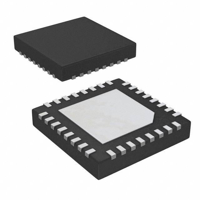
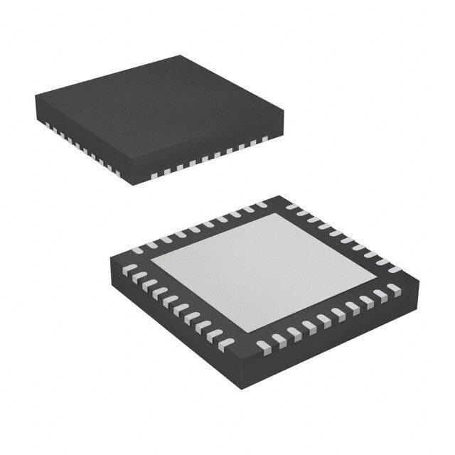
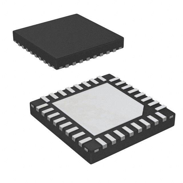
| 供应商器件封装 | 32-QFN(5x5) |
| 包装 | 管件 |
| 安装类型 | 表面贴装 |
| 封装/外壳 | 32-VFQFN 裸露焊盘 |
| 工作温度 | -40°C ~ 85°C |
| 应用 | 控制器,Intel VR11,AMD CPU |
| 标准包装 | 60 |
| 电压-输入 | 5 V ~ 12 V |
| 电压-输出 | 0.38 V ~ 1.6 V |
| 输出数 | 1 |


- 商务部:美国ITC正式对集成电路等产品启动337调查
- 曝三星4nm工艺存在良率问题 高通将骁龙8 Gen1或转产台积电
- 太阳诱电将投资9.5亿元在常州建新厂生产MLCC 预计2023年完工
- 英特尔发布欧洲新工厂建设计划 深化IDM 2.0 战略
- 台积电先进制程称霸业界 有大客户加持明年业绩稳了
- 达到5530亿美元!SIA预计今年全球半导体销售额将创下新高
- 英特尔拟将自动驾驶子公司Mobileye上市 估值或超500亿美元
- 三星加码芯片和SET,合并消费电子和移动部门,撤换高东真等 CEO
- 三星电子宣布重大人事变动 还合并消费电子和移动部门
- 海关总署:前11个月进口集成电路产品价值2.52万亿元 增长14.8%


PDF Datasheet 数据手册内容提取
DATASHEET ISL6314 FN6455 Single-Phase Buck PWM Controller with Integrated MOSFET Drivers for Intel Rev 2.00 VR11 and AMD Applications Oct 8, 2009 The ISL6314 single-phase PWM control IC provides a Features precision voltage regulation system for advanced • Integrated-driver Single-Phase Power Conversion microprocessors. This controller IC maintains the same features as the multi-phase product family, but reduces the • Precision Core Voltage Regulation output to a single-phase, for lower current systems. By - Differential Remote Voltage Sensing reducing the number of external parts, this integration is - ±0.5% System Accuracy Over-Temperature optimized for a cost and space saving power management - Adjustable Reference-Voltage Offset solution. • Optimal Transient Response One outstanding feature of this controller IC is its - Adaptive Phase Alignment (APA) multi-processor compatibility, allowing it to work with both - Active Pulse Positioning (APP) Modulation Intel and AMD microprocessors. Included are programmable VID codes for Intel VR11 as well as AMD 5-bit and 6-bit DAC • Fully Differential, Continuous DCR Current Sensing tables. A circuit is provided for remote voltage sensing, - Accurate Load Line Programming compensating for any potential difference between remote • Variable Gate Drive Bias: 5V to 12V and local grounds. The output voltage can also be positively or negatively offset through the use of a single external • Multi-Processor Compatible resistor. - Intel VR11 Mode of Operation - AMD Mode of Operation Another unique feature of the ISL6314 is the addition of a circuit that allows optimizing compensation to be added for • Microprocessor Voltage Identification Inputs flatter load transient response and well controlled dynamic - 8-Bit DAC VID response. - Selectable Between Intel VR11, AMD 5-bit, and AMD 6-bit DAC Tables The ISL6314 also includes advanced control loop features - Dynamic VID Technology for optimal transient response to load apply and removal. One of these features is highly accurate, fully differential, • Overcurrent Protection continuous DCR current sensing for load line programming. • Multi-tiered Overvoltage Protection Active Pulse Positioning (APP) and Adaptive Phase Alignment (APA) are two other unique features, allowing for • Digital Soft-Start quicker initial response to high di/dt load transients; the • Selectable Operation Frequency up to 1.0MHz number of output bulk capacitors can be reduced, helping to • Pb-Free (RoHS compliant) reduce cost. Ordering Information Protection features of this controller IC include a set of sophisticated overvoltage, undervoltage, and overcurrent PART TEMP. protection. Furthermore, the ISL6314 includes protection NUMBER PART RANGE PACKAGE PKG. (Note) MARKING (°C) (Pb-free) DWG. # against an open circuit on the remote sensing inputs. Combined, these features provide advanced protection for the ISL6314CRZ* ISL6314 CRZ 0 to +70 32 Ld 5x5 QFN L32.5x5B microprocessor and power system. ISL6314IRZ* ISL6314 IRZ -40 to +85 32 Ld 5x5 QFN L32.5x5B *Add “-T” suffix for tape and reel. Please refer to TB347 for details on reel specifications. NOTE: These Intersil Pb-free plastic packaged products employ special Pb-free material sets, molding compounds/die attach materials, and 100% matte tin plate plus anneal (e3 termination finish, which is RoHS compliant and compatible with both SnPb and Pb-free soldering operations). Intersil Pb-free products are MSL classified at Pb-free peak reflow temperatures that meet or exceed the Pb-free requirements of IPC/JEDEC J STD-020. FN6455 Rev 2.00 Page 1 of 32 Oct 8, 2009
ISL6314 Pinout ISL6314 (32 LD QFN) TOP VIEW 7 0 1 2 3 4 5 6 D D D D D D D D VI VI VI VI VI VI VI VI 32 31 30 29 28 27 26 25 PGOOD 1 24 PHASE SS 2 23 UGATE FS 3 22 BOOT REF 4 21 LGATE 33 GND OFS 5 20 NC APA 6 19 PVCC COMP 7 18 VCC DVC 8 17 EN 9 10 11 12 13 14 15 16 FB VDIFF RGND VSEN OCSET ISENO ISEN- ISEN+ ISL6314 Integrated Driver Block Diagram PVCC BOOT UGATE PWM 20k GATE SHOOT- CONTROL THROUGH PHASE LOGIC PROTECTION SOFT-START AND 10k FAULT LOGIC LGATE FN6455 Rev 2.00 Page 2 of 32 Oct 8, 2009
ISL6314 Block Diagram ISENO OCSET PGOOD EN ISEN- 100µA ISEN+ ISEN AMP OC RGND VSEN x1 FSD VDIFF 0.85V OPEN SENSE LINE DETECT UNDERVOLTAGE SOFT-START DETECTION AND LOGIC FAULT LOGIC VCC POWER-ON OVERVOLTAGE RESET PVCC DETECTION LOGIC FS FS/DROOP FSD SELECT BOOT SS MSOEDLEE/DCATC MOSFET UGATE DRIVER PHASE VID7 LGATE VID6 VID5 DYNAMIC VID4 VID VID3 D/A CLOCK AND MODULATOR VID2 WAVEFORM VID1 2k GENERATOR VID0 DVC x2 100µA REF E/A PWM FB COMP ADAPTIVE PHASE ALLIGNMENT APA CIRCUITRY OFS OFFSET GND FN6455 Rev 2.00 Page 3 of 32 Oct 8, 2009
ISL6314 Typical Application - ISL6314 FB DVCVDIFFVSEN RGND COMP APA Typical Applications +5V 1. PVCC = 12V; VIN =12V; VCC 2. PVCC = 5V; VIN = 19V; other combinations are also possible OFS PVCC VIN FS REF PVCC BOOT SS UGATE PHASE ISL6314 LGATE LOAD VID7 VID6 VID5 VID4 VID3 VID2 VID1 VID0 PGOOD EN GND ISEN+OCSET ISENO ISEN- CCOMP ROCSET Rs RCOMP FN6455 Rev 2.00 Page 4 of 32 Oct 8, 2009
ISL6314 Typical Application - ISL6314 with NTC Thermal Compensation FB DVCVDIFFVSEN RGND COMP APA +5V VCC OFS FS +12V REF PVCC BOOT PLACE IN CLOSE PROXIMITY SS UGATE PHASE ISL6314 NTC LGATE LOAD VID7 VID6 VID5 VID4 VID3 VID2 VID1 VID0 PGOOD EN GND ISEN+OCSETISENO ISEN- CCOMP ROCSET Rs RCOMP FN6455 Rev 2.00 Page 5 of 32 Oct 8, 2009
ISL6314 Absolute Maximum Ratings Thermal Information Supply Voltage, VCC. . . . . . . . . . . . . . . . . . . . . . . . . . .-0.3V to +6V Thermal Resistance JA (°C/W) JC (°C/W) Supply Voltage, PVCC. . . . . . . . . . . . . . . . . . . . . . . . .-0.3V to +15V QFN Package (Notes 1, 2). . . . . . . . . . 32 3.5 Absolute Boot Voltage, VBOOT . . . . . . . .GND - 0.3V to GND + 36V Maximum Junction Temperature . . . . . . . . . . . . . . . . . . . . . .+150°C Phase Voltage, VPHASE . . . . . . . . . . . . . . . . . . . . . . . . . . . . . . . . . . Maximum Storage Temperature Range. . . . . . . . . .-65°C to +150°C GND - 8V (<400ns, 20µJ) to 30V (<200ns, VBOOT-PHASE = 5V) Pb-Free Reflow Profile. . . . . . . . . . . . . . . . . . . . . . . . .see link below Upper Gate Voltage, VUGATE . . . .VPHASE - 0.3V to VBOOT + 0.3V http://www.intersil.com/pbfree/Pb-FreeReflow.asp VPHASE - 3.5V (<100ns Pulse Width, 2µJ) to VBOOT + 0.3V Lower Gate Voltage, VLGATE. . . . . . . . GND - 0.3V to PVCC + 0.3V Recommended Operating Conditions GND - 5V (<100ns Pulse Width, 2µJ) to PVCC+ 0.3V Input, Output, or I/O Voltage . . . . . . . . . GND - 0.3V to VCC + 0.3V VCC Supply Voltage . . . . . . . . . . . . . . . . . . . . . . . . . . . . . .+5V ±5% PVCC Supply Voltage . . . . . . . . . . . . . . . . . . . . . . .+5V to 12V ±5% Ambient Temperature ISL6314CRZ . . . . . . . . . . . . . . . . . . . . . . . . . . . . . . 0°C to +70°C ISL6314IRZ . . . . . . . . . . . . . . . . . . . . . . . . . . . . . .-40°C to +85°C CAUTION: Do not operate at or near the maximum ratings listed for extended periods of time. Exposure to such conditions may adversely impact product reliability and result in failures not covered by warranty. NOTES: 1. JA is measured in free air with the component mounted on a high effective thermal conductivity test board with “direct attach” features. See Tech Brief TB379. 2. For JC, the “case temp” location is the center of the exposed metal pad on the package underside. Electrical Specifications Recommended Operating Conditions, Unless Otherwise Specified. Parameters with MIN and/or MAX limits are 100% tested at +25°C, unless otherwise specified. Temperature limits established by characterization and are not production tested. PARAMETER TEST CONDITIONS MIN TYP MAX UNITS BIAS SUPPLIES Input Bias Supply Current IVCC; VCC = 5V; EN = high, 9 11.4 16 mA notswitching; Gate Drive Bias Current - PVCC Pin IPVCC; PVCC = 12V; EN = high, 1 2 4 mA high, not switching VCC POR (Power-On Reset) Threshold VCC rising 4.25 4.38 4.50 V VCC falling 3.75 3.88 4.00 V PVCC POR (Power-On Reset) Threshold PVCC rising 4.25 4.38 4.50 V PVCC falling 3.75 3.88 4.00 V PWM MODULATOR Oscillator Frequency Accuracy, fSW RT = 100k (± 0.1%) 225 250 275 kHz (ISL6314CRZ) Oscillator Frequency Accuracy, fSW RT = 100k (± 0.1%) 215 250 280 kHz (ISL6314IRZ) Adjustment Range of Switching Frequency (Note 3) 0.08 - 1.0 MHz Oscillator Ramp Amplitude, VP-P (Note 3) - 1.50 - V CONTROL THRESHOLDS EN Rising Threshold 0.84 0.86 0.88 V EN Hysteresis - 110 - mV REFERENCE AND DAC System Accuracy (1.000V to 1.600V) -0.5 - 0.5 % System Accuracy (0.600V to 1.000V) -1.0 - 1.0 % System Accuracy (0.375V to 0.600V) -2.0 - 2.0 % VIDx Input Low Voltage (INTEL) Pins VID0 to VID7 - - 0.4 V FN6455 Rev 2.00 Page 6 of 32 Oct 8, 2009
ISL6314 Electrical Specifications Recommended Operating Conditions, Unless Otherwise Specified. Parameters with MIN and/or MAX limits are 100% tested at +25°C, unless otherwise specified. Temperature limits established by characterization and are not production tested. (Continued) PARAMETER TEST CONDITIONS MIN TYP MAX UNITS VIDx Input High Voltage (INTEL) Pins VID0 to VID7 0.8 - - V VIDx Input Low Voltage (AMD) Pins VID0 to VID7 - - 0.8 V VIDx Input High Voltage (AMD) Pins VID0 to VID7 1.4 - - V VIDx Pull-Up Current (INTEL) Pins VID0 to VID7; VIDx = 0V - -40 - µA VIDx Pull-Down Current (AMD) Pins VID0 to VID7; VIDx = 0.5V - 20 - µA PIN-ADJUSTABLE OFFSET OFS Sink Current Accuracy (Negative Offset) ROFS = 32.4kfrom OFS to 47.0 49.4 53.0 µA VCC OFS Source Current Accuracy ROFS = 6.04kfrom OFS to 47.0 49.7 53.0 µA (PositiveOffset) GND ERROR AMPLIFIER DC Gain RL = 10k to ground, (Note 3) - 96 - dB Gain-Bandwidth Product CL = 100pF, RL = 10k to - 40 - MHz ground, (Note 3) Slew Rate CL = 100pF, load = ±400µA, - 20 - V/µs (Note 3) Maximum Output Voltage Load = 1mA 3.90 4.20 - V Minimum Output Voltage Load = -1mA - 1.20 1.4 V SOFT-START RAMP Soft-Start Ramp Rate VR11, RSS = 100k - 1.25 - mV/µs AMD, RSS = 100k - 1.25 - mV/µs Adjustment Range of Soft-Start Ramp Rate 0.156 - 6.25 mV/µs (Note 3) OVERCURRENT PROTECTION OCSET Trip Current (ISL6314CRZ) 94 100 106 µA OCSET Trip Current (ISL6314IRZ) 93 100 107 µA OCSET Accuracy OCSET and ISUM Difference -5 0 5 mV ISENO Offset -1.7 0 1.7 mV PROTECTION Undervoltage Threshold VSEN falling VDAC - 325 VDAC - 350mV VDAC - 375 V Undervoltage Hysteresis VSEN rising - 100 - mV Overvoltage Threshold During Soft-Start VR11 and AMD 1.24 1.27 1.30 V Overvoltage Threshold (Default) VR11, VSEN rising VDAC + 150mV VDAC + 175mV VDAC + 200mV V AMD, VSEN rising VDAC + 200mV VDAC + 225mV VDAC + 250mV V Overvoltage Hysteresis VSEN falling - 100 - mV PGOOD Output Sink Current PGOOD = 0.4V - 7.5 - mA OVER-TEMPERATURE SHUTDOWN (Note 3) Thermal Shutdown Setpoint - 160 - °C Thermal Recovery Setpoint - 100 - °C FN6455 Rev 2.00 Page 7 of 32 Oct 8, 2009
ISL6314 Electrical Specifications Recommended Operating Conditions, Unless Otherwise Specified. Parameters with MIN and/or MAX limits are 100% tested at +25°C, unless otherwise specified. Temperature limits established by characterization and are not production tested. (Continued) PARAMETER TEST CONDITIONS MIN TYP MAX UNITS SWITCHING TIME (Note 3) UGATE Rise Time tRUGATE; VPVCC = 12V, 3nF - 26 - ns load, 10% to 90% LGATE Rise Time tRLGATE; VPVCC = 12V, 3nF - 18 - ns load, 10% to 90% UGATE Fall Time tFUGATE; VPVCC = 12V, 3nF - 18 - ns load, 90% to 10% LGATE Fall Time tFLGATE; VPVCC = 12V, 3nF - 12 - ns load, 90% to 10% UGATE Turn-On Non-Overlap tPDHUGATE; VPVCC = 12V, 3nF - 10 - ns load, adaptive LGATE Turn-On Non-Overlap tPDHLGATE; VPVCC = 12V, 3nF - 10 - ns load, adaptive GATE DRIVE RESISTANCE (Note 3) Upper Drive Source Resistance VPVCC = 12V, 15mA source 1.25 2.0 3.0 current Upper Drive Sink Resistance VPVCC = 12V, 15mA sink 0.9 1.65 3.0 current Lower Drive Source Resistance VPVCC = 12V, 15mA source 0.85 1.25 2.2 current Lower Drive Sink Resistance VPVCC = 12V, 15mA sink 0.60 0.80 1.35 current NOTE: 3. Limits should be considered typical and are not production tested. Timing Diagram tPDHUGATE tRUGATE tFUGATE UGATE LGATE tFLGATE tRLGATE tPDHLGATE FN6455 Rev 2.00 Page 8 of 32 Oct 8, 2009
ISL6314 Functional Pin Description FB and COMP (Pins 9, 7) These pins are the internal error amplifier inverting input and VCC (Pin 18) output respectively. The FB pin, COMP pin, and the VDIFF VCC is the bias supply for the ICs small-signal circuitry. pins are tied together through external R-C networks to Connect this pin to a +5V supply and decouple using a compensate the regulator. quality 0.1µF ceramic capacitor. DVC (Pin 8) PVCC (Pin 19) A series resistor and capacitor can be connected from the This pin is the power supply pin for the channel MOSFET DVC pin to the FB pin to compensate and smooth dynamic drivers, and can be connected to any voltage from +5V to VID transitions. +12V depending on the desired MOSFET gate-drive level. OCSET (Pin 13) Decouple this pin with a quality 1.0µF ceramic capacitor. This is the overcurrent set pin. Placing a resistor from GND (Pin 33 = Metal Pad) OCSET pin to ISENO allows a 100µA current to flow out of GND is the bias and reference ground for the IC, connected this pin, producing a voltage reference. Internal circuitry to the metal pad under the IC. compares the voltage at OCSET to the voltage at ISEN-, and EN (Pin 17) if ISEN- ever exceeds OCSET, the overcurrent protection activates. This pin is a threshold-sensitive (approximately 0.85V) enable input for the controller. Held low, this pin disables controller APA (Pin 6) operation. Pulled high, the pin enables the controller for This is the Adaptive Phase Alignment set pin. A 100µA operation. current flows out the APA pin and by tying a resistor from this FS (Pin 3) pin to COMP the trip level for the Adaptive Phase Alignment circuitry can be set. A resistor, RT, tied to this pin sets the channel switching frequency of the controller. Refer to Equation 42 for proper REF (Pin 4) resistor calculation. The REF input pin is the positive input of the error amplifier. It The FS pin also controls whether the droop voltage (as is internally connected to the DAC output through a 2k described under pins ISENO, ISEN-, ISEN+) is added to the resistor. A capacitor is used between the REF pin and ground differential remote-sense amplifier’s output (VDIFF). Tying the to smooth the voltage transition during soft-start and Dynamic RT resistor to ground connects droop voltage, allowing the VID transitions. This pin can also be returned to RGND if desired. converter to incorporate output voltage droop proportional to the output current. Tying the RT resistor to VCC disconnects NC (Pin 20) the droop voltage. This pin is presently NC (No Connect), but is reserved for a VID0, VID1, VID2, VID3, VID4, VID5, VID6, and VID7 future function. (Pins 31, 30, 29, 28, 27, 26, 25, 32) OFS (Pin 5) These are the inputs for the internal DAC that provide the The OFS pin provides a means to program a DC current for reference voltage for output regulation. These pins respond to generating an offset voltage across the resistor between FB TTL logic thresholds. These pins are internally pulled high, to and VDIFF. The offset current is generated via an external approximately 1.2V, by 40µA internal current sources for Intel resistor and precision internal voltage references. The polarity modes of operation, and pulled low by 20µA internal current is selected by connecting the resistor to GND (for positive sources for AMD modes of operation. The internal pull-up offset) or to VCC (for negative offset). For no offset, the OFS current decreases to 0 as the VID voltage approaches the pin should be left unconnected. internal pull-up voltage. All VID pins are compatible with external pull-up voltages not exceeding the IC’s bias voltage UGATE (Pin 23) (VCC). Connect this pin to the corresponding upper MOSFET gate. VSEN (Pin 12) This pin is used to control the upper MOSFET and is monitored for shoot-through prevention purposes. This pin senses the microprocessor’s CORE voltage. Connect this pin to the CORE voltage sense pin or point of the BOOT (Pin 22) microprocessor. This pin provides the bias voltage for the upper MOSFET drive. Connect this pin to appropriately-chosen external RGND (Pin 11) bootstrap capacitors. Internal bootstrap diodes connected to This pin senses the local ground voltage of the the PVCC pin provides the necessary bootstrap charge. microprocessor. Connect this pin to the Ground sense pin or point of the microprocessor. FN6455 Rev 2.00 Page 9 of 32 Oct 8, 2009
ISL6314 PHASE (Pin 24) Operation Connect this pin to the source of the upper MOSFET. This Power Conversion pin is the return path for the upper MOSFET drive. The ISL6314 controller helps simplify implementation by LGATE (Pin 21) integrating vital functions and requiring minimal external This pin is used to control the lower MOSFET. Connect this components. The “Block Diagram” on page3 provides a top pin to the lower MOSFET gate. level view of the single-phase power conversion using the ISL6314 controller. SS (Pin 2) A resistor, RSS, placed from SS to VCC or GND will set the soft-start ramp slope. Refer to Equations 16 and 17 for proper resistor calculation. IL, 7A/DIV The state of the SS pin also selects which of the available DAC tables will be used to decode the VID inputs and puts the controller into the corresponding mode of operation. For Intel VR11 mode of operation the RSS resistor should be tied to GND. AMD compliance is selected if the RSS resistor is tied to VCC (once in AMD mode, the VID7 bit selects 5-bit DAC if set to a logic high, or 6-bit DAC if set to a logic low). PGOOD (Pin 1) PWM, 5V/DIV For Intel mode of operation, PGOOD indicates whether VSEN 1µs/DIV is within specified overvoltage and undervoltage limits after a FIGURE 1. PWM AND INDUCTOR-CURRENT WAVEFORMS fixed delay from the end of soft-start. If VSEN exceeds these FOR 1-PHASE CONVERTER limits, or if an overcurrent event occurs, or if the part is Output Ripple disabled, PGOOD is pulled low. PGOOD is always low prior to Figure 1 illustrates the output ripple. The PWM current forms the end of soft-start. the AC ripple current and the DC load current. The For AMD modes of operation, PGOOD will always be high as peak-to-peak current about 7A, and the DC components of long as VSEN is within the specified undervoltage/overvoltage the inductor current feeds the load. window and soft-start has ended. PGOOD only goes low if To understand the ripple current amplitude, examine VSEN is outside this window. Equation 1 representing a single channel peak-to-peak ISENO, ISEN-, and ISEN+ (Pins 14, 15, 16) inductor current. ISEN-, ISEN+, and ISENO are the DCR current sense V –V V amplifier’s negative input, positive input, and output IP-P= -------I--N------L--------O-f----U----T--V-------------O----U-----T-- (EQ. 1) S IN respectively. For accurate DCR current sensing, connect a resistor from the phase node to ISEN- and connect ISEN+ to In Equation 1, VIN and VOUT are the input and output voltages respectively, L is the single-channel inductor value, the output inductor, roughly VOUT. A parallel R-C feedback circuit connected between ISEN- and ISENO will then create and fS is the switching frequency. a voltage from ISEN+ to ISENO proportional to the voltage The output capacitors conduct the ripple component of the drop across the inductor DCR. This voltage is referred to as inductor current. Output voltage ripple is a function of the droop voltage and is added to the differential capacitance, capacitor equivalent series resistance (ESR), remote-sense amplifier’s output. and inductor ripple current. Reducing the inductor ripple current allows the designer to use fewer or less costly output An optional 0.001µF to 0.01µF ceramic capacitor can be capacitors. Equation 2 shows the approximation for the placed from the ISEN+ pin to the ISEN- pin to help reduce output voltage ripple. common mode noise that might be introduced by the layout. VDIFF (Pin 10) VP-P = IP-P ESR (EQ. 2) VDIFF is the output of the differential remote-sense amplifier. Adaptive Phase Alignment (APA) The voltage on this pin is equal to the difference between To improve the transient response, the ISL6314 implements VSEN and RGND (VOUT) added to the difference between Intersil’s proprietary Adaptive Phase Alignment (APA) ISEN+ and ISENO (droop). VDIFF therefore represents the technique, which turns on the channel during large current VOUT voltage plus the droop voltage. The state of the FS pin step transient events. determines whether the droop voltage is added or not. FN6455 Rev 2.00 Page 10 of 32 Oct 8, 2009
ISL6314 The PWM output state is driven by the position of the error EXTERNAL CIRCUIT ISL6314 INTERNAL CIRCUIT amplifier output signal, VCOMP, as illustrated in Figure 3. At the beginning of each PWM time interval, this VCOMP signal APA is compared to the internal modulator waveform. As long as the VCOMP voltage is lower then the modulator waveform - 100µA + voltage, the PWM signal is commanded low. The internal CAPA RAPA VAPA,TRIP APA MOSFET driver detects the low state of the PWM signal and + - turns off the upper MOSFET and turns on the lower TO APA LOW CIRCUITRY synchronous MOSFET. When the VCOMP voltage crosses PASS COMP FILTER the modulator ramp, the PWM output transitions high, turning off the synchronous MOSFET and turning on the ERROR upper MOSFET. The PWM signal will remain high until the AMPLIFIER - + VCOMP voltage crosses the modulator ramp again. When this occurs, the PWM signal will transition low again. During each PWM time interval, the PWM signal can only FIGURE 2. ADAPTIVE PHASE ALIGNMENT DETECTION transition high once. Once PWM transitions high, it can not As Figure 2 shows, the APA circuitry works by monitoring the transition high again until the beginning of the next PWM voltage on the APA pin and comparing it to a filtered copy of time interval. This prevents the occurrence of double PWM the voltage on the COMP pin. The voltage on the APA pin is pulses occurring during a single period. a copy of the COMP pin voltage that has been negatively offset. If the APA pin exceeds the filtered COMP pin voltage VCOMP + PWM TO GATE an APA event occurs and the channel is forced on. MODULATOR CONTROL RAMP - LOGIC The APA trip level is the amount of DC offset between the WAVEFORM COMP pin and the APA pin. This is the voltage excursion FIGURE 3. CHANNEL PWM FUNCTION that the APA and COMP pin must have during a transient event to activate the Adaptive Phase Alignment circuitry. Output Voltage Setting This APA trip level is set through a resistor, RAPA, that connects from the APA pin to the COMP pin. A 100µA The ISL6314 uses a digital to analog converter (DAC) to current flows across RAPA into the APA pin to set the APA generate a reference voltage based on the logic signals at trip level as described in Equation 3. An APA trip level of the VID pins. The DAC decodes the logic signals into one of 500mV is recommended for most applications. A 1000pF the discrete voltages shown in Tables 2, 3 or 4. In the Intel capacitor, CAPA, should also be placed across the RAPA VR11 mode of operation, each VID pin is pulled up to an resistor to help with noise immunity. internal 1.2V voltage by a weak current source (40µA), which decreases to 0A as the voltage at the VID pin varies VAPATRIP = RAPA10010–6 (EQ. 3) from 0 to the internal 1.2V pull-up voltage. In AMD modes of operation, the VID pins are pulled low by a weak 20µA current source. External pull-up resistors or active-high Active Pulse Positioning (APP) Modulated PWM output stages can augment the pull-up current sources, up to Operation a voltage of 5V. The ISL6314 uses a proprietary Active Pulse Positioning (APP) modulation scheme to control the internal PWM .The ISL6314 accommodates three different DAC ranges: signals that command each channel’s driver to turn their Intel VR11, AMD K8/K9 5-bit, and AMD 6-bit. The state of upper and lower MOSFETs on and off. The time interval in the SS and VID7 pins decide which DAC version is active. which a PWM signal can occur is generated by an internal Refer to Table 1 for a description of how to select the desired clock, whose cycle time is the inverse of the switching DAC version. frequency set by the resistor connected to the FS pin. The advantage of Intersil’s proprietary Active Pulse Positioning (APP) modulator is that the PWM signal has the ability to turn on at any point during this PWM time interval, and turn off immediately after the PWM signal has transitioned high. This is important because is allows the controller to quickly respond to output voltage drops associated with current load spikes, while avoiding the ring back affects associated with other modulation schemes. FN6455 Rev 2.00 Page 11 of 32 Oct 8, 2009
ISL6314 TABLE 1. ISL6314 DAC SELECT AND FUNCTION TABLE TABLE 2. VR11 VOLTAGE IDENTIFICATION CODES (Continued) DAC VERSION SS PIN VID7 PIN VID7 VID6 VID5 VID4 VID3 VID2 VID1 VID0 VDAC INTEL VR11 RSS resistor tied to - 0 0 0 1 1 0 1 1 1.44375 GND 0 0 0 1 1 1 0 0 1.43750 AMD 5-BIT RSS resistor tied to high 0 0 0 1 1 1 0 1 1.43125 VCC 0 0 0 1 1 1 1 0 1.42500 AMD 6-BIT RSS resistor tied to low VCC 0 0 0 1 1 1 1 1 1.41875 0 0 1 0 0 0 0 0 1.41250 TIE RESISTOR to OPEN TIE RESISTOR to 0 0 1 0 0 0 0 1 1.40625 VCC GND 0 0 1 0 0 0 1 0 1.40000 RSS: AMD Tables - RSS: Intel Table 0 0 1 0 0 0 1 1 1.39375 ROFS: Negative No Offset ROFS: Positive 0 0 1 0 0 1 0 0 1.38750 RT: No Droop - RT: Droop 0 0 1 0 0 1 0 1 1.38125 TABLE 2. VR11 VOLTAGE IDENTIFICATION CODES 0 0 1 0 0 1 1 0 1.37500 VID7 VID6 VID5 VID4 VID3 VID2 VID1 VID0 VDAC 0 0 1 0 0 1 1 1 1.36875 0 0 0 0 0 0 0 0 OFF 0 0 1 0 1 0 0 0 1.36250 0 0 0 0 0 0 0 1 OFF 0 0 1 0 1 0 0 1 1.35625 0 0 0 0 0 0 1 0 1.60000 0 0 1 0 1 0 1 0 1.35000 0 0 0 0 0 0 1 1 1.59375 0 0 1 0 1 0 1 1 1.34375 0 0 0 0 0 1 0 0 1.58750 0 0 1 0 1 1 0 0 1.33750 0 0 0 0 0 1 0 1 1.58125 0 0 1 0 1 1 0 1 1.33125 0 0 0 0 0 1 1 0 1.57500 0 0 1 0 1 1 1 0 1.32500 0 0 0 0 0 1 1 1 1.56875 0 0 1 0 1 1 1 1 1.31875 0 0 0 0 1 0 0 0 1.56250 0 0 1 1 0 0 0 0 1.31250 0 0 0 0 1 0 0 1 1.55625 0 0 1 1 0 0 0 1 1.30625 0 0 0 0 1 0 1 0 1.55000 0 0 1 1 0 0 1 0 1.30000 0 0 0 0 1 0 1 1 1.54375 0 0 1 1 0 0 1 1 1.29375 0 0 0 0 1 1 0 0 1.53750 0 0 1 1 0 1 0 0 1.28750 0 0 0 0 1 1 0 1 1.53125 0 0 1 1 0 1 0 1 1.28125 0 0 0 0 1 1 1 0 1.52500 0 0 1 1 0 1 1 0 1.27500 0 0 0 0 1 1 1 1 1.51875 0 0 1 1 0 1 1 1 1.26875 0 0 0 1 0 0 0 0 1.51250 0 0 1 1 1 0 0 0 1.26250 0 0 0 1 0 0 0 1 1.50625 0 0 1 1 1 0 0 1 1.25625 0 0 0 1 0 0 1 0 1.50000 0 0 1 1 1 0 1 0 1.25000 0 0 0 1 0 0 1 1 1.49375 0 0 1 1 1 0 1 1 1.24375 0 0 0 1 0 1 0 0 1.48750 0 0 1 1 1 1 0 0 1.23750 0 0 0 1 0 1 0 1 1.48125 0 0 1 1 1 1 0 1 1.23125 0 0 0 1 0 1 1 0 1.47500 0 0 1 1 1 1 1 0 1.22500 0 0 0 1 0 1 1 1 1.46875 0 0 1 1 1 1 1 1 1.21875 0 0 0 1 1 0 0 0 1.46250 0 1 0 0 0 0 0 0 1.21250 0 0 0 1 1 0 0 1 1.45625 0 1 0 0 0 0 0 1 1.20625 0 0 0 1 1 0 1 0 1.45000 0 1 0 0 0 0 1 0 1.20000 FN6455 Rev 2.00 Page 12 of 32 Oct 8, 2009
ISL6314 TABLE 2. VR11 VOLTAGE IDENTIFICATION CODES (Continued) TABLE 2. VR11 VOLTAGE IDENTIFICATION CODES (Continued) VID7 VID6 VID5 VID4 VID3 VID2 VID1 VID0 VDAC VID7 VID6 VID5 VID4 VID3 VID2 VID1 VID0 VDAC 0 1 0 0 0 0 1 1 1.19375 0 1 1 0 1 0 1 1 0.94375 0 1 0 0 0 1 0 0 1.18750 0 1 1 0 1 1 0 0 0.93750 0 1 0 0 0 1 0 1 1.18125 0 1 1 0 1 1 0 1 0.93125 0 1 0 0 0 1 1 0 1.17500 0 1 1 0 1 1 1 0 0.92500 0 1 0 0 0 1 1 1 1.16875 0 1 1 0 1 1 1 1 0.91875 0 1 0 0 1 0 0 0 1.16250 0 1 1 1 0 0 0 0 0.91250 0 1 0 0 1 0 0 1 1.15625 0 1 1 1 0 0 0 1 0.90625 0 1 0 0 1 0 1 0 1.15000 0 1 1 1 0 0 1 0 0.90000 0 1 0 0 1 0 1 1 1.14375 0 1 1 1 0 0 1 1 0.89375 0 1 0 0 1 1 0 0 1.13750 0 1 1 1 0 1 0 0 0.88750 0 1 0 0 1 1 0 1 1.13125 0 1 1 1 0 1 0 1 0.88125 0 1 0 0 1 1 1 0 1.12500 0 1 1 1 0 1 1 0 0.87500 0 1 0 0 1 1 1 1 1.11875 0 1 1 1 0 1 1 1 0.86875 0 1 0 1 0 0 0 0 1.11250 0 1 1 1 1 0 0 0 0.86250 0 1 0 1 0 0 0 1 1.10625 0 1 1 1 1 0 0 1 0.85625 0 1 0 1 0 0 1 0 1.10000 0 1 1 1 1 0 1 0 0.85000 0 1 0 1 0 0 1 1 1.09375 0 1 1 1 1 0 1 1 0.84375 0 1 0 1 0 1 0 0 1.08750 0 1 1 1 1 1 0 0 0.83750 0 1 0 1 0 1 0 1 1.08125 0 1 1 1 1 1 0 1 0.83125 0 1 0 1 0 1 1 0 1.07500 0 1 1 1 1 1 1 0 0.82500 0 1 0 1 0 1 1 1 1.06875 0 1 1 1 1 1 1 1 0.81875 0 1 0 1 1 0 0 0 1.06250 1 0 0 0 0 0 0 0 0.81250 0 1 0 1 1 0 0 1 1.05625 1 0 0 0 0 0 0 1 0.80625 0 1 0 1 1 0 1 0 1.05000 1 0 0 0 0 0 1 0 0.80000 0 1 0 1 1 0 1 1 1.04375 1 0 0 0 0 0 1 1 0.79375 0 1 0 1 1 1 0 0 1.03750 1 0 0 0 0 1 0 0 0.78750 0 1 0 1 1 1 0 1 1.03125 1 0 0 0 0 1 0 1 0.78125 0 1 0 1 1 1 1 0 1.02500 1 0 0 0 0 1 1 0 0.77500 0 1 0 1 1 1 1 1 1.01875 1 0 0 0 0 1 1 1 0.76875 0 1 1 0 0 0 0 0 1.01250 1 0 0 0 1 0 0 0 0.76250 0 1 1 0 0 0 0 1 1.00625 1 0 0 0 1 0 0 1 0.75625 0 1 1 0 0 0 1 0 1.00000 1 0 0 0 1 0 1 0 0.75000 0 1 1 0 0 0 1 1 0.99375 1 0 0 0 1 0 1 1 0.74375 0 1 1 0 0 1 0 0 0.98750 1 0 0 0 1 1 0 0 0.73750 0 1 1 0 0 1 0 1 0.98125 1 0 0 0 1 1 0 1 0.73125 0 1 1 0 0 1 1 0 0.97500 1 0 0 0 1 1 1 0 0.72500 0 1 1 0 0 1 1 1 0.96875 1 0 0 0 1 1 1 1 0.71875 0 1 1 0 1 0 0 0 0.96250 1 0 0 1 0 0 0 0 0.71250 0 1 1 0 1 0 0 1 0.95625 1 0 0 1 0 0 0 1 0.70625 0 1 1 0 1 0 1 0 0.95000 1 0 0 1 0 0 1 0 0.70000 FN6455 Rev 2.00 Page 13 of 32 Oct 8, 2009
ISL6314 TABLE 2. VR11 VOLTAGE IDENTIFICATION CODES (Continued) TABLE 3. AMD 5-BIT VOLTAGE IDENTIFICATION CODES (Continued) VID7 VID6 VID5 VID4 VID3 VID2 VID1 VID0 VDAC VID4 VID3 VID2 VID1 VID0 VDAC 1 0 0 1 0 0 1 1 0.69375 1 1 1 0 0 0.850 1 0 0 1 0 1 0 0 0.68750 1 1 0 1 1 0.875 1 0 0 1 0 1 0 1 0.68125 1 1 0 1 0 0.900 1 0 0 1 0 1 1 0 0.67500 1 1 0 0 1 0.925 1 0 0 1 0 1 1 1 0.66875 1 1 0 0 0 0.950 1 0 0 1 1 0 0 0 0.66250 1 0 1 1 1 0.975 1 0 0 1 1 0 0 1 0.65625 1 0 1 1 0 1.000 1 0 0 1 1 0 1 0 0.65000 1 0 1 0 1 1.025 1 0 0 1 1 0 1 1 0.64375 1 0 1 0 0 1.050 1 0 0 1 1 1 0 0 0.63750 1 0 0 1 1 1.075 1 0 0 1 1 1 0 1 0.63125 1 0 0 1 0 1.100 1 0 0 1 1 1 1 0 0.62500 1 0 0 0 1 1.125 1 0 0 1 1 1 1 1 0.61875 1 0 0 0 0 1.150 1 0 1 0 0 0 0 0 0.61250 0 1 1 1 1 1.175 1 0 1 0 0 0 0 1 0.60625 0 1 1 1 0 1.200 1 0 1 0 0 0 1 0 0.60000 0 1 1 0 1 1.225 1 0 1 0 0 0 1 1 0.59375 0 1 1 0 0 1.250 1 0 1 0 0 1 0 0 0.58750 0 1 0 1 1 1.275 1 0 1 0 0 1 0 1 0.58125 0 1 0 1 0 1.300 1 0 1 0 0 1 1 0 0.57500 0 1 0 0 1 1.325 1 0 1 0 0 1 1 1 0.56875 0 1 0 0 0 1.350 1 0 1 0 1 0 0 0 0.56250 0 0 1 1 1 1.375 1 0 1 0 1 0 0 1 0.55625 0 0 1 1 0 1.400 1 0 1 0 1 0 1 0 0.55000 0 0 1 0 1 1.425 1 0 1 0 1 0 1 1 0.54375 0 0 1 0 0 1.450 1 0 1 0 1 1 0 0 0.53750 0 0 0 1 1 1.475 1 0 1 0 1 1 0 1 0.53125 0 0 0 1 0 1.500 1 0 1 0 1 1 1 0 0.52500 0 0 0 0 1 1.525 1 0 1 0 1 1 1 1 0.51875 0 0 0 0 0 1.550 1 0 1 1 0 0 0 0 0.51250 1 0 1 1 0 0 0 1 0.50625 TABLE 4. AMD 6-BIT VOLTAGE IDENTIFICATION CODES 1 0 1 1 0 0 1 0 0.50000 VID5 VID4 VID3 VID2 VID1 VID0 VDAC 1 1 1 1 1 1 1 0 OFF 0 0 0 0 0 0 1.5500 1 1 1 1 1 1 1 1 OFF 0 0 0 0 0 1 1.5250 TABLE 3. AMD 5-BIT VOLTAGE IDENTIFICATION 0 0 0 0 1 0 1.5000 CODES 0 0 0 0 1 1 1.4750 VID4 VID3 VID2 VID1 VID0 VDAC 0 0 0 1 0 0 1.4500 1 1 1 1 1 Off 0 0 0 1 0 1 1.4250 1 1 1 1 0 0.800 0 0 0 1 1 0 1.4000 1 1 1 0 1 0.825 FN6455 Rev 2.00 Page 14 of 32 Oct 8, 2009
ISL6314 TABLE 4. AMD 6-BIT VOLTAGE IDENTIFICATION TABLE 4. AMD 6-BIT VOLTAGE IDENTIFICATION CODES (Continued) CODES (Continued) VID5 VID4 VID3 VID2 VID1 VID0 VDAC VID5 VID4 VID3 VID2 VID1 VID0 VDAC 0 0 0 1 1 1 1.3750 1 0 1 1 1 0 0.5875 0 0 1 0 0 0 1.3500 1 0 1 1 1 1 0.5750 0 0 1 0 0 1 1.3250 1 1 0 0 0 0 0.5625 0 0 1 0 1 0 1.3000 1 1 0 0 0 1 0.5500 0 0 1 0 1 1 1.2750 1 1 0 0 1 0 0.5375 0 0 1 1 0 0 1.2500 1 1 0 0 1 1 0.5250 0 0 1 1 0 1 1.2250 1 1 0 1 0 0 0.5125 0 0 1 1 1 0 1.2000 1 1 0 1 0 1 0.5000 0 0 1 1 1 1 1.1750 1 1 0 1 1 0 0.4875 0 1 0 0 0 0 1.1500 1 1 0 1 1 1 0.4750 0 1 0 0 0 1 1.1250 1 1 1 0 0 0 0.4625 0 1 0 0 1 0 1.1000 1 1 1 0 0 1 0.4500 0 1 0 0 1 1 1.0750 1 1 1 0 1 0 0.4375 0 1 0 1 0 0 1.0500 1 1 1 0 1 1 0.4250 0 1 0 1 0 1 1.0250 1 1 1 1 0 0 0.4125 0 1 0 1 1 0 1.0000 1 1 1 1 0 1 0.4000 0 1 0 1 1 1 0.9750 1 1 1 1 1 0 0.3875 0 1 1 0 0 0 0.9500 1 1 1 1 1 1 0.3750 0 1 1 0 0 1 0.9250 Voltage Regulation 0 1 1 0 1 0 0.9000 In order to regulate the output voltage to a specified level, 0 1 1 0 1 1 0.8750 the ISL6314 uses the integrating compensation network 0 1 1 1 0 0 0.8500 shown in Figure 4. This compensation network insures that the steady-state error in the output voltage is limited only to 0 1 1 1 0 1 0.8250 the error in the reference voltage (output of the DAC) and 0 1 1 1 1 0 0.8000 offset errors in the OFS current source, remote-sense and 0 1 1 1 1 1 0.7750 error amplifiers. Intersil specifies the guaranteed tolerance of the ISL6314 to include the combined tolerances of each of 1 0 0 0 0 0 0.7625 these elements. 1 0 0 0 0 1 0.7500 The ISL6314 incorporates an internal differential 1 0 0 0 1 0 0.7375 remote-sense amplifier in the feedback path. The amplifier 1 0 0 0 1 1 0.7250 removes the voltage error encountered when measuring the output voltage relative to the controller ground reference 1 0 0 1 0 0 0.7125 point, resulting in a more accurate means of sensing output 1 0 0 1 0 1 0.7000 voltage. Connect the microprocessor sense pins to the 1 0 0 1 1 0 0.6875 non-inverting input, VSEN, and inverting input, RGND, of the 1 0 0 1 1 1 0.6750 remote-sense amplifier. The droop voltage, VDROOP, also feeds into the remote-sense amplifier. The remote-sense 1 0 1 0 0 0 0.6625 output, VDIFF, is therefore equal to the sum of the output 1 0 1 0 0 1 0.6500 voltage, VOUT, and the droop voltage. VDIFF is connected to the inverting input of the error amplifier through an external 1 0 1 0 1 0 0.6375 resistor. 1 0 1 0 1 1 0.6250 V = V –V –V (EQ. 4) 1 0 1 1 0 0 0.6125 OUT REF OFS DROOP 1 0 1 1 0 1 0.6000 FN6455 Rev 2.00 Page 15 of 32 Oct 8, 2009
ISL6314 The output of the error amplifier, VCOMP, is compared to the . sawtooth waveform to generate the PWM signal. The PWM +LVL(s) - IOUT signal controls the timing of the Internal MOSFET drivers DCR PHASE and regulates the converter output so that the voltage at FB INDUCTOR VOUT is equal to the voltage at REF. This will regulate the output IL voltage to be equal to Equation 4. The internal and external RS COUT circuitry that controls voltage regulation is illustrated in Figure 4. ISEN- EXTERNAL CIRCUIT ISL6314 INTERNAL CIRCUIT + - RC CC COMP CCOMP RCOMP ISENO VID DAC - 2k VDROOP (OPTIONAL) REF + ISEN+ CREF + ISL6314 FB - VCOMP FIGURE 5. DCR SENSING CONFIGURATION + ERROR AMPLIFIER RFB -VOFS IOFS As shown in Figure 5, a voltage, VDROOP, proportional to the VDIFF current in the channel, IOUT, feeds into the differential remote-sense amplifier. The resulting voltage at the output of the remote-sense amplifier is the sum of the output voltage VSEN + + and the droop voltage. Equation 5 shows that feeding this VOUT + voltage into the compensation network causes the regulator - RGND to adjust the output voltage so that it’s equal to the reference voltage minus the droop voltage. ISEN+ - + - The droop voltage, VDROOP, is created by sensing the VDROOP current through the output inductors. This is accomplished - ISENO DIFFERENTIAL by using a continuous DCR current sensing method. REMOTE-SENSE AMPLIFIER Inductor windings have a characteristic distributed FIGURE 4. OUTPUT VOLTAGE AND LOAD-LINE resistance or DCR (Direct Current Resistance). For REGULATION WITH OFFSET ADJUSTMENT simplicity, the inductor DCR is considered as a separate lumped quantity, as shown in Figure 5. The channel current, Load-Line (Droop) Regulation IL, flowing through the inductor, passes through the DCR. Some microprocessor manufacturers require a Equation 5 shows the S-domain equivalent voltage, VL, precisely-controlled output resistance. This dependence of across the inductor. output voltage on load current is often termed “droop” or “load line” regulation. By adding a well controlled output VLs = ILsL+DCR (EQ. 5) impedance, the output voltage can effectively be level shifted in a direction which works to achieve the load-line regulation The inductor DCR is important because the voltage dropped required by these manufacturers. across it is proportional to the channel current. By using a simple R-C network and a current sense amplifier, as shown In other cases, the designer may determine that a more in Figure 5, the voltage drop across the inductor’s DCR can cost-effective solution can be achieved by adding droop. be extracted. The output of the current sense amplifier, Droop can help to reduce the output-voltage spike that results from fast load-current demand changes. VDROOP, can be shown to be proportional to the channel current IL, shown in Equation 6. The magnitude of the spike is dictated by the ESR and ESL of the output capacitors selected. By positioning the no-load V s= --------------------------D---s-------C--------L--R---------+----1----------------------------R-----C-----O-----M-----P---I DCR (EQ. 6) voltage level near the upper specification limit, a larger DROOP sRCOMPCCOMP+1 RS L negative spike can be sustained without crossing the lower If the R-C network components are selected such that the limit. By adding a well controlled output impedance, the R-C time constant matches the inductor L/DCR time output voltage under load can effectively be level shifted down so that a larger positive spike can be sustained without constant, then VDROOP is equal to the voltage drop across the DCR, multiplied by a gain. As Equation 7 shows, crossing the upper specification limit. VDROOP is therefore proportional to the total output current, IOUT. FN6455 Rev 2.00 Page 16 of 32 Oct 8, 2009
ISL6314 . R VDIFF COMP VDROOP = -------R--------------IOUTDCR (EQ. 7) S + By simply adjusting the value of RS, the load line can be set VOFS RFB to any level, giving the converter the right amount of droop at - VREF E/A all load currents. It may also be necessary to compensate for FB any changes in DCR due to temperature. These changes cause the load line to be skewed, and cause the R-C time IOFS constant to not match the L/DCR time constant. If this becomes a problem a simple negative temperature coefficient resistor network can be used in the place of RCOMP to compensate for the rise in DCR due to temperature. Note: An optional 10nF ceramic capacitor from the ISEN+ - 1.6V pin to the ISEN- pin is recommended to help reduce any + + noise affects on the current sense amplifier due to layout 0.3V OFS - Output-Voltage Offset Programming ROFS ISL6314 The ISL6314 allows the designer to accurately adjust the GND VCC GND offset voltage by connecting a resistor, ROFS, from the OFS pin to VCC or GND. When ROFS is connected between OFS FIGURE 6. POSITIVE OFFSET OUTPUT VOLTAGE PROGRAMMING and VCC, the voltage across it is regulated to 1.6V. This causes a proportional current (IOFS) to flow into the OFS pin and out of the FB pin, providing a negative offset. If ROFS is VDIFF connected to ground, the voltage across it is regulated to 0.3V, and IOFS flows into the FB pin and out of the OFS pin, - providing a positive offset. The offset current flowing through VOFS RFB the resistor between VDIFF and FB will generate the desired + VREF E/A offset voltage which is equal to the product (IOFS x RFB). FB These functions are shown in Figures 6 and 7. IOFS Once the desired output offset voltage has been determined, use the following formulas in Equations 8 and 9 to set ROFS: For Negative Offset (connect ROFS to VCC): 1.6RFB VCC ROFS = V-------------------------- (EQ. 8) OFFSET - For Positive Offset (connect ROFS to GND): ROFS 1.6V + + R = --0---.--3--------R----F----B--- (EQ. 9) OFS - 0.3V OFS V ISL6314 OFFSET GND VCC FIGURE 7. NEGATIVE OFFSET OUTPUT VOLTAGE PROGRAMMING FN6455 Rev 2.00 Page 17 of 32 Oct 8, 2009
ISL6314 Dynamic VID Compensating Dynamic VID Transitions Modern microprocessors need to make changes to their core During a VID transition, the resulting change in voltage on voltage as part of normal operation. They direct the ISL6314 the FB pin and the COMP pin causes an AC current to flow to do this by making changes to the VID inputs. The ISL6314 through the error amplifier compensation components from is required to monitor the DAC inputs and respond to the FB to the COMP pin. This current then flows through the on-the-fly VID changes in a controlled manner, supervising a feedback resistor, RFB, and can cause the output voltage to safe output voltage transition without discontinuity or overshoot or undershoot at the end of the VID transition. In disruption. The DAC mode, ISL6314 is operating in, order to ensure the smooth transition of the output voltage determines how the controller responds to a dynamic VID during a VID change, a VID-on-the-fly compensation change. network is required. This network is composed of a resistor and capacitor in series, RDVC and CDVC, between the DVC INTEL DYNAMIC VID TRANSITIONS and the FB pin, as shown in Figure 8. When in Intel VR11 mode the ISL6314 checks the VID inputs on the positive edge of an internal 5.5MHz clock. If a new RFB IDVC = IC VDIFF code is established and it remains stable for three consecutive IC readings (0.36µs to 0.54µs), the ISL6314 recognizes the new IDVC code and changes the internal DAC reference directly to the CC RC new level. The Intel processor controls the VID transitions and CDVC RDVC is responsible for incrementing or decrementing one VID step DVC FB COMP at a time. In VR11 mode, the ISL6314 will immediately change the internal DAC reference to the new requested value as x2 - soon as the request is validated, which means the fastest REF recommended rate at which a bit change can occur is once + ERROR every 1µs. If the VID code is changed by more then one step CREF AMPLIFIER at a time, the DAC will try to track it at a 5.5MHz step rate. VDAC+RGND ISL6314 INTERNAL CIRCUIT This will likely cause an overcurrent or overvoltage fault. FIGURE 8. VID-ON-THE-FLY COMPENSATION NETWORK AMD DYNAMIC VID TRANSITIONS When running in AMD 5-bit or 6-bit modes of operation, the This VID-on-the-fly compensation network works by ISL6314 responds differently to a dynamic VID change. In the sourcing AC current into the FB node to offset the effects of AMD modes the ISL6314 still checks the VID inputs on the the AC current flowing from the FB to the COMP pin during a positive edge of an internal 5.5MHz clock. In these modes the VID transition. To create this compensation current the VID code can be changed by more than a 1-bit step at a time. If ISL6314 sets the voltage on the DVC pin to be 2x the voltage a new code is established and it remains stable for three on the REF pin. Since the error amplifier forces the voltage consecutive readings (0.36µs to 0.54µs), the ISL6314 on the FB pin and the REF pin to be equal, the resulting recognizes the change and begins slewing the DAC in voltage across the series RC between DVC and FB is equal 6.25mV steps at a stepping frequency of 345kHz until the VID to the REF pin voltage. The RC compensation components, and DAC are equal. Thus, the total time required for a VID RDVC and CDVC, can then be selected to create the desired change, tDVID, is dependent only on the size of the VID change amount of compensation current. (VVID). The amount of compensation current required is dependant The time required for a ISL6314-based converter in AMD 5-bit on the modulator gain of the system, K1, and the error DAC configuration to make a 1.1V to 1.5V reference voltage amplifier R-C components, RC and CC, that are in series change is about 186µs, as calculated using Equation 10. between the FB and COMP pins. Use Equations 11, 12, and t = ------------1--------------------V-----V---I--D----- (EQ. 10) 13 to calculate the RC component values, RDVC and CDVC, DVID 3 0.00625 for the VID-on-the-fly compensation network. For these 34510 equations: VIN is the input voltage for the power train; VP-P VID “OFF” DAC CODES is the oscillator ramp amplitude (1.5V); and RC and CC are the error amplifier R-C components between the FB and Both the Intel VR11 and the AMD 5-bit VID tables include “Off” COMP pins. DAC codes, which indicate to the controller to disable all rtheegyu lmatuiosnt .b Ree sctoagbnleit ifoonr foofu trh ecosen sceocduetsiv ies rseliagdhitnlyg dsi fofef rae n5t. 5inM thHazt K1 = V-V-----I-N---- A = K-----1K-----1–----1--- (EQ. 11) PP clock (0.54µs to 0.72µs) to be recognized. Once an “Off” code is recognized the ISL6314 latches off, and must be reset by dropping the EN pin. FN6455 Rev 2.00 Page 18 of 32 Oct 8, 2009
ISL6314 1.6 R = AR (EQ. 12) DVC C 1.4 C C = -----C--- (EQ. 13) 1.2 DVC A Advanced Adaptive Zero Shoot-Through Deadtime F) 1.0 µ Control (Patent Pending) (P A 0.8 C The integrated drivers incorporate a unique adaptive deadtime T_ control technique to minimize deadtime, resulting in high OO 0.6 CB QGATE = 100nC efficiency from the reduced freewheeling time of the lower 0.4 MOSFET body-diode conduction, and to prevent the upper and 50nC lower MOSFETs from conducting simultaneously. This is 0.2 20nC accomplished by ensuring either rising gate turns on its 0.0 MOSFET with minimum and sufficient delay after the other has 0.0 0.1 0.2 0.3 0.4 0.5 0.6 0.7 0.8 0.9 1.0 turned off. VBOOT_CAP (V) During turn-off of the lower MOSFET, the PHASE voltage is FIGURE 9. BOOTSTRAP CAPACITANCE vs BOOT RIPPLE monitored until it reaches a -0.3V/+0.8V (forward/reverse VOLTAGE The bootstrap capacitor must have a maximum voltage inductor current). At this time the UGATE is released to rise. An rating above PVCC + 4V and its capacitance value can be auto-zero comparator is used to correct the rDS(ON) drop in the phase voltage preventing false detection of the -0.3V phase chosen from Equation 14: where QG1 is the amount of gate level during rDS(ON) conduction period. In the case of zero charge per upper MOSFET at VGS1 gate-source voltage and current, the UGATE is released after 35ns delay of the LGATE NQ1 is the number of control MOSFETs. The VBOOT_CAP term is defined as the allowable droop in the rail of the upper dropping below 0.5V. When LGATE first begins to transition gate drive. Typical curves are shown in Figure 9. low, this quick transition can disturb the PHASE node and Q cause a false trip, so there is 20ns of blanking time once C ---------------G----A----T---E------------ BOOT_CAP V LGATE falls until PHASE is monitored. BOOT_CAP (EQ. 14) Once the PHASE is high, the advanced adaptive Q PVCC G1 shoot-through circuitry monitors the PHASE and UGATE QGATE= ----------V------------------------NQ1 GS1 voltages during a PWM falling edge and the subsequent UGATE turn-off. If either the UGATE falls to less than 1.75V Gate Drive Voltage Versatility above the PHASE or the PHASE falls to less than +0.8V, the The ISL6314 provides the user flexibility in choosing the LGATE is released to turn-on. gate drive voltage for efficiency optimization. The controller Internal Bootstrap Device ties the upper and lower drive rails together. Simply applying a voltage from 5V up to 12V on PVCC sets both gate drive The integrated driver features an internal bootstrap schottky rail voltages simultaneously. diode. Simply adding an external capacitor across the BOOT and PHASE pins completes the bootstrap circuit. The Initialization bootstrap function is also designed to prevent the bootstrap capacitor from overcharging due to the large negative swing Prior to initialization, proper conditions must exist on the EN, at the PHASE node. This reduces voltage stress on the boot VCC, PVCC and the VID pins. When the conditions are met, to phase pins. the controller begins soft-start. Once the output voltage is within the proper window of operation, the controller asserts PGOOD. FN6455 Rev 2.00 Page 19 of 32 Oct 8, 2009
ISL6314 . 4. The VID code must not be 11111 in AMD 5-bit mode. This code signals the controller that no load is present. The ISL6314 INTERNAL CIRCUIT EXTERNAL CIRCUIT controller will not allow soft-start to begin if this VID code is present on the VID pins. VCC Once all of these conditions are met the controller will begin the soft-start sequence and will ramp the output voltage up PVCC +12V to the user designated level. Intel Soft-Start POR ENABLE 10.7k CIRCUIT COMPARATOR The soft-start function allows the converter to bring up the EN output voltage in a controlled fashion, resulting in a linear + ramp-up. The soft-start sequence for the Intel modes of - operation is slightly different than the AMD soft-start 1.40k sequence. 0.85V SOFT-START VOUT, 500mV/DIV AND FAULT LOGIC FIGURE 10. POWER SEQUENCING USING THRESHOLD-SENSITIVE ENABLE (EN) FUNCTION td1 td2 td3 td4 td5 Enable and Disable EN While in shutdown mode, the LGATE and UGATE signals are held low to assure the MOSFETs remain off. The following input conditions must be met, for both Intel and PGOOD AMD modes of operation, before the ISL6314 is released 500µs/DIV from shutdown mode to begin the soft-start start-up sequence: FIGURE 11. INTEL SOFT-START WAVEFORMS 1. The bias voltage applied at VCC must reach the internal For the Intel VR11 mode of operation, the soft-start power-on reset (POR) rising threshold. Once this sequence is composed of four periods, as shown in threshold is reached, proper operation of all aspects of Figure11. Once the ISL6314 is released from shutdown and the ISL6314 is guaranteed. Hysteresis between the rising soft-start begins (as described in “Enable and Disable” on and falling thresholds assure that once enabled, the ISL6314 will not inadvertently turn off unless the bias page20), the controller will have fixed delay period td1, voltage drops substantially (see “Electrical typically 1.1ms. After this delay period, the VR will begin first Specifications” on page6). soft-start ramp until the output voltage reaches 1.1V VBOOT 2. The voltage on EN must be above 0.85V. The EN input voltage. Then, the controller will regulate the VR voltage at allows for power sequencing between the controller bias 1.1V for another fixed period td3, typically 93µs. At the end of voltage and another voltage rail. The enable comparator td3 period, ISL6314 will read the VID signals. It is holds the ISL6314 in shutdown until the voltage at EN recommended that the VID codes be set no later then 50µs rises above 0.85V. The enable comparator has 110mV of into period td3. If the VID code is valid, ISL6314 will initiate hysteresis to prevent bounce. the second soft-start ramp until the output voltage reaches 3. The driver bias voltage applied at the PVCC pin must the VID voltage plus/minus any offset or droop voltage. reach the internal power-on reset (POR) rising threshold. The soft-start time is the sum of the 4 periods as shown in Hysteresis between the rising and falling thresholds assure that once enabled, the ISL6314 will not Equation 15. inadvertently turn off unless the PVCC bias voltage drops t = t +t +t +t (EQ. 15) substantially (see “Electrical Specifications” on page6). SS d1 d2 d3 d4 For Intel VR11 and AMD 6-bit modes of operation these are During td2 and td4, ISL6314 digitally controls the DAC the only conditions that must be met for the controller to voltage change at 6.25mV per step. The time for each step is immediately begin the soft-start sequence, as shown in determined by the frequency of the soft-start oscillator which Figure 10. If running in AMD 5-bit mode of operation there is is defined by the resistor RSS from SS pin to GND. The one more condition that must be met: second soft-start ramp time td2 and td4 can be calculated based on Equations 16 and 17: FN6455 Rev 2.00 Page 20 of 32 Oct 8, 2009
ISL6314 TABLE 5. ISL6314 SOFT_START TIMING SUMMARY –3 td2 = 1.1RSS810 s (EQ. 16) MODE TIME SLOT TIME VR11 td1 1.1ms –3 (EQ. 17) t = V –1.1 R 810 s d4 VID SS VR11 td2 Equation 16 For example, when VID is set to 1.5V and the RSS is set at VR11 td3 93µs 100k, the first soft-start ramp time td2 will be 880µs and the VR11 td4 Equation 17 second soft-start ramp time td4 will be 320µs. VR11 td5 93µs After the DAC voltage reaches the final VID setting, PGOOD will be set to high with the fixed delay td5. The typical value AMD tdA 1.1ms for td5 is 93µs. AMD tdB Equation 18 AMD Soft-Start Pre-Biased Soft-Start OUTPUT PRECHARGED ABOVE DAC LEVEL VOUT, 500mV/DIV OUTPUT PRECHARGED BELOW DAC LEVEL tdA tdB GND> VOUT (0.5V/DIV) EN GND> EN (5V/DIV) PGOOD 500µs/DIV T1T2 T3 FIGURE 12. AMD SOFT-START WAVEFORMS FIGURE 13. SOFT-START WAVEFORMS FOR ISL6314-BASED CONVERTER For the AMD 5-bit and 6-bit modes of operation, the The ISL6314 also has the ability to start up into a pre-charged soft-start sequence is composed of two periods, as shown in output, without causing any unnecessary disturbance. The FB Figure 12. At the beginning of soft-start, the VID code is pin is monitored during soft-start, and should it be higher than immediately obtained from the VID pins, followed by a fixed the equivalent internal ramping reference voltage, the output delay period tdA of typically 1.1ms. After this delay period the drives hold both MOSFETs off. Once the internal ramping ISL6314 will begin ramping the output voltage to the desired reference exceeds the FB pin potential, the output drives are DAC level at a fixed rate of 6.25mV per step. The time for enabled, allowing the output to ramp from the pre-charged each step is determined by the frequency of the soft-start level to the final level dictated by the DAC setting. Should the oscillator which is defined by the resistor RSS on the SS pin. output be pre-charged to a level exceeding the DAC setting, The amount of time required to ramp the output voltage to the output drives are enabled at the end of the soft-start the final DAC voltage is referred to as tdB, and can be period, leading to an abrupt correction in the output voltage calculated as shown in Equation 18. down to the DAC-set level. See Figure 13. –3 t = V R 810 s (EQ. 18) Fault Monitoring and Protection dB VID SS The ISL6314 actively monitors output voltage and current to At the end of soft-start, PGOOD will immediately go high if detect fault conditions. Fault monitors trigger protective the VSEN voltage is within the undervoltage and overvoltage measures to prevent damage to a microprocessor load. One limits. common power good indicator is provided for linking to external system monitors. The schematic in Figure 14 Table 5 is a summary table of the typical soft-start timing for outlines the interaction between the fault monitors and the both modes. The times listed are fixed delays; the variable power-good signal. ones (defined by the equations) depend on the slope of the ramp (1.25 mV/µs for a nominal 100k RSS resistor), and the amount of voltage excursion. FN6455 Rev 2.00 Page 21 of 32 Oct 8, 2009
ISL6314 . ROCSET VSEN is outside this window. Even if the controller is shut down the PGOOD signal will still stay high until VSEN falls ISENO - VOCSET + OCSET below the undervoltage threshold. ISEN+ Overvoltage Protection + ISEN - The ISL6314 constantly monitors the difference between the - VDROOP 100µA VSEN and RGND voltages to detect if an overvoltage event ISEN- + occurs. During soft-start, while the DAC is ramping up, the overvoltage trip level is the higher of a fixed voltage 1.27V or + - DAC + 175mV for Intel modes of operation and DAC + 225mV + OC for AMD modes of operation. Upon successful soft-start, the VDIFF overvoltage trip level is only DAC + 175mV or DAC + 225mV +1V - depending on whether the controller is running in Intel or AMD mode. When the output voltage rises above the OVP trip level actions are taken by the ISL6314 to protect the microprocessor VID + OFFSET mV load. At the inception of an overvoltage event, LGATE is SOFT-START, FAULT commanded high and the PGOOD signal is driven low. This AND CONTROL LOGIC turns on the lower MOSFETs and pulls the output voltage VOVP below a level that might cause damage to the load. The LGATE output remains high until VSEN falls 100mV below - the OVP threshold that tripped the overvoltage protection VSEN OV circuitry. The ISL6314 will continue to protect the load in this + + PGOOD fashion as long as the overvoltage condition recurs. Once an x1 overvoltage condition ends, the ISL6314 latches off, and - - must be reset by toggling EN, or through POR, before a RGND UV + soft-start can be reinitiated. There is an OVP condition that exists that will not latch off the ISL6314. During a soft-start sequence, if the VSEN voltage is VID - OFFSET mV ISL6314 INTERNAL CIRCUITRY above the OVP threshold an overvoltage event will occur, but will be released once VSEN falls 100mV below the OVP FIGURE 14. POWER-GOOD AND PROTECTION CIRCUITRY threshold. If VSEN then rises above the OVP trip threshold a Power-Good Signal second time, the ISL6314 will be latched off and cannot be The power-good pin (PGOOD) is an open-drain logic output restarted until the controller is reset. that signals whether or not the ISL6314 is regulating the Pre-POR Overvoltage Protection output voltage within the proper levels, and whether any fault Prior to PVCC and VCC exceeding their POR levels, the conditions exist. This pin should be tied through a resistor to ISL6314 is designed to protect the load from any overvoltage a voltage source that’s equal to or less than VCC. events that may occur. This is accomplished by means of an For Intel mode of operation, PGOOD indicates whether VSEN internal 10k resistor tied from PHASE to LGATE, which is within specified overvoltage and undervoltage limits after a turns on the lower MOSFET to control the output voltage fixed delay from the end of soft-start. PGOOD transitions low until the overvoltage event ceases or the input power supply when an undervoltage, overvoltage, or overcurrent condition cuts off. For complete protection, the low side MOSFET is detected or when the controller is disabled by a reset from should have a gate threshold well below the maximum EN, POR, or one of the no-CPU VID codes. In the event of voltage rating of the load/microprocessor. In the event that an overvoltage or overcurrent condition, or a no-CPU VID during normal operation the PVCC or VCC voltage falls back code, the controller latches off and PGOOD will not return below the POR threshold, the pre-POR overvoltage high until EN is toggled and a successful soft-start is protection circuitry reactivates to protect from any more completed. In the case of an undervoltage event, PGOOD pre-POR overvoltage events. will return high when the output voltage rises above the Undervoltage Detection undervoltage hysteresis level. PGOOD is always low prior to the end of soft-start. The undervoltage threshold is set at DAC - 350mV of the VID code. When the output voltage (VSEN - RGND) is below For AMD modes of operation, PGOOD will always be high as the undervoltage threshold, PGOOD gets pulled low. No long as VSEN is within the specified undervoltage/overvoltage other action is taken by the controller. PGOOD will return window and soft-start has ended. PGOOD only goes low if high if the output voltage rises above DAC - 250mV. FN6455 Rev 2.00 Page 22 of 32 Oct 8, 2009
ISL6314 Open Sense Line Protection In the case that either of the remote sense lines (VSEN or RGND) become open, the ISL6314 is designed to prevent OUTPUT CURRENT, 25A/DIV the controller from regulating. This is accomplished by means of a small 5µA pull-up current on VSEN, and a pull-down current on RGND. If the sense lines are opened at any time, the voltage difference between VSEN and RGND will increase until an overvoltage event occurs, at which 0A point overvoltage protection activates and the controller stops regulating. The ISL6314 will be latched off and cannot be OUTPUT VOLTAGE, 500mV/DIV restarted until the controller is reset. Overcurrent Protection The ISL6314 detects overcurrent events by comparing the droop voltage, VDROOP, to the OCSET voltage, VOCSET, as 0V 1ms/DIV shown in Figure 14. The droop voltage, set by the external FIGURE 15. OVERCURRENT BEHAVIOR IN HICCUP MODE current sensing circuitry, is proportional to the output current as shown in Equation 19. A constant 100µA flows through General Design Guide ROCSET, creating the OCSET voltage. When the droop This design guide is intended to provide a high-level voltage exceeds the OCSET voltage, the overcurrent explanation of the steps necessary to create a power converter. protection circuitry activates. Since the droop voltage is It is assumed that the reader is familiar with many of the basic proportional to the output current, the overcurrent trip level, skills and techniques referenced in the following. In addition to IMAX, can be set by selecting the proper value for ROCSET, this guide, Intersil provides complete reference designs that as shown in Equation 20. include schematics, bills of materials, and example board R VDROOP = -----C--R--O-----M-----P--IOUTDCR (EQ. 19) layouts for all common microprocessor applications. S Power Stage I R DCR MAX COMP R = ---------------------------------------------------------- (EQ. 20) The first step in designing a power converter using the OCSET 100AR S ISL6314 is to determine if one phase is sufficient (if not, Once the output current exceeds the overcurrent trip level, Intersil offers other parts, such as the ISL6313, which has VDROOP will exceed VOCSET, and a comparator will trigger two phases with similar features). This determination the converter to begin overcurrent protection procedures. depends heavily on the cost analysis which in turn depends on system constraints that differ from one design to the next. At the beginning of an overcurrent shutdown, the controller Principally, the designer will be concerned with whether turns off both upper and lower MOSFETs and lowers components can be mounted on both sides of the circuit PGOOD. The controller will then immediately attempt to board, whether through-hole components are permitted, the soft-start (which includes the 1.1ms delay of either td1 or total board space available for power-supply circuitry, and tdA). If the overcurrent fault remains, the trip-retry cycles will the maximum amount of load current. Generally speaking, continue until either the controller is disabled or the fault is the most economical solutions are those in which the output cleared. But if five overcurrent events occur without handles between 25A and 30A. All surface-mount designs successfully completing soft-start, the controller will latch off will tend toward the lower end of this current range. If after the fifth try and must be reset by toggling EN before a through-hole MOSFETs and inductors can be used, higher soft-start can be reinitiated. Note that the energy delivered currents are possible. In cases where board space is the during trip-retry cycling is much less than during full-load limiting constraint, current can be pushed as high as 40A, operation, so there is no thermal hazard. Figure 15 shows an but these designs require heat sinks and forced air to cool example. the MOSFETs, inductors and heat-dissipating surfaces. MOSFETS The choice of MOSFETs depends on the current each MOSFET will be required to conduct, the switching frequency, the capability of the MOSFETs to dissipate heat, and the availability and nature of heat sinking and air flow. FN6455 Rev 2.00 Page 23 of 32 Oct 8, 2009
ISL6314 LOWER MOSFET POWER CALCULATION A third component involves the lower MOSFET The calculation for power loss in the lower MOSFET is reverse-recovery charge, Qrr. Since the inductor current has simple, since virtually all of the loss in the lower MOSFET is fully commutated to the upper MOSFET before the due to current conducted through the channel resistance lower-MOSFET body diode can recover all of Qrr, it is (rDS(ON)). In Equation 21, IM is the maximum continuous conducted through the upper MOSFET across VIN. The output current, IPP is the peak-to-peak inductor current (see power dissipated as a result is PUP(3), as shown in Equation Equation 1), and d is the duty cycle (VOUT/VIN). PUP3 = VINQrrfS (EQ. 25) PLOW1 = rDSON I-N-M----21–d+I--L------P------P---2-1----2-----1-----–----d----- (EQ. 21) 25. Finally, the resistive part of the upper MOSFET is given in An additional term can be added to the lower-MOSFET loss Equation 26 as PUP(4).. equation to account for additional loss accrued during the dead 2 2 time when inductor current is flowing through the PUP4rDSONd I-N-M---- +I--P1----2---P-- (EQ. 26) lower-MOSFET body diode. This term is dependent on the diode forward voltage at IM, VD(ON), the switching frequency, The total power dissipated by the upper MOSFET at full load fS, and the length of dead times, td1 and td2, at the beginning can now be approximated as the summation of the results and the end of the lower-MOSFET conduction interval from Equations 23, 24, 25 and 26. Since the power respectively. Note that the dead times td1 and td2 in equations depend on MOSFET parameters, choosing the Equation22 are NOT related to the soft-start timing delays. correct MOSFETs can be an iterative process involving PLOW2 = VDONfS I--NM----+I--P---2----P--- td1 +I--NM----–I--P---2----P--- td2 rMeOpeStiFtiEveTs s aonludti odnifsfe troe ntht es wloitscsh einqgu farteioqnuse nfocrie dsi.fferent (EQ. 22) Package Power Dissipation When choosing MOSFETs it is important to consider the The total maximum power dissipated in each lower MOSFET amount of power being dissipated in the integrated drivers is approximated by the summation of PLOW(1) and PLOW(2). located in the controller. Since there is one set of drivers in UPPER MOSFET POWER CALCULATION the controller package, the total power dissipated by it must be less than the maximum allowable power dissipation for In addition to rDS(ON) losses, a large portion of the the QFN package. upper-MOSFET losses are due to currents conducted across the input voltage (VIN) during switching. Since a substantially Calculating the power dissipation in the drivers for a desired higher portion of the upper-MOSFET losses are dependent on application is critical to ensure safe operation. Exceeding the switching frequency, the power calculation is more complex. maximum allowable power dissipation level will push the IC Upper MOSFET losses can be divided into separate beyond the maximum recommended operating junction components involving the upper-MOSFET switching times, temperature of +125°C. The maximum allowable IC power the lower-MOSFET body-diode reverse-recovery charge, Qrr, dissipation for the 5x5 QFN package is approximately 3W at and the upper MOSFET rDS(ON) conduction loss. room temperature. See “Layout Considerations” on page29 for thermal transfer improvement suggestions. When the upper MOSFET turns off, the lower MOSFET does not conduct any portion of the inductor current until the When designing the ISL6314 into an application, it is voltage at the phase node falls below ground. Once the recommended that the following calculation is used to lower MOSFET begins conducting, the current in the upper ensure safe operation at the desired frequency for the MOSFET falls to zero as the current in the lower MOSFET selected MOSFETs. The total gate drive power losses, ramps up to assume the full inductor current. In Equation 23, PQg_TOT, due to the gate charge of MOSFETs and the the required time for this commutation is t1 and the integrated driver’s internal circuitry and their corresponding approximated associated power loss is PUP(1).. average driver current can be estimated with Equations 27 P V I--M----+I--P-------P--t--1-- f (EQ. 23) and28, respectively. UP1 IN N 2 2 S At turn on, the upper MOSFET begins to conduct and this transition occurs over a time t2. In Equation 24, the approximate power loss is PUP(2).. P V I--M----–I--P-------P--t--2--f (EQ. 24) UP2 IN N 2 2 S FN6455 Rev 2.00 Page 24 of 32 Oct 8, 2009
ISL6314 . the MOSFETs. Figures 16 and 17 show the typical upper and P = P +P +I VCC (EQ. 27) Qg_TOT Qg_Q1 Qg_Q2 Q lower gate drives turn-on transition path. The total power dissipation in the controller itself, PDR, can be roughly 3 estimated as shown in Equation 29: P = ---Q PVCCF N Qg_Q1 2 G1 SW Q1 P = P +P +P +I VCC (EQ. 29) DR DR_UP DR_LOW BOOT Q P = Q PVCCF N P Qg_Q2 G2 SW Q2 Qg_Q1 P = --------------------- BOOT 3 IDR = 32---QG1NQ1+QG2NQ2FSW+IQ (EQ. 28) P = -------------R-----H----I--1--------------+-------------R-----L---O-----1--------------P-----Q----g----_--Q-----1- DR_UP RHI1+REXT1 RLO1+REXT1 3 In Equations 27 and 28, PQg_Q1 is the total upper gate drive power loss and PQg_Q2 is the total lower gate drive power RHI2 RLO2 PQg_Q2 loss; the gate charge (QG1 and QG2) is defined at the PDR_LOW = R-----H----I--2-----+----R-----E----X----T---2--+R-----L---O-----2----+-----R-----E----X----T---2------------2----------- particular gate to source drive voltage PVCC in the corresponding MOSFET data sheet; IQ is the driver total R R quiescent current with no load at both drive outputs; NQ1 and REXT1 = RG1+-N----G-----I-1-- REXT2 = RG2+-N----G-----I-2-- Q1 Q2 NQ2 are the number of upper and lower MOSFETs respectively. The IQ*VCC product is the quiescent power of Inductor DCR Current Sensing Component the controller without capacitive load and is typically 75mW at Selection 300kHz. For accurate load line regulation, the ISL6314 senses the total output current by detecting the voltage across the PVCC BOOT output inductor DCR (as described in “Load-Line (Droop) D Regulation” on page16). As Figure 18 illustrates, an R-C CGD network is required to accurately sense the inductor DCR RHI1 UGATE G voltage and convert this information into a “droop” voltage, CDS which is proportional to the total output current. RLO1 RG1 RGI1 CGS Q1 +LVL(s) - IOUT DCR S PHASE INDUCTOR VOUT PHASE I L FIGURE 16. TYPICAL UPPER-GATE DRIVE TURN-ON PATH RS COUT ISEN- PVCC D + - CCOMP RCOMP CGD ISENO RHI2 LGATE G CDS VDR-OOP (OPTIONAL) RLO2 RG2 RGI2 + ISEN+ CGS Q2 S ISL6314 FIGURE 18. DCR SENSING CONFIGURATION FIGURE 17. TYPICAL LOWER-GATE DRIVE TURN-ON PATH Choosing the components for this current sense network is a The total gate drive power losses are dissipated among the two step process. First, RCOMP and CCOMP must be resistive components along the transition path and in the chosen so that the time constant of this RCOMP - CCOMP bootstrap diode. The portion of the total power dissipated in network matches the time constant of the inductor L/DCR. the controller itself is the power dissipated in the upper drive Then the resistor RS must be chosen to set the current path resistance, PDR_UP, the lower drive path resistance, sense network gain, obtaining the desired full load droop PDR_UP, and in the boot strap diode, PBOOT. The rest of the voltage. Follow the steps outlined in the following to choose power will be dissipated by the external gate resistors (RG1 the component values for this R-C network. and RG2) and the internal gate resistors (RGI1 and RGI2) of FN6455 Rev 2.00 Page 25 of 32 Oct 8, 2009
ISL6314 1. Choose an arbitrary value for CCOMP. The recommended Loadline Regulation Resistor value is 0.01µF. If loadline regulation is desired, the resistor on the FS pin, RT, 2. Plug the inductor L and DCR component values, and the should be connected to Ground (the value of RT separately values for CCOMP chosen in Step 1, into Equation 30 to selects the switching frequency, as per Equation42). The calculate the value for RCOMP. desired loadline, RLL, can be calculated by Equation 33 where L RCOMP = D-----C-----R---------C-------------------- (EQ. 30) VDROOP is the desired droop voltage at the full load current COMP IFL. 3. Use the new value for RCOMP obtained from Equation30, V as well as the desired full load current, IFL, full load droop RLL = -----D----IR----O-----O----P--- (EQ. 33) voltage, VDROOP, and inductor DCR in Equation 31 to FL calculate the value for RS. I Based on values for Equation 31, the desired loadline can also R = -----------F---L-----------R DCR (EQ. 31) S V COMP be calculated from Equation 34. DROOP R DCR Due to errors in the inductance or DCR it may be necessary to RLL = -----C----O-----M--R--P--------------------- (EQ. 34) adjust the value of R1 to match the time constants correctly. S The effects of time constant mismatch can be seen in the form of droop overshoot or undershoot during the initial load If no loadline regulation is required, the resistor on the FS pin, transient spike, as shown in Figure 19. Follow the steps RT, should be connected to the VCC pin (the value of RT outlined in the following to ensure the R-C and inductor L/DCR separately selects the switching frequency, as per Equation time constants are matched accurately. 42). 1. Capture a transient event with the oscilloscope set to about APA Pin Component Selection L/DCR/2 (sec/div). For example, with L = 1µH and DCR = A 100µA current flows out of the APA pin and across RAPA to 1m, set the oscilloscope to 500µs/div. set the APA trip level. A 1000pF capacitor, CAPA, should also 2. Record V1 and V2 as shown in Figure 19. be placed across the RAPA resistor to help with noise 3. Select new values, R1,NEW, for the time constant resistor immunity. An APA trip level of 500mV is recommended for based on the original value, R1,OLD, using Equation 32. most applications. Use Equation 35 to set RAPA to get the V desired APA trip level. R = R --------1-- (EQ. 32) 1NEW 1OLD V 2 R = V-----A----P----A------T---R-----I-P--- = -----5---0----0---m------V-------- = 5k (EQ. 35) 4. Replace R1 with the new value and check to see that the APA 10010–6 10010–6 error is corrected. Repeat the procedure if necessary. Compensation The two opposing goals of compensating the voltage regulator are stability and speed. Depending on whether the regulator V2 employs the optional load-line regulation as described in Load- V1 Line Regulation, there are two distinct methods for achieving these goals. VOUT COMPENSATION WITH LOAD-LINE REGULATION The load-line regulated converter behaves in a similar manner to a peak current mode controller because the two poles at the ITRAN output filter L-C resonant frequency split with the introduction I of current information into the control loop. The final location of these poles is determined by the system function, the gain of the current signal, and the value of the compensation components, RC and CC, as shown in Figure20. FIGURE 19. TIME CONSTANT MISMATCH BEHAVIOR FN6455 Rev 2.00 Page 26 of 32 Oct 8, 2009
ISL6314 C2 (OPTIONAL) 1 Case 1: -------------------------------->f0 2 LC RC CC COMP 2f0VP-P LC R = R ---------------------------------------------------------- C FB V IN V FB IN C = ------------------------------------------------------ C 2V R f ISL6314 P-P FB 0 RFB VDIFF 1 1 --------------------------------f <------------------------------------- Case 2: 2 LC 0 2CESR 2 2 FIGURE 20. COMPENSATION CONFIGURATION FOR V 2 f LC P-P 0 LOAD-LINE REGULATED ISL6314 CIRCUIT RC = RFB-----------------------------V------------------------------------- (EQ. 36) IN Since the system poles and zero are affected by the values of VIN C = --------------------------------------------------------------------------------------- the components that are meant to compensate them, the C 22 f 2V R LC 0 P-P FB solution to the system equation becomes fairly complicated. Fortunately, there is a simple approximation that comes very close to an optimal solution. Treating the system as though it Case 3: f >------------------1------------------- 0 2CESR were a voltage-mode regulator, by compensating the L-C poles and the ESR zero of the voltage mode approximation, yields a 2f0VP-PL R = R ---------------------------------------------- solution that is always stable with very close to ideal transient C FB VINESR performance. V ESR C IN C = ------------------------------------------------------------------ C Select a target bandwidth for the compensated system, f0. The 2VP-PRFBf0 L target bandwidth must be large enough to assure adequate The optional capacitor C2, is sometimes needed to bypass transient performance, but smaller than 1/3 of the switching noise away from the PWM comparator (see Figure 20). Keep a frequency. The values of the compensation components position available for C2, and be prepared to install a depend on the relationships of f0 to the L-C pole frequency and high-frequency capacitor of between 22pF and 150pF in case the ESR zero frequency. For each of the following three, there any leading edge jitter problem is noted. For the solutions in is a separate set of equations for the compensation Equation 36, RFB is selected arbitrarily, typically in the 1k to components. 5k range. In Equation 36, L is the filter inductance; C is the sum total of COMPENSATION WITHOUT LOAD-LINE REGULATION all output capacitors; ESR is the equivalent series resistance of The non load-line regulated converter is accurately modeled as the bulk output filter capacitance; and VP-P is the peak-to-peak a voltage-mode regulator with two poles at the L-C resonant sawtooth signal amplitude, as described in the “Electrical frequency and a zero at the ESR frequency. A typeIII Specifications” on page6. controller, as shown in Figure 21, provides the necessary Once selected, the compensation values in Equation 36 compensation. assure a stable converter with reasonable transient performance. In most cases, transient performance can be The first step is to choose the desired bandwidth, f0, of the compensated system. Choose a frequency high enough to improved by making adjustments to RC. Slowly increase the assure adequate transient performance but not higher than 1/3 value of RC while observing the transient performance on an of the switching frequency. The type-III compensator has an oscilloscope until no further improvement is noted. Normally, CC will not need adjustment. Keep the value of CC from extra high-frequency pole, fHF. This pole can be used for added noise rejection or to assure adequate attenuation at the Equation 36 unless some performance issue is noted. error-amplifier high-order pole and zero frequencies. A good general rule is to choose fHF=10f0, but it can be higher if desired. Choosing fHF to be lower than 10f0 can cause problems with too much phase shift below the system bandwidth. FN6455 Rev 2.00 Page 27 of 32 Oct 8, 2009
ISL6314 In high-speed converters, the output capacitor bank is usually C2 the most costly (and often the largest) part of the circuit. Output filter design begins with minimizing the cost of this part of the RC CC COMP circuit. The critical load parameters in choosing the output capacitors are the maximum size of the load step, I, the load- current slew rate, di/dt, and the maximum allowable output- FB voltage deviation under transient loading, VMAX. Capacitors C1 are characterized according to their capacitance, ESR, and ESL ISL6314 (equivalent series inductance). R1 RFB At the beginning of the load transient, the output capacitors VDIFF supply all of the transient current. The output voltage will initially deviate by an amount approximated by the voltage drop across the ESL. As the load current increases, the voltage FIGURE 21. COMPENSATION CIRCUIT WITHOUT LOAD-LINE drop across the ESR increases linearly until the load current REGULATION reaches its final value. The capacitors selected must have sufficiently low ESL and ESR so that the total output-voltage . CESR R = R -------------------------------------------- deviation is less than the allowable maximum. Neglecting the 1 FB LC–CESR contribution of inductor current and regulator response, Equation 38 shows the output voltage initially deviates by an LC–CESR C = -------------------------------------------- amount as expressed in Equation 38: 1 R FB VESL-d----i+ESRI (EQ. 38) V dt IN C = ----------------------------------------------------------------------------------------------------- 2 22f f LCR V 0 HF FB P-P The filter capacitor must have sufficiently low ESL and ESR so (EQ. 37) that V < VMAX. 2 R = -V----P----P-----------2------------------f--0-------f--H----F--------L--------C--------R-----F----B--- Most capacitor solutions rely on a mixture of high frequency C VIN2fHF LC–1 capacitors with relatively low capacitance in combination with bulk capacitors having high capacitance but limited high- frequency performance. Minimizing the ESL of the high- frequency capacitors allows them to support the output voltage V 2f LC–1 C = --------------------I-N-----------------------------H----F----------------------------------------------- as the current increases. Minimizing the ESR of the bulk C 22f f LCR V 0 HF FB P-P capacitors allows them to supply the increased current with In the solutions to the compensation equations, there is a less output voltage deviation. single degree of freedom. For the solutions presented in The ESR of the bulk capacitors also creates the majority of the Equation 37, RFB is selected arbitrarily, typically in the 1k to output-voltage ripple. As the bulk capacitors sink and source 5k range. The remaining compensation components are then the inductor AC ripple current (see “Output Ripple” on page10 selected according to Equation 37. and Equation 39), a voltage develops across the bulk capacitor In Equation 37, L is the filter inductance; C is the sum total of ESR equal to IC(P-P)(ESR). Thus, once the output capacitors all output capacitors; ESR is the equivalent-series resistance are selected, the maximum allowable ripple voltage, VP- of the bulk output-filter capacitance; and VP-P is the P(MAX), determines the lower limit on the inductance. peak-to-peak sawtooth signal amplitude as described in the V –V V “Electrical Specifications” on page6. L ESR -------I--N--------------O-----U----T---------------O-----U----T-- (EQ. 39) f V V S IN P-PMAX Output Filter Design The output inductors and the output capacitor bank together to Since the capacitors are supplying a decreasing portion of the form a low-pass filter responsible for smoothing the pulsating load current while the regulator recovers from the transient, the voltage at the phase node. The output filter also must provide capacitor voltage becomes slightly depleted. The output the transient energy until the regulator can respond. Because it inductor must be capable of assuming the entire load current has a low bandwidth compared to the switching frequency, the before the output voltage decreases more than VMAX. This output filter limits the system transient response. The output places an upper limit on inductance. capacitors must supply or sink load current while the current in Equation 40 gives the upper limit on L for the cases when the the output inductor increases or decreases to meet the trailing edge of the current transient causes a greater output- demand. voltage deviation than the leading edge. Equation 41 addresses the leading edge. Normally, the trailing edge FN6455 Rev 2.00 Page 28 of 32 Oct 8, 2009
ISL6314 dictates the selection of L because duty cycles are usually less required to support the RMS current calculated. The voltage than 50%. Nevertheless, both inequalities should be rating of the capacitors should also be at least 1.25x greater evaluated, and L should be selected based on the lower of the than the maximum input voltage. two results. In each equation, L is the inductance, and C is the . total output capacitance. 0.6 L2--------C---------V----O---- V –IESR (EQ. 40) ) O I2 MAX /IS M R T (I N 0.4 L1----.--2---5--------C--- V –IESR V –V (EQ. 41) RE I2 MAX IN O UR C Switching Frequency R O T There are a number of variables to consider when choosing CI A 0.2 the switching frequency, as there are considerable effects on P tinh e“M upOpSeFr EMTOs”S oFnE pTa lgoess2 c3a, lacunlda ttihoeny. Tehsetasbeli sehff ethcets uaprep eoru ltilminiet d PUT-CA IILL((PP--PP)) == 00.5 IO for the switching frequency. The lower limit is established by IN IL(P-P) = 0.75 IO the requirement for fast transient response and small 0 0 0.2 0.4 0.6 0.8 1.0 output-voltage ripple. Choose the lowest switching frequency DUTY CYCLE (VO/VIN) that allows the regulator to meet the transient-response FIGURE 23. NORMALIZED INPUT-CAPACITOR RMS requirements. CURRENT FOR SINGLE-PHASE CONVERTER Switching frequency is determined by the selection of the Low capacitance, high-frequency ceramic capacitors are frequency-setting resistor, RT. Figure 22 and Equation 42 are needed in addition to the input bulk capacitors to suppress provided to assist in selecting the correct value for RT. leading and falling edge voltage spikes. The spikes result from the high current slew rate produced by the upper MOSFET turn 10.61–1.035logfS (EQ. 42) R = 10 on and off. Select low ESL ceramic capacitors and place one as T close as possible to each upper MOSFET drain to minimize board parasitics and maximize suppression. 500 Layout Considerations MOSFETs switch very fast and efficiently. The speed with which the current transitions from one device to another causes voltage spikes across the interconnecting impedances 100 ) and parasitic circuit elements. These voltage spikes can k (T degrade efficiency, radiate noise into the circuit and lead to R device overvoltage stress. Careful component selection, layout, and placement minimizes these voltage spikes. Consider, as an example, the turnoff transition of the upper PWM MOSFET. Prior to turn-off, the upper MOSFET was 10 carrying channel current. During the turn-off, current stops 50 100 1k 2k flowing in the upper MOSFET and is picked up by the lower SWITCHING FREQUENCY (kHz) MOSFET. Any inductance in the switched current path FIGURE 22. RT vs SWITCHING FREQUENCY generates a large voltage spike during the switching interval. Input Capacitor Selection Careful component selection, tight layout of the critical The input capacitors are responsible for sourcing the AC components, and short, wide circuit traces minimize the component of the input current flowing into the upper magnitude of voltage spikes. MOSFETs. Their RMS current capacity must be sufficient to There are two sets of critical components in a DC/DC converter handle the ac component of the current drawn by the upper using a ISL6314 controller. The power components are the MOSFETs which is related to duty cycle and the number of most critical because they switch large amounts of energy. active phases. Next, are small signal components that connect to sensitive Use Figure 23 to determine the input-capacitor RMS current nodes or supply critical bypassing current and signal coupling. requirement set by the duty cycle, maximum sustained output The power components should be placed first, which include the current (IO), and the ratio of the peak-to-peak inductor current MOSFETs, input and output capacitors, and the inductor. Keep (IL(P-P)) to IO. Select a bulk capacitor with a ripple current the gate drive traces short, resulting in low trace impedances. rating which will minimize the total number of input capacitors FN6455 Rev 2.00 Page 29 of 32 Oct 8, 2009
ISL6314 When placing the MOSFETs try to keep the source of the using short, high current pulses. It is important to size them as upper FETs and the drain of the lower FETs as close as large and as short as possible to reduce their overall thermally possible. Input Bulk capacitors should be placed impedance and inductance. They should be sized to carry at close to the drain of the upper FETs and the source of the lower least one ampere of current (0.02” to 0.05”). Going between FETs. Locate the output inductor and output capacitors layers with vias should also be avoided, but if so, use two vias between the MOSFETs and the load. The high-frequency input for interconnection when possible. and output decoupling capacitors (ceramic) should be placed Extra care should be given to the LGATE traces in particular as close as practicable to the decoupling target, making use of since keeping their impedance and inductance low helps to the shortest connection paths to any internal planes, such as significantly reduce the possibility of shoot-through. It is also vias to GND next to, or on the capacitor solder pad. important to route each channels UGATE and PHASE traces The critical small components include the bypass capacitors in as close proximity as possible to reduce their inductances. for VCC and PVCC, and many of the components Current Sense Component Placement and Trace surrounding the controller including the feedback network Routing and current sense components. Locate the VCC and PVCC bypass capacitors as close to the ISL6314 as possible. It is One of the most critical aspects of the ISL6314 regulator especially important to locate the components associated layout is the placement of the inductor DCR current sense with the feedback circuit close to their respective controller components and traces. The R-C current sense components pins, since they belong to a high-impedance circuit loop, must be placed as close to their respective ISEN+ and sensitive to EMI pick-up. ISEN- pins on the ISL6314 as possible. A multi-layer printed circuit board is recommended. Figure 24 The sense traces that connect the R-C sense components to shows the connections of the critical components for the each side of the output inductors should be routed on the converter. Note that capacitors CxxIN and CxxOUT could each bottom of the board, away from the noisy switching components located on the top of the board. These traces represent numerous physical capacitors. Dedicate one solid should be routed side by side, and they should be very thin layer, usually the one underneath the component side of the traces. It’s important to route these traces as far away from board, for a ground plane and make all critical component any other noisy traces or planes as possible. These traces ground connections with vias to this layer. should pick up as little noise as possible. Dedicate another solid layer as a power plane and break this Thermal Management plane into smaller islands of common voltage levels. Keep the metal runs from the PHASE terminal to output inductor short. For maximum thermal performance in high current, high The power plane should support the input power and output switching frequency applications, connecting the thermal power nodes. Use copper filled polygons on the top and bottom GND pad of the ISL6314 to the ground plane with multiple circuit layers for the phase node. Use the remaining printed vias is recommended. This heat spreading allows the part to circuit layers for small signal wiring. achieve its full thermal potential. It is also recommended that the controller be placed in a direct path of airflow if Routing UGATE, LGATE, and PHASE Traces possible to help thermally manage the part. Great attention should be paid to routing the UGATE, LGATE, and PHASE traces since they drive the power train MOSFETs © Copyright Intersil Americas LLC 2007-2009. All Rights Reserved. All trademarks and registered trademarks are the property of their respective owners. For additional products, see www.intersil.com/en/products.html Intersil products are manufactured, assembled and tested utilizing ISO9001 quality systems as noted in the quality certifications found at www.intersil.com/en/support/qualandreliability.html Intersil products are sold by description only. Intersil may modify the circuit design and/or specifications of products at any time without notice, provided that such modification does not, in Intersil's sole judgment, affect the form, fit or function of the product. Accordingly, the reader is cautioned to verify that datasheets are current before placing orders. Information furnished by Intersil is believed to be accurate and reliable. However, no responsibility is assumed by Intersil or its subsidiaries for its use; nor for any infringements of patents or other rights of third parties which may result from its use. No license is granted by implication or otherwise under any patent or patent rights of Intersil or its subsidiaries. For information regarding Intersil Corporation and its products, see www.intersil.com FN6455 Rev 2.00 Page 30 of 32 Oct 8, 2009
ISL6314 RFB LOCATE CLOSE TO IC (MINIMIZE CONNECTION PATH) C2 R2 RDVC CDVC FB DVC VDIFF VSEN RGND KEY C1 HEAVY TRACE ON CIRCUIT PLANE LAYER C3 ISLAND ON POWER PLANE LAYER R1 ISLAND ON CIRCUIT PLANE LAYER COMP VIA CONNECTION TO GROUND PLANE CAPA APA RAPA +5V VCC (CF1) ROFS LOCATE NEAR SWITCHING TRANSISTORS; OFS (MINIMIZE CONNECTION PATH) FS +12V RT REF PVCC (CF2) CREF CBOOT BOOT CBIN (CHFIN) SS UGATE CBOUT(CHFOUT) PHASE RSS ISL6314 LGATE LOAD VID7 VID6 VID5 VID4 LOCATE NEAR LOAD; VID3 (MINIMIZE CONNECTION VID2 PATH) VID1 VID0 PGOOD EN GND ISEN+ OCSET ISENO ISEN- CCOMP ROCSET RS RCOMP FIGURE 24. PRINTED CIRCUIT BOARD POWER PLANES AND ISLANDS FN6455 Rev 2.00 Page 31 of 32 Oct 8, 2009
ISL6314 Package Outline Drawing L32.5x5B 32 LEAD QUAD FLAT NO-LEAD PLASTIC PACKAGE Rev 2, 11/07 4X 3.5 5.00 A 28X 0.50 6 B 25 32 PIN #1 INDEX AREA 6 PIN 1 24 1 INDEX AREA 0 5.0 3 .30 ± 0 . 15 17 8 (4X) 0.15 16 9 0.10MC AB + 0.07 32X 0.40 ± 0.10 4 32X 0.23 - 0.05 TOP VIEW BOTTOM VIEW SEE DETAIL "X" 0.10 C 0 . 90 ± 0.1 C BASE PLANE SEATING PLANE 0.08 C ( 4. 80 TYP ) ( 28X 0 . 5 ) SIDE VIEW ( 3. 30 ) (32X 0 . 23 ) C 0 . 2 REF 5 ( 32X 0 . 60) 0 . 00 MIN. 0 . 05 MAX. TYPICAL RECOMMENDED LAND PATTERN DETAIL "X" NOTES: 1. Dimensions are in millimeters. Dimensions in ( ) for Reference Only. 2. Dimensioning and tolerancing conform to AMSE Y14.5m-1994. 3. Unless otherwise specified, tolerance : Decimal ± 0.05 4. Dimension b applies to the metallized terminal and is measured between 0.15mm and 0.30mm from the terminal tip. 5. Tiebar shown (if present) is a non-functional feature. 6. The configuration of the pin #1 identifier is optional, but must be located within the zone indicated. The pin #1 identifier may be either a mold or mark feature. FN6455 Rev 2.00 Page 32 of 32 Oct 8, 2009