ICGOO在线商城 > 集成电路(IC) > 接口 - 模拟开关,多路复用器,多路分解器 > ISL43120IHZ-T

 Datasheet下载
- 型号: ISL43120IHZ-T
- 制造商: Intersil
- 库位|库存: xxxx|xxxx
- 要求:
| 数量阶梯 | 香港交货 | 国内含税 |
| +xxxx | $xxxx | ¥xxxx |
查看当月历史价格
查看今年历史价格
ISL43120IHZ-T产品简介:
ICGOO电子元器件商城为您提供ISL43120IHZ-T由Intersil设计生产,在icgoo商城现货销售,并且可以通过原厂、代理商等渠道进行代购。 ISL43120IHZ-T价格参考。IntersilISL43120IHZ-T封装/规格:接口 - 模拟开关,多路复用器,多路分解器, 2 Circuit IC Switch 1:1 20 欧姆 SOT-23-8。您可以下载ISL43120IHZ-T参考资料、Datasheet数据手册功能说明书,资料中有ISL43120IHZ-T 详细功能的应用电路图电压和使用方法及教程。
ISL43120IHZ-T 是瑞萨电子(Renesas Electronics America Inc.)生产的一款模拟开关/多路复用器,属于接口类器件。它具有低导通电阻和宽工作电压范围,适用于需要高效模拟信号切换的场景。

该器件的典型应用场景包括:

1. 测试与测量设备:用于在多通道测量系统中切换不同传感器或信号源,提高测试效率和系统集成度。

2. 工业自动化控制系统:在PLC(可编程逻辑控制器)或多通道数据采集系统中,用于选择和路由不同的模拟信号输入。

3. 通信系统:用于信号路径切换,如射频前端或多路信号通道管理。

4. 医疗仪器:在多通道生理信号采集设备中,如心电图机、监护仪等,实现多个传感器信号的轮询采集。

5. 消费电子产品:如高端音频设备中用于切换不同音源输入路径,提供更灵活的信号管理。

ISL43120IHZ-T凭借其低功耗、高可靠性和小封装特性,适用于空间受限但要求高性能的便携式和嵌入式系统设计。
| 参数 | 数值 |
| 产品目录 | 集成电路 (IC) |
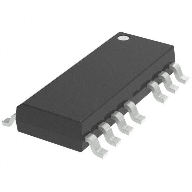
| 描述 | IC SWITCH DUAL SPST SOT23-8 |
| 产品分类 | |
| 品牌 | Intersil |
| 数据手册 | |
| 产品图片 |
|
| 产品型号 | ISL43120IHZ-T |
| rohs | 无铅 / 符合限制有害物质指令(RoHS)规范要求 |
| 产品系列 | - |
| 供应商器件封装 | SOT-23-8 |
| 其它名称 | ISL43120IHZ-DKR |
| 功能 | |
| 包装 | Digi-Reel® |
| 安装类型 | 表面贴装 |
| 导通电阻 | 20 欧姆 |
| 封装/外壳 | SOT-23-8 |
| 工作温度 | -40°C ~ 85°C |
| 标准包装 | 1 |
| 电压-电源,单/双 (±) | 2.7 V ~ 12 V |
| 电压源 | 单电源 |
| 电流-电源 | 1µA |
| 电路 | 2 x SPST - NO |


- 商务部:美国ITC正式对集成电路等产品启动337调查
- 曝三星4nm工艺存在良率问题 高通将骁龙8 Gen1或转产台积电
- 太阳诱电将投资9.5亿元在常州建新厂生产MLCC 预计2023年完工
- 英特尔发布欧洲新工厂建设计划 深化IDM 2.0 战略
- 台积电先进制程称霸业界 有大客户加持明年业绩稳了
- 达到5530亿美元!SIA预计今年全球半导体销售额将创下新高
- 英特尔拟将自动驾驶子公司Mobileye上市 估值或超500亿美元
- 三星加码芯片和SET,合并消费电子和移动部门,撤换高东真等 CEO
- 三星电子宣布重大人事变动 还合并消费电子和移动部门
- 海关总署:前11个月进口集成电路产品价值2.52万亿元 增长14.8%


PDF Datasheet 数据手册内容提取
DATASHEET ISL43120, ISL43121, ISL43122 FN6033 Low-Voltage, Single Supply, Dual SPST Analog Switches Rev 7.00 Aug 17, 2015 The Intersil ISL43120, ISL43121 and ISL43122 devices are Features precision, bidirectional, dual analog SPST switches designed to operate from a single +2.7V to +12V supply. Targeted • Fully specified at 12V, 5V, and 3.3V supplies for 10% applications include battery powered equipment that benefit tolerances from the devices’ low power consumption (5µW), low leakage • ON-resistance (rON) . . . . . . . . . . . . . . . . . . . . . . . . . . . . . . . 19Ω currents (100pA max) and fast switching speeds (tON = 28ns, tOFF = 20ns). Cell phones, for example, often face ASIC • rON matching between channels . . . . . . . . . . . . . . . . . . . . . . . <1Ω functionality limitations. The number of analog input or GPIO • Low charge injection. . . . . . . . . . . . . . . . . . . . . . . . . . . . 5pC (Max) pins may be limited and digital geometries are not well suited to • Single supply operation . . . . . . . . . . . . . . . . . . . . . . +2.7V to +12V analog switch performance. This family of parts may be used to “mux-in” additional functionality while reducing ASIC design • Low power consumption (PD). . . . . . . . . . . . . . . . . . . . . . . . .<5µW risk. Some of the smallest packages are available, alleviating • Low leakage current . . . . . . . . . . . . . . . . . . . . . . . . . . . . . 10nA board space limitations and making Intersil’s newest line of • Fast switching action low-voltage switches an ideal solution. - tON. . . . . . . . . . . . . . . . . . . . . . . . . . . . . . . . . . . . . . . . . . 28ns The ISL43120, ISL43121, ISL43122 are dual - tOFF . . . . . . . . . . . . . . . . . . . . . . . . . . . . . . . . . . . . . . . . . 20ns single-pole/single-throw (SPST) devices. The ISL43120 has • Guaranteed break-before-make (ISL43122 only) two normally open (NO) switches; the ISL43121 has two normally closed (NC) switches; the ISL43122 has one NO and • Minimum 2000V ESD protection per method 3015.7 one NC switch and can be used as an SPDT. • TTL, CMOS compatible TABLE 1. FEATURES AT A GLANCE • Available in SOT-23 packaging ISL43120 ISL43121 ISL43122 • Pb-free (RoHS Compliant) SW 1/SW 2 NO/NO NC/NC NO/NC Applications 3.3V rON 32Ω 32Ω 32Ω • Battery-powered, handheld and portable equipment 3.3V tON/tOFF 40ns/20ns 40ns/20ns 40ns/20ns - Cellular/mobile phones 5V rON 19Ω 19Ω 19Ω - Pagers - Laptops, notebooks, palmtops 5V tON/tOFF 28ns/20ns 28ns/20ns 28ns/20ns • Communications systems 12V rON 11Ω 11Ω 11Ω - Radios, ADSL Modems 12V tON/tOFF 25ns/17ns 25ns/17ns 25ns/17ns - PBX, PABX Packages 8 Ld SOT-23 • Test and measurement equipment - Ultrasound Related Literature - Computerized Tomography (CT) Scanner •TB363 “Guidelines for Handling and Processing Moisture - Magnetic Resonance Image (MRI) Sensitive Surface Mount Devices (SMDs)” - Position Emission Tomography (PET) Scanner •AN557“Recommended Test Procedures for Analog - Electrocardiograph Switches” • Heads-up displays •TB401“Using the ISL43120 SPST Switch in a Multi-Phase • Audio and video switching PWM Power Application” • Various circuits - +3V/+5V DACs and ADCs - Sample and hold circuits - Digital filters - Operational amplifier gain switching networks - High frequency analog switching - High speed multiplexing - Integrator reset circuits FN6033 Rev 7.00 Page 1 of 13 Aug 17, 2015
ISL43120, ISL43121, ISL43122 Ordering Information PART NUMBER PART PACKAGE PKG. (Notes1, 2, 3) MARKING TEMP. RANGE (°C) (RoHS Compliant) DWG. # ISL43120IHZ-T 120Z (Note4) -40 to +85 8 Ld SOT-23 P8.064 ISL43121IHZ-T (No longer available, 121Z (Note4) -40 to +85 8 Ld SOT-23 P8.064 recommended replacement: ISL43120IHZ-T) ISL43122IHZ-T (No longer available, 122Z (Note4) -40 to +85 8 Ld SOT-23 P8.064 recommended replacement: ISL43120IHZ-T) NOTES: 1. Please refer to TB347 for details on reel specifications. 2. These Intersil Pb-free plastic packaged products employ special Pb-free material sets, molding compounds/die attach materials, and 100% matte tin plate plus anneal (e3 termination finish, which is RoHS compliant and compatible with both SnPb and Pb-free soldering operations). Intersil Pb-free products are MSL classified at Pb-free peak reflow temperatures that meet or exceed the Pb-free requirements of IPC/JEDEC J STD-020. 3. For Moisture Sensitivity Level (MSL), please see product information page for ISL43120, ISL43121, ISL43122. For more information on MSL, please see tech brief TB363. 4. The part marking is located on the bottom of the part. Pin Configurations (Note5) ISL43120 ISL43121 ISL43122 (8 LD SOT-23) (8 LD SOT-23) (8 LD SOT-23) TOP VIEW TOP VIEW TOP VIEW NO1 1 8 COM1 NC1 1 8 COM1 NO1 1 8 COM1 V+ 2 7 IN1 V+ 2 7 IN1 V+ 2 7 IN1 IN2 3 6 GND IN2 3 6 GND IN2 3 6 GND COM2 4 5 NO2 COM2 4 5 NC2 COM2 4 5 NC2 NOTE: 5. Switches Shown for Logic “0” Input. Truth Table ISL43120 ISL43121 ISL43122 IN1 IN2 NO1 NO2 NC1 NC2 NO1 NC2 0 0 OFF OFF ON ON OFF ON 0 1 OFF ON ON OFF OFF OFF 1 0 ON OFF OFF ON ON ON 1 1 ON ON OFF OFF ON OFF NOTE: Logic “0” 0.8V. Logic “1” 2.4V. Pin Descriptions ISL43120 ISL43121 ISL43122 PIN NUMBER PIN NUMBER PIN NUMBER PIN NAME FUNCTION 2 2 2 V+ System Power Supply Input (+2.7V to +12V) 6 6 6 GND Ground Connection 3, 7 3, 7 3, 7 INx Digital Control Input 4, 8 4, 8 4, 8 COMx Analog Switch Common Pin 1, 5 1 NOx Analog Switch Normally Open Pin 1, 6 5 NCx Analog Switch Normally Closed Pin FN6033 Rev 7.00 Page 2 of 13 Aug 17, 2015
ISL43120, ISL43121, ISL43122 Absolute Maximum Ratings Thermal Information V+ to GND . . . . . . . . . . . . . . . . . . . . . . . . . . . . . . . . . . . . . . . . . . -0.3V to 15V Thermal Resistance (Typical, Note7) JA (°C/W) Input Voltages 8 Ld SOT-23 Package. . . . . . . . . . . . . . . . . . . . . . . . . . . . 215 IN (Note6). . . . . . . . . . . . . . . . . . . . . . . . . . . . . . . . . . . -0.3V to ((V+) + 0.3V) Maximum Junction Temperature (Plastic Package) . . . . . . . . . . . +150°C NO, NC (Note6). . . . . . . . . . . . . . . . . . . . . . . . . . . . . . . -0.3V to ((V+) + 0.3V) Maximum Storage Temperature Range. . . . . . . . . . . . . . . . . -65°C to +150°C Output Voltages Pb-free Reflow Profile . . . . . . . . . . . . . . . . . . . . . . . . . . . . . . . . . . see TB493 COM (Note6). . . . . . . . . . . . . . . . . . . . . . . . . . . . . . . . . -0.3V to ((V+) + 0.3V) Continuous Current (Any Terminal) . . . . . . . . . . . . . . . . . . . . . . . . . . . 30mA Recommended Operating Conditions Peak Current NO, NC, or COM (Pulsed 1ms, 10% Duty Cycle, Max). . . . . . . . . . . . . . . . . . . . . . . . . . . 40mA Temperature Range. . . . . . . . . . . . . . . . . . . . . . . . . . . . . . . -40°C to +85°C ESD Rating Human Body Model (Per MIL-STD-883 Method 3015) . . . . . . . . . . >2kV CAUTION: Do not operate at or near the maximum ratings listed for extended periods of time. Exposure to such conditions may adversely impact product reliability and result in failures not covered by warranty. NOTES: 6. Signals on NC, NO, COM, or IN exceeding V+ or GND are clamped by internal diodes. Limit forward diode current to maximum current ratings. 7. JA is measured with the component mounted on a low effective thermal conductivity test board in free air. See Tech Brief TB379 for details. Electrical Specifications - 5V Supply V+ = +4.5V to +5.5V, GND = 0V, VINH = 2.4V, VINL = 0.8V (Note8), unless otherwise specified.Boldface limits apply across the operating temperature range, -40°C to +85°C. TEMP MIN MAX PARAMETER TEST CONDITIONS (°C) (Notes9, 10) TYP (Notes9, 10) UNIT ANALOG SWITCH CHARACTERISTICS Analog Signal Range, VANALOG Full 0 - V+ V ON-resistance, rON V+ = 4.5V, ICOM = 1.0mA, VNO or VNC = 3.5V 25 - 19 30 Ω (see Figure5) Full - 23 40 Ω rON Matching Between Channels, V+ = 5V, ICOM = 1.0mA, VNO or VNC = 3.5V 25 - 0.8 2 Ω rON Full - 1 4 Ω rON Flatness, rFLAT(ON) V+ = 5V, ICOM = 1.0mA, VNO or VNC = 1V, 2V, 3V Full - 7 8 Ω NO or NC OFF Leakage Current, V+ = 5.5V, VCOM = 1V, 4.5V, VNO or VNC = 4.5V, 1V 25 -0.1 0.01 0.1 nA INO(OFF) or INC(OFF) Full -5 - 5 nA COM OFF Leakage Current, ICOM(OFF) V+ = 5.5V, VCOM = 4.5V, 1V, VNO or VNC = 1V, 4.5V 25 -0.1 - 0.1 nA Full -5 - 5 nA COM ON Leakage Current, ICOM(ON) V = 5.5V, VCOM = 1V, 4.5V, or VNO or VNC = 1V, 4.5V, or 25 -0.2 - 0.2 nA Floating Full -10 - 10 nA DYNAMIC CHARACTERISTICS Turn-ON Time, tON VNO or VNC = 3V, RL =1kΩ, CL = 35pF, VIN = 0V to 3V 25 - 28 75 ns (seeFigure1, Note11) Full - 40 150 ns Turn-OFF Time, tOFF VNO or VNC = 3V, RL =1kΩ, CL = 35pF, VIN = 0V to 3V 25 - 20 50 ns (seeFigure1, Note11) Full - 30 100 ns Break-Before-Make Time Delay RL = 300Ω, CL = 35pF, VNO = VNC = 3V, VIN = 0V to 3V Full 3 10 - ns (ISL43122 only), tD (seeFigure3, Note11) Charge Injection, Q CL = 1.0nF, VG = 0V, RG = 0 (see Figure2, Note11) 25 - 3 5 pC OFF Isolation RL = 50Ω, CL = 5pF, f = 1MHz (see Figure4) 25 - 76 - dB Crosstalk (Channel-to-Channel) RL = 50Ω, CL = 5pF, f = 1MHz (see Figure6) 25 - -105 - dB Power Supply Rejection Ratio RL = 50Ω, CL = 5pF, f = 1MHz 25 - 60 - dB NO or NC OFF Capacitance, COFF f = 1MHz, VNO or VNC = VCOM = 0V (see Figure7) 25 - 8 - pF COM OFF Capacitance, CCOM(OFF) f = 1MHz, VNO or VNC = VCOM = 0V (see Figure7) 25 - 8 - pF COM ON Capacitance, CCOM(ON) f = 1MHz, VNO or VNC = VCOM = 0V (see Figure7) 25 - 21 - pF FN6033 Rev 7.00 Page 3 of 13 Aug 17, 2015
ISL43120, ISL43121, ISL43122 Electrical Specifications - 5V Supply V+ = +4.5V to +5.5V, GND = 0V, VINH = 2.4V, VINL = 0.8V (Note8), unless otherwise specified.Boldface limits apply across the operating temperature range, -40°C to +85°C. (Continued) TEMP MIN MAX PARAMETER TEST CONDITIONS (°C) (Notes9, 10) TYP (Notes9, 10) UNIT POWER SUPPLY CHARACTERISTICS Power Supply Range Full 2.7 - 12 V Positive Supply Current, I+ V+ = 5.5V, VIN = 0V or V+, all channels on or off Full -1 0.0001 1 µA DIGITAL INPUT CHARACTERISTICS Input Voltage Low, VINL Full - - 0.8 V Input Voltage High, VINH Full 2.4 - - V Input Current, IINH, IINL V+ = 5.5V, VIN = 0V or V+ Full -1 - 1 µA Electrical Specifications - 3.3V Supply V+ = +3.0V to +3.6V, GND = 0V, VINH = 2.4V, VINL = 0.8V (Note8), unless otherwise specified.Boldface limits apply across the operating temperature range, -40°C to +85°C. TEMP MIN MAX PARAMETER TEST CONDITIONS (°C) (Notes9, 10) TYP (Notes9, 10) UNIT ANALOG SWITCH CHARACTERISTICS Analog Signal Range, VANALOG Full 0 - V+ V ON-resistance, rON V+ = 3V, ICOM = 1.0mA, VNO or VNC = 1.5V 25 - 32 50 Ω Full - 40 60 Ω rON Matching Between Channels, V+ = 3.3V, ICOM = 1.0mA, VNO or VNC = 1.5V 25 - 0.8 2 Ω rON Full - 1 4 Ω rON Flatness, rFLAT(ON) V+ = 3.3V, ICOM = 1.0mA, VNO or VNC = 0.5V, 1V, 1.5V 25 - 6 8 Ω Full - 7 12 Ω NO or NC OFF Leakage Current, V+ = 3.6V, VCOM = 1V, 3V, VNO or VNC = 3V, 1V 25 -0.1 0.01 0.1 nA INO(OFF) or INC(OFF) Full -5 - 5 nA COM OFF Leakage Current, ICOM(OFF) V+ = 3.6V, VCOM = 3V, 1V, VNO or VNC = 1V, 3V 25 -0.1 0.01 0.1 nA Full -5 - 5 nA COM ON Leakage Current, ICOM(ON) V = 3.6V, VCOM = 1V, 3V, or VNO or VNC = 1V, 3V, or floating 25 -0.2 - 0.2 nA Full -10 - 10 nA DYNAMIC CHARACTERISTICS Turn-ON Time, tON VNO or VNC = 1.5V, RL = 1kΩ, CL = 35pF, 25 - 40 120 ns VIN = 0V to 3V (Note11) Full - 60 200 ns Turn-OFF Time, tOFF VNO or VNC = 1.5V, RL = 1kΩ, CL = 35pF, 25 - 20 50 ns VIN = 0V to 3V (Note11) Full - 30 120 ns Break-before-make Time Delay RL = 300Ω, CL = 35pF, VNO or VNC = 1.5V, Full 3 20 - ns (ISL43122 only), tD VIN = 0V to 3V (Note11) Charge Injection, Q CL = 1.0nF, VG = 0V, RG = 0ΩNote11) 25 - 1 5 pC OFF-isolation RL = 50Ω, CL = 5pF, f = 1MHz 25 - 76 - dB Crosstalk (Channel-to-channel) RL = 50Ω, CL = 5pF, f = 1MHz 25 - -105 - dB Power Supply Rejection Ratio RL = 50Ω, CL = 5pF, f = 1MHz 25 - 56 - dB NO or NC OFF Capacitance, COFF f = 1MHz, VNO or VNC = VCOM = 0V 25 - 8 - pF COM OFF Capacitance, CCOM(OFF) f = 1MHz, VNO or VNC = VCOM = 0V 25 - 8 - pF COM ON Capacitance, CCOM(ON) f = 1MHz, VNO or VNC = VCOM = 0V (See Figure7) 25 - 21 - pF POWER SUPPLY CHARACTERISTICS Positive Supply Current, I+ V+ = 3.6V, VIN = 0V or V+, all channels on or off Full -1 - 1 µA FN6033 Rev 7.00 Page 4 of 13 Aug 17, 2015
ISL43120, ISL43121, ISL43122 Electrical Specifications - 3.3V Supply V+ = +3.0V to +3.6V, GND = 0V, VINH = 2.4V, VINL = 0.8V (Note8), unless otherwise specified.Boldface limits apply across the operating temperature range, -40°C to +85°C. (Continued) TEMP MIN MAX PARAMETER TEST CONDITIONS (°C) (Notes9, 10) TYP (Notes9, 10) UNIT DIGITAL INPUT CHARACTERISTICS Input Voltage Low, VINL Full - - 0.8 V Input Voltage High, VINH Full 2.4 - - V Input Current, IINH, IINL V+ = 3.6V, VIN = 0V or V+ Full -1 - 1 µA Electrical Specifications - 12V Supply V+ = +10.8V to +13V, GND = 0V, VINH = 2.4V, VINL = 0.8V (Note8), unless otherwise specified.Boldface limits apply across the operating temperature range, -40°C to +85°C. TEMP MIN MAX PARAMETER TEST CONDITIONS (°C) (Notes9, 10) TYP (Notes9, 10) UNIT ANALOG SWITCH CHARACTERISTICS Analog Signal Range, VANALOG Full 0 - V+ V ON-resistance, rON V+ = 10.8V, ICOM = 1.0mA, VNO or VNC = 10V 25 - 11 20 Ω Full - 15 25 Ω rON Matching Between Channels, rON V+ = 12V, ICOM = 1.0mA, VNO or VNC = 10V 25 - 0.8 2 Ω Full - 1 4 Ω rON Flatness, rFLAT(ON) V+ = 12V, ICOM = 1.0mA, VNO or VNC = 3V, 6V, 9V 25 - 1 4 Ω Full - - 6 Ω NO or NC OFF Leakage Current, V+ = 13V, VCOM = 1V, 12V, VNO or VNC = 12V, 1V 25 -0.1 0.01 0.1 nA INO(OFF) or INC(OFF) Full -5 - 5 nA COM OFF Leakage Current, ICOM(OFF) V+ = 13V, VCOM = 12V, 1V, VNO or VNC = 1V, 12V 25 -0.1 0.01 0.1 nA Full -5 - 5 nA COM ON Leakage Current, ICOM(ON) V = 13V, VCOM = 1V, 12V, or VNO or VNC = 1V, 12V, or 25 -0.2 - 0.2 nA floating Full -10 - 10 nA DYNAMIC CHARACTERISTICS Turn-ON Time, tON VNO or VNC = 10V, RL = 1kΩ, CL = 35pF, VIN = 0V to 4V 25 - 25 35 ns (Note11) Full - 35 55 ns Turn-OFF Time, tOFF VNO or VNC = 10V, RL = 1kΩ, CL = 35pF, VIN = 0V to 4V 25 - 17 30 ns (Note11) Full - 26 50 ns Break-before-make Time Delay RL = 300Ω, CL = 35pF, VNO or VNC = 10V, Full 0 2 ns (ISL43122 only), tD VIN = 0 to 4V Charge Injection, Q CL = 1.0nF, VG = 0V, RG = 0(Note11) 25 - 5 15 pC OFF-isolation RL = 50Ω, CL = 5pF, f = 1MHz 25 - 76 - dB Crosstalk (Channel-to-channel) RL = 50Ω, CL = 5pF, f = 1MHz 25 - -105 - dB Power Supply Rejection Ratio RL = 50Ω, CL = 5pF, f = 1MHz 25 - 63 - dB NO or NC OFF Capacitance, COFF f = 1MHz, VNO or VNC = VCOM = 0V 25 - 8 - pF COM OFF Capacitance, CCOM(OFF) f = 1MHz, VNO or VNC = VCOM = 0V 25 - 8 - pF COM ON Capacitance, CCOM(ON) f = 1MHz, VNO or VNC = VCOM = 0V (see Figure7) 25 - 21 - pF POWER SUPPLY CHARACTERISTICS Positive Supply Current, I+ V+ = 13V, VIN = 0V or V+, all channels on or off Full -1 - 1 µA FN6033 Rev 7.00 Page 5 of 13 Aug 17, 2015
ISL43120, ISL43121, ISL43122 Electrical Specifications - 12V Supply V+ = +10.8V to +13V, GND = 0V, VINH = 2.4V, VINL = 0.8V (Note8), unless otherwise specified.Boldface limits apply across the operating temperature range, -40°C to +85°C. (Continued) TEMP MIN MAX PARAMETER TEST CONDITIONS (°C) (Notes9, 10) TYP (Notes9, 10) UNIT DIGITAL INPUT CHARACTERISTICS Input Voltage Low, VINL Full - - 0.8 V Input Voltage High, VINH Full 4 - - V Input Current, IINH, IINL V+ = 13V, VIN = 0V or V+ Full -1 - 1 µA NOTES: 8. VIN = input voltage to perform proper function. 9. The algebraic convention, whereby the most negative value is a minimum and the most positive a maximum, is used in this data sheet. 10. Compliance to datasheet limits is assured by one or more methods: production test, characterization and/or design. 11. Limits established by characterization and are not production tested. Test Circuits and Waveforms 3V OR 4V tr < 20ns V+ C LOGIC 50% tf < 20ns INPUT 0V tOFF NO OR NC VOUT SWITCH SWITCH INPUT COM INPUT VNO VOUT IN 90% 90% SWITCH LOGIC GND RL CL OUTPUT 0V INPUT 1k 35pF tON Logic input waveform is inverted for switches that have the opposite Repeat test for all switches. CL includes fixture and stray logic sense. capacitance. R L V = V ------------------------ OUT (NO or NC) R +r L ON FIGURE 1A. MEASUREMENT POINTS FIGURE 1B. TEST CIRCUIT FIGURE 1. SWITCHING TIMES V+ C OSUWTITPCUHT VOUT RG NO OR NC COM VOUT VOUT V+ LINOPGUICT ON OFF ON VG GND IN CL 0V LOGIC INPUT Q = VOUT x CL FIGURE 2A. MEASUREMENT POINTS FIGURE 2B. TEST CIRCUIT FIGURE 2. CHARGE INJECTION FN6033 Rev 7.00 Page 6 of 13 Aug 17, 2015
ISL43120, ISL43121, ISL43122 Test Circuits and Waveforms (Continued) V+ C 3V OR 4V LOGIC INPUT 0V NO1 VOUT1 VNX COM1 NC2 VOUT2 RL1 CL1 SWITCH 90% COM2 300Ω 35pF OUTPUT IN1 VOUT1 0V RL2 CL2 300Ω 35pF IN2 SWITCH 90% OUVTOPUUTT2 0V LINOPGUICT GND tD tD CL includes fixture and stray capacitance. FIGURE 3A. MEASUREMENT POINTS (ISL43122 ONLY) FIGURE 3B. TEST CIRCUIT (ISL43122 ONLY) FIGURE 3. BREAK-BEFORE-MAKE TIME V+ V+ C C rON = V1/1mA SIGNAL GENERATOR NO OR NC NO OR NC VNX INX 0V OR VINH 1mA V1 IN 0.8V OR VINH COM COM ANALYZER GND GND RL FIGURE 4. OFF-ISOLATION TEST CIRCUIT FIGURE 5. rON TEST CIRCUIT V+ C V+ C SIGNAL GENERATOR NO1 OR NC1 COM1 50 NO OR NC IN1 0V OR 2.4V IN2 0V OR VINH IMPEDANCE INX 0V OR VINH ANALYZER COM2 NO2 OR NC2 COM ANALYZER NC GND GND RL FIGURE 6. CROSSTALK TEST CIRCUIT FIGURE 7. CAPACITANCE TEST CIRCUIT FN6033 Rev 7.00 Page 7 of 13 Aug 17, 2015
ISL43120, ISL43121, ISL43122 Detailed Description Power-Supply Considerations The ISL43120, ISL43121, ISL43122 construction is typical of The ISL43120, ISL43121, ISL43122 bidirectional dual SPST most CMOS analog switches, except that they have only two analog switches offer precise switching capability from a supply pins: V+ and GND. V+ and GND drive the internal CMOS single 2.7V to 12V supply with low ON-resistance (19Ω) and switches and set their analog voltage limits. Unlike switches high speed operation (tON=28ns, tOFF = 20ns). The devices with a 13V maximum supply voltage, the ISL43120, are especially well suited to portable battery-powered ISL43121, ISL43122 15V maximum supply voltage provides equipment thanks to the low operating supply voltage (2.7V), plenty of room for the 10% tolerance of 12V supplies, as well low power consumption (5µW), low leakage currents as room for overshoot and noise spikes. (100pAmax), and the tiny SOT-23 packaging. High frequency applications also benefit from the wide bandwidth, and the very The minimum recommended supply voltage is 2.7V. It is high off-isolation and crosstalk rejection. important to note that the input signal range, switching times, and ON-resistance degrade at lower supply voltages. Refer to Supply Sequencing and Overvoltage the “Electrical Specifications” tables starting on page3 and Protection “Typical Performance Curves” (starting on page9) for details. With any CMOS device, proper power supply sequencing is V+ and GND also power the internal logic and level shifter. The required to protect the device from excessive input currents, level shifter convert the input logic levels to switched V+ and which might permanently damage the IC. All I/O pins contain GND signals to drive the analog switch gate terminals. ESD protection diodes from the pin to V+ and GND This family of switches cannot be operated with bipolar (seeFigure8). To prevent forward biasing these diodes, V+ supplies, because the input switching point becomes negative must be applied before any input signals, and input signal in this configuration. voltages must remain between V+ and GND. If these conditions cannot be guaranteed, then one of the following Logic-level Thresholds two protection methods should be employed. This switch family is TTL compatible (0.8V and 2.4V) over a Logic inputs can easily be protected by adding a 1kΩ resistor in supply range of 3V to 11V (see Figure15). At 12V the VIH level series with the input (see Figure8). The resistor limits the input is about 2.5V. This is still below the TTL guaranteed high output current below the threshold that produces permanent minimum level of 2.8V, but noise margin is reduced. For best damage, and the sub-microamp input current produces an results with a 12V supply, use a logic family the provides a VOH insignificant voltage drop during normal operation. greater than 3V. Adding a series resistor to the switch input defeats the purpose The digital input stages draw supply current whenever the of using a low rON switch, so two small signal diodes can be digital input voltage is not at one of the supply rails. Driving the added in series with the supply pins to provide overvoltage digital input signals from GND to V+ with a fast transition time protection for all pins (see Figure8). These additional diodes minimizes power dissipation. limit the analog signal from 1V below V+ to 1V above GND. The low leakage current performance is unaffected by this High-frequency Performance approach, but the switch resistance may increase, especially In 50Ω systems, signal response is reasonably flat even past at low supply voltages. 300MHz (see Figure16). Figure 16 also illustrates that the frequency response is very consistent over a wide V+ range, and for varying analog signal levels. OPTIONAL PROTECTION DIODE An OFF switch acts like a capacitor and passes higher frequencies with less attenuation, resulting in signal V+ OPTIONAL feedthrough from a switch’s input to its output. Off-isolation is PROTECTION the resistance to this feedthrough, while crosstalk indicates RESISTOR INX the amount of feedthrough from one switch to another. Figure17 details the high off-isolation and crosstalk rejection VNO OR NC VCOM provided by this family. At 10MHz, off isolation is about 50dB in 50Ω systems, decreasing approximately 20dB per decade as frequency increases. Higher load impedances decrease off GND isolation and crosstalk rejection due to the voltage divider OPTIONAL PROTECTION action of the switch OFF impedance and the load impedance. DIODE FIGURE 8. OVERVOLTAGE PROTECTION FN6033 Rev 7.00 Page 8 of 13 Aug 17, 2015
ISL43120, ISL43121, ISL43122 Leakage Considerations signal varies. The difference in the two diode leakages to the V+ and GND pins constitutes the analog-signal-path leakage current. Reverse ESD protection diodes are internally connected between All analog leakage current flows between each pin and one of the each analog-signal pin and both V+ and GND. One of these diodes supply terminals, not to the other switch terminal. This is why both conducts if any analog signal exceeds V+ or GND. sides of a given switch can show leakage currents of the same or Virtually all the analog leakage current comes from the ESD opposite polarity. There is no connection between the analog diodes to V+ or GND. Although the ESD diodes on a given signal signal paths and V+ or GND. pin are identical and therefore fairly well balanced, they are reverse biased differently. Each is biased by either V+ or GND and the analog signal. This means their leakages will vary as the Typical Performance Curves TA = +25°C, unless otherwise specified. 40 45 V+ = 3.3V 40 35 35 30 +85°C 30 25 +85°C 20 +25°C -40°C 25 15 Ω ()ON 20 Ω ()N 2350 V+ = 5V r O 20 +85°C r 15 +25°C 15 +25°C 10 -40°C 20 -40°C +85°C V+ = 12V 10 15 +25°C 10 5 5 -40°C 3 4 5 6 7 8 9 10 11 12 13 0 2 4 6 8 10 12 V+ (V) VCOM (V) FIGURE 9. ON-RESISTANCE vs SUPPLY VOLTAGE FIGURE 10. ON-RESISTANCE vs SWITCH VOLTAGE 0.50 60 V+ = 3.3V 0.40 +25°C 0.30 50 0.20 0.10 +85°C 40 -40°C 0 0.25 30 V+ = 5V 0.20 Ω ()ON 00..1105 +25°C +85°C Q (pC) 20 V+ = 5V V+ = 12V r 0.05 +85°C 10 -40°C V+ = 3.3V 0 0.15 0 +25°C V+ = 12V 0.10 -40°C +85°C -10 0.05 -40°C +25°C 0 -20 0 2 4 6 8 10 12 0 2 4 6 8 10 12 VCOM (V) VCOM (V) FIGURE 11. rON MATCH vs SWITCH VOLTAGE FIGURE 12. CHARGE INJECTION vs SWITCH VOLTAGE FN6033 Rev 7.00 Page 9 of 13 Aug 17, 2015
ISL43120, ISL43121, ISL43122 Typical Performance Curves TA = +25°C, unless otherwise specified. (Continued) 100 35 90 80 30 +85°C 70 s) ns) (nN 60 (FF25 O +85°C O t t 50 -40°C -40°C 40 20 -40°C 30 +25°C 25°C 20 15 2 3 4 5 6 7 8 9 10 11 12 2 3 4 5 6 7 8 9 10 11 12 V+ (V) V+ (V) FIGURE 13. TURN-ON TIME vs SUPPLY VOLTAGE FIGURE 14. TURN-OFF TIME vs SUPPLY VOLTAGE 3.0 B) d V+ = 3.3V TO 12V AIN ( 0 GAIN G 2.5 D -3 VINH ZE LI-6 (V)NL2.0 -40°C +85°C ORMA PHASE 0 VI N D 20 ANH1.5 +25°C +85°C 40 VIN -40°C 60 E (°) S +25°C A 1.0 RL = 50 80 H VINL VIN = 0.2VP-P TO 2.5VP-P (V+ = 3.3V) P +85°C VIN = 0.2VP-P TO 4VP-P (V+ = 5V) 100 VIN = 0.2VP-P TO 5VP-P (V+ = 12V) 0.5 2 3 4 5 6 7 8 9 10 11 12 13 1M 10M 100M 600M V+ (V) FREQUENCY (Hz) FIGURE 15. DIGITAL SWITCHING POINT vs SUPPLY VOLTAGE FIGURE 16. FREQUENCY RESPONSE FN6033 Rev 7.00 Page 10 of 13 Aug 17, 2015
ISL43120, ISL43121, ISL43122 Typical Performance Curves TA = +25°C, unless otherwise specified. (Continued) -10 10 V+ = 3V TO 13V RL = 50 -20 20 0 -30 30 10 V+ = 3.3V, SWITCH OFF -40 40 20 B) dB) V+ = 12V, SWITCH OFF K (d-50 50 ON ( dB) 30 ROSSTAL--6700 ISOLATION 6700 F ISOLATI ±PSRR ( 4500 V+ = 12V, SWITCH ON C F -80 80 O 60 V+ = 3.3V, SWITCH ON -90 90 70 CROSSTALK -100 100 80 -110 110 1k 10k 100k 1M 10M 100M 500M 0.3k 1M 10M 100M 1G FREQUENCY (Hz) FREQUENCY (Hz) FIGURE 17. CROSSTALK AND OFF-ISOLATION FIGURE 18. ±PSRR vs FREQUENCY Die Characteristics SUBSTRATE POTENTIAL (POWERED UP): GND TRANSISTOR COUNT: ISL43120: 66 ISL43121: 66 ISL43122: 66 PROCESS: Si Gate CMOS FN6033 Rev 7.00 Page 11 of 13 Aug 17, 2015
ISL43120, ISL43121, ISL43122 Revision History The revision history provided is for informational purposes only and is believed to be accurate, but not warranted. Please go to the web to make sure that you have the latest revision. DATE REVISION CHANGE August 17, 2015 FN6033.7 Updated Ordering Information table on page2. May 28, 2015 FN6033.6 Added Rev History beginning with Rev 6. Updated entire datasheet applying Intersil’s new standards. Updated Ordering information by removing obsolete parts, adding MSL and part marking notes. About Intersil Intersil Corporation is a leading provider of innovative power management and precision analog solutions. The company's products address some of the largest markets within the industrial and infrastructure, mobile computing and high-end consumer markets. For the most updated datasheet, application notes, related documentation and related parts, please see the respective product information page found at www.intersil.com. You may report errors or suggestions for improving this datasheet by visiting www.intersil.com/ask. Reliability reports are also available from our website at www.intersil.com/support © Copyright Intersil Americas LLC 2003-2015. All Rights Reserved. All trademarks and registered trademarks are the property of their respective owners. For additional products, see www.intersil.com/en/products.html Intersil products are manufactured, assembled and tested utilizing ISO9001 quality systems as noted in the quality certifications found at www.intersil.com/en/support/qualandreliability.html Intersil products are sold by description only. Intersil may modify the circuit design and/or specifications of products at any time without notice, provided that such modification does not, in Intersil's sole judgment, affect the form, fit or function of the product. Accordingly, the reader is cautioned to verify that datasheets are current before placing orders. Information furnished by Intersil is believed to be accurate and reliable. However, no responsibility is assumed by Intersil or its subsidiaries for its use; nor for any infringements of patents or other rights of third parties which may result from its use. No license is granted by implication or otherwise under any patent or patent rights of Intersil or its subsidiaries. For information regarding Intersil Corporation and its products, see www.intersil.com FN6033 Rev 7.00 Page 12 of 13 Aug 17, 2015
ISL43120, ISL43121, ISL43122 Small Outline Transistor Plastic Packages (SOT23-8) P8.064 0.20 (0.008) M C VIEW C 8 LEAD SMALL OUTLINE TRANSISTOR PLASTIC PACKAGE CL e INCHES MILLIMETERS b SYMBOL MIN MAX MIN MAX NOTES A 0.036 0.057 0.90 1.45 - 8 7 6 5 A1 0.000 0.0059 0.00 0.15 - CL E CL E1 A2 0.036 0.051 0.90 1.30 - b 0.009 0.015 0.22 0.38 - 1 2 3 4 b1 0.009 0.013 0.22 0.33 c 0.003 0.009 0.08 0.22 6 e1 c1 0.003 0.008 0.08 0.20 6 D C D 0.111 0.118 2.80 3.00 3 CL E 0.103 0.118 2.60 3.00 - E1 0.060 0.067 1.50 1.70 3 A A2 A1 SPELAATNINEG e 0.0256 Ref 0.65 Ref - e1 0.0768 Ref 1.95 Ref - -C- L 0.014 0.022 0.35 0.55 4 L1 0.024 Ref. 0.60 Ref. 0.10 (0.004) C L2 0.010 Ref. 0.25 Ref. N 8 8 5 WITH b R 0.004 - 0.10 - PLATING b1 R1 0.004 0.010 0.10 0.25 0o 8o 0o 8o - c c1 Rev. 2 9/03 NOTES: BASE METAL 1. Dimensioning and tolerance per ASME Y14.5M-1994. 2. Package conforms to EIAJ SC-74 and JEDEC MO178BA. 4X 1 3. Dimensions D and E1 are exclusive of mold flash, protrusions, or gate burrs. R1 4. Footlength L measured at reference to gauge plane. 5. “N” is the number of terminal positions. R 6. These Dimensions apply to the flat section of the lead between 0.08mm and 0.15mm from the lead tip. GAUGE PLANE SEATING 7. Controlling dimension: MILLIMETER. Converted inch dimensions L PLANE are for reference only C L1 L2 4X 1 VIEW C FN6033 Rev 7.00 Page 13 of 13 Aug 17, 2015