ICGOO在线商城 > 集成电路(IC) > 接口 - 驱动器,接收器,收发器 > ISL4270EIRZ-T
 Datasheet下载
- 型号: ISL4270EIRZ-T
- 制造商: Intersil
- 库位|库存: xxxx|xxxx
- 要求:
| 数量阶梯 | 香港交货 | 国内含税 |
| +xxxx | $xxxx | ¥xxxx |
查看当月历史价格
查看今年历史价格
ISL4270EIRZ-T产品简介:
ICGOO电子元器件商城为您提供ISL4270EIRZ-T由Intersil设计生产,在icgoo商城现货销售,并且可以通过原厂、代理商等渠道进行代购。 ISL4270EIRZ-T价格参考。IntersilISL4270EIRZ-T封装/规格:接口 - 驱动器,接收器,收发器, 全 收发器 3/3 RS232 32-QFN(5x5)。您可以下载ISL4270EIRZ-T参考资料、Datasheet数据手册功能说明书,资料中有ISL4270EIRZ-T 详细功能的应用电路图电压和使用方法及教程。
ISL4270EIRZ-T 是瑞萨电子(Renesas Electronics America Inc.)生产的一款接口器件,属于驱动器、接收器、收发器类别。该芯片主要应用于工业自动化、通信设备和嵌入式系统中,适用于需要可靠数据传输的场合。

ISL4270EIRZ-T 是一款低功耗、高速的RS-422/RS-485收发器,支持全双工和半双工通信。其典型应用场景包括工业控制网络、现场总线系统、楼宇自动化、电机控制以及远程数据采集系统。由于其具备高抗噪能力和稳定的差分信号传输性能,适用于电磁干扰较强的工业环境。

此外,该器件广泛用于PLC(可编程逻辑控制器)、HMI(人机界面)、智能传感器和自动化测试设备中,支持长距离、高速的数据通信,提升了系统间的数据交互效率和稳定性。

其封装形式为TSSOP,适合嵌入在紧凑型PCB设计中,广泛应用于需要高效、可靠通信接口的工业与通信设备中。
| 参数 | 数值 |
| 产品目录 | 集成电路 (IC) |
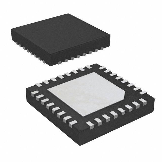
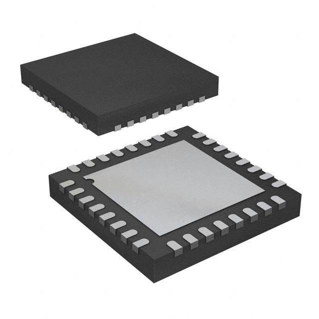
| 描述 | IC XMITTER/RCVR ESD RS232 32-QFN |
| 产品分类 | |
| 品牌 | Intersil |
| 数据手册 | |
| 产品图片 |
|
| 产品型号 | ISL4270EIRZ-T |
| rohs | 无铅 / 符合限制有害物质指令(RoHS)规范要求 |
| 产品系列 | - |
| 产品目录页面 | |
| 供应商器件封装 | 32-QFN(5x5) |
| 其它名称 | ISL4270EIRZ-TDKR |
| 包装 | Digi-Reel® |
| 协议 | RS232 |
| 双工 | 全 |
| 安装类型 | 表面贴装 |
| 封装/外壳 | 32-VFQFN 裸露焊盘 |
| 工作温度 | -40°C ~ 85°C |
| 接收器滞后 | 500mV |
| 数据速率 | 250kbps |
| 标准包装 | 1 |
| 电压-电源 | 3 V ~ 5.5 V |
| 类型 | 收发器 |
| 驱动器/接收器数 | 3/3 |


- 商务部:美国ITC正式对集成电路等产品启动337调查
- 曝三星4nm工艺存在良率问题 高通将骁龙8 Gen1或转产台积电
- 太阳诱电将投资9.5亿元在常州建新厂生产MLCC 预计2023年完工
- 英特尔发布欧洲新工厂建设计划 深化IDM 2.0 战略
- 台积电先进制程称霸业界 有大客户加持明年业绩稳了
- 达到5530亿美元!SIA预计今年全球半导体销售额将创下新高
- 英特尔拟将自动驾驶子公司Mobileye上市 估值或超500亿美元
- 三星加码芯片和SET,合并消费电子和移动部门,撤换高东真等 CEO
- 三星电子宣布重大人事变动 还合并消费电子和移动部门
- 海关总署:前11个月进口集成电路产品价值2.52万亿元 增长14.8%


PDF Datasheet 数据手册内容提取
DATASHEET ISL4270E FN6041 QFN Packaged, ±15kV ESD Protected, +3V to +5.5V, 300nA, 250kbps, RS-232 Rev 2.00 Transceivers with Enhanced Automatic Powerdown and a Separate Logic Supply June 16, 2010 The Intersil ISL4270E is a 3.0V to 5.5V powered RS-232 Features transceiver which meets ElA/TIA-232 and V.28/V.24 • Available in Near Chip Scale QFN (5mmx5mm) Package specifications, even at VCC=3.0V. Additionally, it provides 15kV ESD protection (IEC61000-4-2 Air Gap and Human • VL Supply Pin for Compatibility with Mixed Voltage Body Model) on transmitter outputs and receiver inputs Systems (RS-232 pins). Targeted applications are PDAs, Palmtops, • ESD Protection for RS-232 I/O Pins to 15kV (IEC61000) and notebook and laptop computers where the low operational, and even lower standby power consumption is • Manual and Enhanced Automatic Powerdown Features critical. Efficient on-chip charge pumps, coupled with manual • Meets EIA/TIA-232 and V.28/V.24 Specifications at 3V and enhanced automatic powerdown functions, reduce the • On-Chip Charge Pumps Require Only Four External standby supply current to a 300nA trickle. Tiny 5mmx5mm 0.1F Capacitors Quad Flat No-Lead (QFN) packaging, and the use of small, low value capacitors ensure board space savings as well. • Receivers Stay Active in Powerdown Data rates greater than 250kbps are guaranteed at worst • Very Low Supply Current. . . . . . . . . . . . . . . . . . . . 300A case load conditions. • Guaranteed Minimum Data Rate. . . . . . . . . . . . . 250kbps The ISL4270E features a VL pin that adjusts the logic pin output levels and input thresholds to values compatible with • Wide Power Supply Range . . . . . . . Single +3V to +5.5V the VCC powering the external logic (e.g., a UART). • Low Supply Current in Powerdown State. . . . . . . . 300nA This device includes an enhanced automatic powerdown • Pb-Free (RoHS Compliant) function which powers down the on-chip power-supply and Applications driver circuits. This occurs when all receiver and transmitter inputs detect no signal transitions for a period of 30 seconds. • Any System Requiring RS-232 Communication Ports It power back up, automatically, whenever it senses a - Battery Powered, Hand-Held, and Portable Equipment transition on any transmitter or receiver input. - Laptop Computers, Notebooks, Palmtops Table 1 summarizes the features of the ISL4270E, while - Digital Cameras Application Note AN9863 summarizes the features of each - PDA’s and PDA Cradles device comprising the 3V RS-232 family. - Cellular/Mobile Phones Ordering Information TEMP. PART NUMBER PART RANGE PKG. (Note) MARKING (°C) PACKAGE DWG. # ISL4270EIRZ* ISL4270 EIRZ -40 to +85 32 Ld QFN L32.5x5B (Pb-free) *Add “-T” suffix for tape and reel. Please refer to TB347 for details on reel specifications. NOTE: These Intersil Pb-free plastic packaged products employ special Pb-free material sets, molding compounds/die attach materials, and 100% matte tin plate plus anneal (e3 termination finish, which is RoHS compliant and compatible with both SnPb and Pb-free soldering operations). Intersil Pb-free products are MSL classified at Pb-free peak reflow temperatures that meet or exceed the Pb-free requirements of IPC/JEDEC J STD-020. TABLE 1. SUMMARY OF FEATURES NO. OF NO. OF DATA RATE Rx. ENABLE VL LOGIC MANUAL ENHANCED AUTOMATIC PART NUMBER Tx. Rx. (kbps) FUNCTION? SUPPLY PIN? POWER- DOWN? POWERDOWN FUNCTION? ISL4270E 3 3 250 NO YES YES YES FN6041 Rev 2.00 Page 1 of 13 June 16, 2010
ISL4270E Pinout ISL4270E (QFN) TOP VIEW F F O E C C 1- + 1+ OR CC ND C N C V C F V G N 32 31 30 29 28 27 26 25 NC 1 24 NC C2+ 2 23 T1OUT C2- 3 22 T2OUT V- 4 21 T3OUT PD T1IN 5 20 R1IN T2IN 6 19 R2IN INVALID 7 18 R3IN NC 8 17 NC 9 10 11 12 13 14 15 16 NC T3IN RCEON R3OUT R2OUT R1OUT VL NC O F Pin Descriptions PIN FUNCTION VCC System power supply input (3.0V to 5.5V). V+ Internally generated positive transmitter supply (+5.5V). V- Internally generated negative transmitter supply (-5.5V). GND Ground connection. This is also the potential of the thermal pad (PD). C1+ External capacitor (voltage doubler) is connected to this lead. C1- External capacitor (voltage doubler) is connected to this lead. C2+ External capacitor (voltage inverter) is connected to this lead. C2- External capacitor (voltage inverter) is connected to this lead. TIN TTL/CMOS compatible transmitter Inputs. The switching point is a function of the VL voltage. TOUT 15kV ESD Protected, RS-232 level (nominally 5.5V) transmitter outputs. RIN 15kV ESD Protected, RS-232 compatible receiver inputs. ROUT TTL/CMOS level receiver outputs. Swings between GND and VL. VL Logic-Level Supply. All TTL/CMOS inputs and outputs are powered by this supply. INVALID Active low output that indicates if no valid RS-232 levels are present on any receiver input. Swings between GND and VL. FORCEOFF Active low to shut down transmitters and on-chip power supply. This overrides any automatic circuitry and FORCEON (see Table2). The switching point is a function of the VL voltage. FORCEON Active high input to override automatic powerdown circuitry thereby keeping transmitters active (FORCEOFF must be high). The switching point is a function of the VL voltage. PD Exposed Thermal Pad. Connect to GND. FN6041 Rev 2.00 Page 2 of 13 June 16, 2010
ISL4270E Typical Operating Circuit +3.3V + 0.1F 27 29 0.1CF1 +31 C1+ VCC V+ 30 +0C.31F C1- C2 2 C2+ 0.1F + 3 V- 4 C4 C2- 0.1F + 5 T1 23 T1IN T1OUT T2IN 6 T2 22 T2OUT RS-232 LEVELS 10 T3 21 T3IN T3OUT TTL/CMOS R1 LOGIC LEVELS 14 20 R1OUT R1IN 5k R2 13 19 R2OUT R2IN RS-232 LEVELS 5k 12 R3 18 R3OUT R3IN 5k 15 VL LOGIC VCC + 0.1F 11 FORCEON 28 VCC FORCEOFF TO POWER 7 INVALID GND CONTROL LOGIC 26 FN6041 Rev 2.00 Page 3 of 13 June 16, 2010
ISL4270E Absolute Maximum Ratings Thermal Information VCC to Ground. . . . . . . . . . . . . . . . . . . . . . . . . . . . . . . . -0.3V to 6V Thermal Resistance (Typical, Notes 1, 2) JA (°C/W) JC (°C/W) VL to Ground . . . . . . . . . . . . . . . . . . . . . . . . . . . . . . . . . -0.3V to 7V 32 Ld QFN Package. . . . . . . . . . . . . . . 30 2.2 V+ to Ground. . . . . . . . . . . . . . . . . . . . . . . . . . . . . . . . . -0.3V to 7V Moisture Sensitivity (see Technical Brief TB363) V- to Ground. . . . . . . . . . . . . . . . . . . . . . . . . . . . . . . . . +0.3V to -7V QFN Package. . . . . . . . . . . . . . . . . . . . . . . . . . . . . . . . . . . Level 1 V+ to V- . . . . . . . . . . . . . . . . . . . . . . . . . . . . . . . . . . . . . . . . . . . 14V Maximum Junction Temperature (Plastic Package) . . . . . . . 150oC Input Voltages Maximum Storage Temperature Range. . . . . . . . . . -65oC to 150oC TIN, FORCEON, FORCEOFF . . . . . . . . . . . . . . . . . . -0.3V to 6V Pb-Free Reflow Profile. . . . . . . . . . . . . . . . . . . . . . . . .see link below RIN. . . . . . . . . . . . . . . . . . . . . . . . . . . . . . . . . . . . . . . . . . . . 25V http://www.intersil.com/pbfree/Pb-FreeReflow.asp Output Voltages TOUT . . . . . . . . . . . . . . . . . . . . . . . . . . . . . . . . . . . . . . . . . 13.2V Operating Conditions ShRoOrt UCTi,r cINuiVt ADLuIrDa.t io. n. . . . . . . . . . . . . . . . . . . . . . -0.3V to (VL +0.3V) Temperature Range. . . . . . . . . . . . . . . . . . . . . . . . . . -40oC to 85oC TOUT . . . . . . . . . . . . . . . . . . . . . . . . . . . . . . . . . . . . . Continuous ESD Rating . . . . . . . . . . . . See “ESD PERFORMANCE” on page5 CAUTION: Do not operate at or near the maximum ratings listed for extended periods of time. Exposure to such conditions may adversely impact product reliability and result in failures not covered by warranty. NOTES: 1. JA is measured in free air with the component mounted on a high effective thermal conductivity test board with “direct attach” features. See Tech Brief TB379, and Tech Brief TB389. 2. For JC, the “case temp” location is the center of the exposed metal pad on the package underside. Electrical Specifications Test Conditions: VCC = 3V to 5.5V, C1 - C4 = 0.1µF, VL = VCC; Unless Otherwise Specified. Typicals are at TA = 25oC, VCC = VL = 3.3V TEMP MIN MAX PARAMETER TEST CONDITIONS (oC) (Note 4) TYP (Note 4) UNITS DC CHARACTERISTICS Supply Current, Automatic All RIN Open, FORCEON=GND, FORCEOFF=VCC 25 - 0.3 5 A Powerdown Supply Current, Powerdown FORCEOFF=GND 25 - 0.3 5 A Supply Current, All Outputs Unloaded, FORCEON=FORCEOFF=VCC, 25 - 0.3 1 mA Automatic Powerdown Disabled VCC=3.15V LOGIC AND TRANSMITTER INPUTS Input Logic Threshold Low TIN, FORCEON, FORCEOFF VL = 3.3V or 5V Full - - 0.8 V VL = 2.5V Full - - 0.6 V Input Logic Threshold High TIN, FORCEON, FORCEOFF VL = 5V Full 2.4 - - V VL = 3.3V Full 2.0 - - V VL = 2.5V Full 1.4 - - V VL = 1.8V 25 - 0.9 - V Transmitter Input Hysteresis 25 - 0.5 - V Input Leakage Current TIN, FORCEON, FORCEOFF Full - 0.01 1.0 A RECEIVER OUTPUTS Output Voltage Low IOUT = 1.6mA Full - - 0.4 V Output Voltage High IOUT = -1.0mA Full VL - 0.6 VL - 0.1 - V RECEIVER INPUTS Input Voltage Range Full -25 - 25 V Input Threshold Low VCC = VL = 5.0V 25 0.8 1.5 - V VCC = VL = 3.3V 25 0.6 1.2 - V Input Threshold High VCC = VL = 5.0V 25 - 1.8 2.4 V VCC = VL = 3.3V 25 - 1.5 2.4 V Input Hysteresis 25 - 0.5 - V Input Resistance 25 3 5 7 k FN6041 Rev 2.00 Page 4 of 13 June 16, 2010
ISL4270E Electrical Specifications Test Conditions: VCC = 3V to 5.5V, C1 - C4 = 0.1µF, VL = VCC; Unless Otherwise Specified. Typicals are at TA = 25oC, VCC = VL = 3.3V (Continued) TEMP MIN MAX PARAMETER TEST CONDITIONS (oC) (Note 4) TYP (Note 4) UNITS TRANSMITTER OUTPUTS Output Voltage Swing All Transmitter Outputs Loaded with 3k to Ground Full 5.0 5.4 - V Output Resistance VCC=V+=V-=0V, Transmitter Output=2V Full 300 10M - Output Short-Circuit Current VOUT = 0V Full - 35 60 mA Output Leakage Current VOUT=12V, VCC=0V or 3V to 5.5V Full - - 25 A Automatic Powerdown or FORCEOFF=GND ENHANCED AUTOMATIC POWERDOWN (FORCEON = GND, FORCEOFF = VCC) Receiver Input Thresholds to See Figure 4 Full -2.7 - 2.7 V INVALID High Receiver Input Thresholds to See Figure 4 Full -0.3 - 0.3 V INVALID Low INVALID Output Voltage Low IOUT = 1.6mA Full - - 0.4 V INVALID Output Voltage High IOUT = -1.0mA Full VL - 0.6 - - V Receiver Positive or Negative See Figure 7 25 - 1 - s Threshold to INVALID High Delay (tINVH) Receiver Positive or Negative See Figure 7 25 - 30 - s Threshold to INVALID Low Delay (tINVL) Receiver or Transmitter Edge to Note 3, See Figure 7 25 - 100 - s Transmitters Enabled Delay (tWU) Receiver or Transmitter Edge to Note 3, See Figure 7 Full 15 30 60 sec Transmitters Disabled Delay (tAUTOPWDN) TIMING CHARACTERISTICS Maximum Data Rate RL=3kCL=1000pF, One Transmitter Switching Full 250 500 - kbps Receiver Propagation Delay Receiver Input to Receiver tPHL 25 - 0.15 - s Output, CL=150pF tPLH 25 - 0.15 - s Time to Exit Powerdown TX | VOUT | 3.7V 25 - 100 - s Transmitter Skew tPHL - tPLH 25 - 100 - ns Receiver Skew tPHL - tPLH 25 - 50 - ns Transition Region Slew Rate VCC=3.3V, CL = 150pF to 1000pF 25 6 18 30 V/s RMLea=s3ukredt oF r7okm 3V to -3V or -3V CL = 150pF to 2500pF 25 4 13 30 V/s to 3V ESD PERFORMANCE RS-232 Pins (TOUT, RIN) Human Body Model 25 - 15 - kV IEC61000-4-2 Air Gap Discharge 25 - 15 - kV IEC61000-4-2 Contact Discharge 25 - 8 - kV NOTES: 3. An “edge” is defined as a transition through the transmitter or receiver input thresholds. 4. Parameters with MIN and/or MAX limits are 100% tested at +25°C, unless otherwise specified. Temperature limits established by characterization and are not production tested. FN6041 Rev 2.00 Page 5 of 13 June 16, 2010
ISL4270E Detailed Description VL The ISL4270E operates from a single +3V to +5.5V supply, guarantees a 250kbps minimum data rate, requires only four RXIN RXOUT small external 0.1F capacitors, features low power -25V VRIN +25V 5k GND VROUT VL consumption, and meets all ElA RS-232C and V.28 GND specifications. The circuit is divided into three sections: The charge pump, the transmitters, and the receivers. FIGURE 1. RECEIVER CONNECTIONS Charge-Pump Low Power Operation Intersil’s new ISL4270E utilizes regulated on-chip dual This 3V device requires a nominal supply current of 0.3mA, charge pumps as voltage doublers, and voltage inverters to generate 5.5V transmitter supplies from a VCC supply as even at VCC=5.5V, during normal operation (not in powerdown mode). This is considerably less than the 11mA low as 3.0V. This allows these devices to maintain RS-232 current required by comparable 5V RS-232 devices, allowing compliant output levels over the 10% tolerance range of users to reduce system power simply by replacing the old 3.3V powered systems. The efficient on-chip power supplies style device with the ISL4270E in new designs. require only four small, external 0.1F capacitors for the voltage doubler and inverter functions over the full VCC Powerdown Functionality range; other capacitor combinations can be used as shown in Table 3. The charge pumps operate discontinuously (i.e., The already low current requirement drops significantly they turn off as soon as the V+ and V- supplies are pumped when the device enters powerdown mode. In powerdown, up to the nominal values), resulting in significant power supply current drops to 1A, because the on-chip charge savings. pump turns off (V+ collapses to VCC, V- collapses to GND), and the transmitter outputs tristate. This micro-power mode Transmitters makes these devices ideal for battery powered and portable The transmitters are proprietary, low dropout, inverting applications. drivers that translate TTL/CMOS inputs to EIA/TIA-232 Software Controlled (Manual) Powerdown output levels. Coupled with the on-chip 5.5V supplies, these transmitters deliver true RS-232 levels over a wide This device allows the user to force the IC into the low range of single supply system voltages. power, standby state, and utilizes a two pin approach where the FORCEON and FORCEOFF inputs determine the IC’s All transmitter outputs disable and assume a high mode. For always enabled operation, FORCEON and impedance state when the device enters the powerdown FORCEOFF are both strapped high. To switch between mode (see Table 2). These outputs may be driven to 12V active and powerdown modes, under logic or software when disabled. control, only the FORCEOFF input need be driven. The All devices guarantee a 250kbps data rate for full load FORCEON state isn’t critical, as FORCEOFF dominates conditions (3k and 1000pF), VCC 3.0V, with one over FORCEON. Nevertheless, if strictly manual control over transmitter operating at full speed. Under more typical powerdown is desired, the user must strap FORCEON high conditions of VCC3.3V, RL=3k, and CL=250pF, one to disable the enhanced automatic powerdown circuitry. transmitter easily operates at 1.25Mbps. Connecting FORCEOFF and FORCEON together disables The transmitter input threshold is set by the voltage applied the enhanced automatic powerdown feature, enabling them to the VL supply pin. Transmitter inputs float if left to function as a manual SHUTDOWN input (see Figure 2). unconnected (there are no pull-up resistors), and may cause With any of the above control schemes, the time required to ICC increases. Connect unused inputs to GND for the best exit powerdown, and resume transmission is only 100s. performance. When using both manual and enhanced automatic Receivers powerdown (FORCEON=0), the ISL4270E won’t power up The ISL4270E contains standard inverting receivers that from manual powerdown until both FORCEOFF and convert RS-232 signals to CMOS output levels and accept FORCEON are driven high, or until a transition occurs on a inputs up to 25V while presenting the required 3k to 7k receiver or transmitter input. Figure 3 illustrates a circuit for input impedance (see Figure 1) even if the power is off ensuring that the ISL4270E powers up as soon as (VCC=0V). The receivers’ Schmitt trigger input stage uses FORCEOFF switches high. The rising edge of the Master hysteresis to increase noise immunity and decrease errors Powerdown signal forces the device to power up, and the due to slow input signal transitions. Receiver outputs swing ISL4270E returns to enhanced automatic powerdown from GND to VL, and do not tristate in powerdown (see Table2). FN6041 Rev 2.00 Page 6 of 13 June 16, 2010
ISL4270E TABLE 2. POWERDOWN LOGIC TRUTH TABLE RCVR OR XMTR RS-232 LEVEL EDGE WITHIN 30 FORCEOFF FORCEON TRANSMITTER RECEIVER PRESENT AT INVALID SEC? INPUT INPUT OUTPUTS OUTPUTS RECEIVER INPUT? OUTPUT MODE OF OPERATION NO H H Active Active NO L Normal Operation (Enhanced Auto Powerdown Disabled) NO H H Active Active YES H YES H L Active Active NO L Normal Operation (Enhanced Auto Powerdown Enabled) YES H L Active Active YES H NO H L High-Z Active NO L Powerdown Due to Enhanced Auto Powerdown Logic NO H L High-Z Active YES H X L X High-Z Active NO L Manual Powerdown X L X High-Z Active YES H INVALID DRIVING FORCEON AND FORCEOFF (EMULATES AUTOMATIC POWERDOWN) X NOTE 5 NOTE 5 Active Active YES H Normal Operation X NOTE 5 NOTE 5 High-Z Active NO L Forced Auto Powerdown NOTES: 5. Input is connected to INVALID Output. FORCEOFF, FORCEON POWER MASTER POWERDOWN LINE PWR MANAGEMENT INVALID MGT UNIT 0.1F 1M LOGIC I/O CHIP POWER SUPPLY FORCEOFF FORCEON VL ISL4270E ISL4270E VCC FIGURE 3. CIRCUIT TO ENSURE IMMEDIATE POWER UP WHEN EXITING FORCED POWERDOWN V Logic Supply Input L I/O CPU UART Unlike other RS-232 interface devices where the CMOS outputs swing between 0 and VCC, the ISL4270E features a separate logic supply input (VL; 1.8V to 5V, regardless of VCC) that sets VOH for the receiver and INVALID outputs. Connecting VL to a host logic supply lower than VCC, prevents the ISL4270E outputs from forward biasing the input diodes of a logic device powered by that lower supply. Connecting VL to a logic supply greater than VCC ensures FIGURE 2. CONNECTIONS FOR MANUAL POWERDOWN that the receiver and INVALID output levels are compatible mode an RC time constant after this rising edge. The time even with the CMOS input VIH of AC, HC, and CD4000 constant isn’t critical, because the ISL4270E remains devices. Note that the VL supply current increases to 100A powered up for 30 seconds after the FORCEON falling edge, with VL=5V and VCC=3.3V (see Figure 16). VL also powers the transmitter and logic inputs, thereby setting their even if there are no signal transitions. This gives slow-to- switching thresholds to levels compatible with the logic wake systems (e.g., a mouse) plenty of time to start supply. This separate logic supply pin allows a great deal of transmitting, and as long as it starts transmitting within 30 flexibility in interfacing to systems with different logic seconds both systems remain enabled. supplies. If logic translation isn’t required, connect VL to the ISL4270E VCC. FN6041 Rev 2.00 Page 7 of 13 June 16, 2010
ISL4270E INVALID Output Figure 5 illustrates the enhanced powerdown control logic. The INVALID output always indicates (see Table 2) whether Note that once the ISL4270E enters powerdown (manually or automatically), the 30 second timer remains timed out or not 30s have elapsed with invalid RS-232 signals (see Figures 4 and 7) persisting on all of the receiver inputs, (set), keeping the ISL4270E powered down until FORCEON giving the user an easy way to determine when the interface transitions high, or until a transition occurs on a receiver or transmitter input. block should power down. Invalid receiver levels occur whenever the driving peripheral’s outputs are shut off As stated previously, the INVALID output switches low (powered down) or when the RS-232 interface cable is whenever invalid levels have persisted on all of the receiver disconnected. In the case of a disconnected interface cable inputs for more than 30s (see Figure 7), but this has no where all the receiver inputs are floating (but pulled to GND direct effect on the state of the ISL4270E (see the next by the internal receiver pull down resistors), the INVALID sections for methods of utilizing INVALID to power down the logic detects the invalid levels and drives the output low. The device). power management logic then uses this indicator to power down the interface block. Reconnecting the cable restores The time to recover from automatic powerdown mode is valid levels at the receiver inputs, INVALID switches high, typically 100s. FORCEOFF and the power management logic wakes up the interface EDGE block. INVALID can also be used to indicate the DTR or T_IN DETECT RING INDICATOR signal, as long as the other receiver S inputs are floating, or driven to GND (as in the case of a 30s powered down driver). TIMER AUTOPWDN INVALID switches high 1s after detecting a valid RS-232 EDGE R R_IN level on a receiver input. INVALID operates in all modes DETECT (forced or automatic powerdown, or forced on), so it is also useful for systems employing manual powerdown circuitry. FORCEON VALID RS-232 LEVEL - INVALID = 1 2.7V FIGURE 5. ENHANCED AUTOMATIC POWERDOWN LOGIC INDETERMINATE Emulating Standard Automatic Powerdown F 0.3V LID EON EOF INVALID LEVEL - INVALID = 0 A C C -0.3V INV FOR FOR INDETERMINATE ISL4270E -2.7V VALID RS-232 LEVEL - INVALID = 1 FIGURE 4. DEFINITION OF VALID RS-232 RECEIVER LEVELS I/O UART Enhanced Automatic Powerdown CPU Even greater power savings is available by using the enhanced automatic powerdown function. When the enhanced powerdown logic determines that no transitions have occurred on any of the transmitter nor receiver inputs for 30 seconds, the charge pump and transmitters FIGURE 6. CONNECTIONS FOR AUTOMATIC POWERDOWN powerdown, thereby reducing supply current to 1A. The WHEN NO VALID RECEIVER SIGNALS ARE PRESENT ISL4270E automatically powers back up whenever it detects a transition on one of these inputs. This automatic If enhanced automatic powerdown isn’t desired, the user can powerdown feature provides additional system power implement the standard automatic powerdown feature savings without changes to the existing operating system. (mimics the function on the ICL3221E/23E/43E) by connecting the INVALID output to the FORCEON and Enhanced automatic powerdown operates when the FORCEOFF inputs, as shown in Figure 6. After 30s of FORCEON input is low, and the FORCEOFF input is high. invalid receiver levels, INVALID switches low and drives the Tying FORCEON high disables automatic powerdown, but ISL4270E into a forced powerdown condition. INVALID manual powerdown is always available via the overriding switches high as soon as a receiver input senses a valid FORCEOFF input. Table 2 summarizes the enhanced RS-232 level, forcing the ISL4270E to power on. See the automatic powerdown functionality. FN6041 Rev 2.00 Page 8 of 13 June 16, 2010
ISL4270E “INVALID DRIVING FORCEON AND FORCEOFF” section reduces ripple on the transmitter outputs and slightly of Table 2 for an operational summary. This operational reduces power consumption. mode is perfect for handheld devices that communicate with TABLE 3. REQUIRED CAPACITOR VALUES another computer via a detachable cable. Detaching the VCC C1 C2, C3, C4 cable allows the internal receiver pull-down resistors to pull (V) (F) (F) the inputs to GND (an invalid RS-232 level), causing the 3.0 to 3.6 0.1 0.1 30s timer to time-out and drive the IC into powerdown. Reconnecting the cable restores valid levels, causing the IC 4.5 to 5.5 0.047 0.33 to power back up. 3.0 to 5.5 0.22 1 Hybrid Automatic Powerdown Options When using minimum required capacitor values, make sure For devices which communicate only through a detachable that capacitor values do not degrade excessively with cable, connecting INVALID to FORCEOFF (with temperature. If in doubt, use capacitors with a larger nominal FORCEON=0) may be a desirable configuration. While the value. The capacitor’s equivalent series resistance (ESR) cable is attached INVALID and FORCEOFF remain high, so usually rises at low temperatures and it influences the the enhanced automatic powerdown logic powers down the amount of ripple on V+ and V-. RS-232 device whenever there is 30 seconds of inactivity on Power Supply Decoupling the receiver and transmitter inputs. Detaching the cable allows the receiver inputs to drop to an invalid level (GND), In most circumstances a 0.1F bypass capacitor is so INVALID switches low and forces the RS-232 device to adequate. In applications that are particularly sensitive to power down. The ISL4270E remains powered down until the power supply noise, decouple VCC to ground with a cable is reconnected (INVALID=FORCEOFF=1) and a capacitor of the same value as the charge-pump capacitor C1. transition occurs on a receiver or transmitter input (see Connect the bypass capacitor as close as possible to the IC. Figure 5). For immediate power up when the cable is Transmitter Outputs when Exiting reattached, connect FORCEON to FORCEOFF through a network similar to that shown in Figure 3. Powerdown Figure 8 shows the response of two transmitter outputs Capacitor Selection when exiting powerdown mode. As they activate, the two The ISL4270E charge pumps require only 0.1F capacitors transmitter outputs properly go to opposite RS-232 levels, for the full operational voltage range. Table 3 lists other with no glitching, ringing, nor undesirable transients. Each acceptable capacitor values for various supply voltage transmitter is loaded with 3kin parallel with 2500pF. Note ranges. Do not use values smaller than those listed in that the transmitters enable only when the magnitude of the Table3. Increasing the capacitor values (by a factor of 2) supplies exceed approximately 3V. RECEIVER }INVALID INPUTS REGION TRANSMITTER INPUTS TRANSMITTER OUTPUTS tINVH INVALID OUTPUT tINVL tAUTOPWDN tAUTOPWDN tWU tWU V+ VCC 0 V- FIGURE 7. ENHANCED AUTOMATIC POWERDOWN AND INVALID TIMING DIAGRAMS FN6041 Rev 2.00 Page 9 of 13 June 16, 2010
ISL4270E 5V/DIV FORCEOFF 5V/DIV. T1 T1IN 2V/DIV T1OUT T2 R1OUT VCC1 C- C= 4+ 3=. 30V.1F VCC = +3.3V C1 - C4 = 0.1F TIME (20s/DIV.) 5s/DIV. FIGURE 8. TRANSMITTER OUTPUTS WHEN EXITING POWERDOWN FIGURE 10. LOOPBACK TEST AT 120kbps High Data Rates The ISL4270E maintains the RS-232 5V minimum transmitter output voltages even at high data rates. Figure 9 5V/DIV. details a transmitter loopback test circuit, and Figure 10 illustrates the loopback test result at 120kbps. For this test, T1IN all transmitters were simultaneously driving RS-232 loads in parallel with 1000pF, at 120kbps. Figure 11 shows the loopback results for a single transmitter driving 1000pF and T1OUT an RS-232 load at 250kbps. The static transmitters were also loaded with an RS-232 receiver. VCC + R1OUT 0.1F VCC = +3.3V C1 - C4 = 0.1F + C1+ VCC VL V+ 2s/DIV. C1 +C3 FIGURE 11. LOOPBACK TEST AT 250kbps C1- ISL4270E + C2+ V- C2 +C4 Interconnection with 3V and 5V Logic C2- Standard 3.3V powered RS-232 devices interface well with TIN TOUT 3V and 5V powered TTL compatible logic families (e.g., ACT and HCT), but the logic outputs (e.g., ROUTS) fail to reach ROUT RIN 1000pF the VIH level of 5V powered CMOS families like HC, AC, and CD4000. The ISL4270E VL supply pin solves this problem. FORCEON 5K By connecting VL to the same supply (1.8V to 5V) powering the logic device, the ISL4270E logic outputs will swing from VCC FORCEOFF GND to the logic VCC. FIGURE 9. TRANSMITTER LOOPBACK TEST CIRCUIT FN6041 Rev 2.00 Page 10 of 13 June 16, 2010
ISL4270E 15kV ESD Protection IEC61000-4-2 Testing All pins on the 3V interface devices include ESD protection The IEC61000 test method applies to finished equipment, structures, but the ISL4270E incorporates advanced rather than to an individual IC. Therefore, the pins most likely to structures which allow the RS-232 pins (transmitter outputs suffer an ESD event are those that are exposed to the outside and receiver inputs) to survive ESD events up to 15kV. The world (the RS-232 pins in this case), and the IC is tested in its RS-232 pins are particularly vulnerable to ESD damage typical application configuration (power applied) rather than because they typically connect to an exposed port on the testing each pin-to-pin combination. The lower current limiting exterior of the finished product. Simply touching the port resistor coupled with the larger charge storage capacitor yields pins, or connecting a cable, can cause an ESD event that a test that is much more severe than the HBM test. The extra might destroy unprotected ICs. These new ESD structures ESD protection built into this device’s RS-232 pins allows the protect the device whether or not it is powered up, protect design of equipment meeting level 4 criteria without the need without allowing any latchup mechanism to activate, and for additional board level protection on the RS-232 port. don’t interfere with RS-232 signals as large as 25V. AIR-GAP DISCHARGE TEST METHOD Human Body Model (HBM) Testing For this test method, a charged probe tip moves toward the IC As the name implies, this test method emulates the ESD pin until the voltage arcs to it. The current waveform delivered event delivered to an IC during human handling. The tester to the IC pin depends on approach speed, humidity, delivers the charge through a 1.5k current limiting resistor, temperature, etc., so it is difficult to obtain repeatable results. making the test less severe than the IEC61000 test which The “E” device RS-232 pins withstand 15kV air-gap utilizes a 330 limiting resistor. The HBM method discharges. determines an ICs ability to withstand the ESD transients CONTACT DISCHARGE TEST METHOD typically present during handling and manufacturing. Due to During the contact discharge test, the probe contacts the the random nature of these events, each pin is tested with tested pin before the probe tip is energized, thereby respect to all other pins. The RS-232 pins on “E” family eliminating the variables associated with the air-gap devices can withstand HBM ESD events to 15kV. discharge. The result is a more repeatable and predictable test, but equipment limits prevent testing devices at voltages higher than 8kV. All “E” family devices survive 8kV contact discharges on the RS-232 pins. Typical Performance Curves VCC = VL = 3.3V, TA = 25oC 6.0 30 V) E ( VOUT+ G 4.0 A 25 T L VO 2.0 s) T 1 TRANSMITTER AT 250kbps V/ 20 PU OTHER TRANSMITTERS AT 30kbps E ( UT 0 AT O R +SLEW R W 15 TE -2.0 LE T S -SLEW MI S 10 N -4.0 VOUT - A R T -6.0 5 0 1000 2000 3000 4000 5000 0 1000 2000 3000 4000 5000 LOAD CAPACITANCE (pF) LOAD CAPACITANCE (pF) FIGURE 12. TRANSMITTER OUTPUT VOLTAGE vs LOAD FIGURE 13. SLEW RATE vs LOAD CAPACITANCE CAPACITANCE FN6041 Rev 2.00 Page 11 of 13 June 16, 2010
ISL4270E Typical Performance Curves VCC = VL = 3.3V, TA = 25oC (Continued) 45 3.5 NO LOAD 40 ALL OUTPUTS STATIC 3.0 250kbps A) 35 A) 2.5 m m ENT ( 30 ENT ( 2.0 R 120kbps R R R U 25 U C C 1.5 Y Y L L PP 20 PP 1.0 U U S 20kbps S 15 0.5 10 0 0 1000 2000 3000 4000 5000 2.5 3.0 3.5 4.0 4.5 5.0 5.5 6.0 LOAD CAPACITANCE (pF) SUPPLY VOLTAGE (V) FIGURE 14. SUPPLY CURRENT vs LOAD CAPACITANCE FIGURE 15. SUPPLY CURRENT vs SUPPLY VOLTAGE WHEN TRANSMITTING DATA Die Characteristics 10m NO LOAD SUBSTRATE AND QFN THERMAL PAD POTENTIAL ALL OUTPUTS STATIC 1m VCC = 3.3V (POWERED UP) GND 100 TRANSISTOR COUNT 10 ISL4270E: 1063 (A)L VL VCC VL > VCC I 1 PROCESS Si Gate CMOS 100n 10n 1n 2.0 2.5 3.0 3.5 4.0 4.5 5.0 5.5 6.0 6.5 7.0 VL (V) FIGURE 16. VL SUPPLY CURRENT vs VL VOLTAGE © Copyright Intersil Americas LLC 2003-2010. All Rights Reserved. All trademarks and registered trademarks are the property of their respective owners. For additional products, see www.intersil.com/en/products.html Intersil products are manufactured, assembled and tested utilizing ISO9001 quality systems as noted in the quality certifications found at www.intersil.com/en/support/qualandreliability.html Intersil products are sold by description only. Intersil may modify the circuit design and/or specifications of products at any time without notice, provided that such modification does not, in Intersil's sole judgment, affect the form, fit or function of the product. Accordingly, the reader is cautioned to verify that datasheets are current before placing orders. Information furnished by Intersil is believed to be accurate and reliable. However, no responsibility is assumed by Intersil or its subsidiaries for its use; nor for any infringements of patents or other rights of third parties which may result from its use. No license is granted by implication or otherwise under any patent or patent rights of Intersil or its subsidiaries. For information regarding Intersil Corporation and its products, see www.intersil.com FN6041 Rev 2.00 Page 12 of 13 June 16, 2010
ISL4270E Package Outline Drawing L32.5x5B 32 LEAD QUAD FLAT NO-LEAD PLASTIC PACKAGE Rev 3, 5/10 4X 3.5 5.00 A 28X 0.50 6 B 25 32 PIN #1 INDEX AREA 6 PIN 1 24 1 INDEX AREA 0 5.0 3 .30 ± 0 . 15 17 8 (4X) 0.15 16 9 0.10MC AB + 0.07 32X 0.40 ± 0.10 4 32X 0.23 - 0.05 TOP VIEW BOTTOM VIEW SEE DETAIL "X" 0.10 C 0 . 90 ± 0.1 C BASE PLANE SEATING PLANE 0.08 C ( 4. 80 TYP ) ( 28X 0 . 5 ) SIDE VIEW ( 3. 30 ) (32X 0 . 23 ) C 0 . 2 REF 5 ( 32X 0 . 60) 0 . 00 MIN. 0 . 05 MAX. TYPICAL RECOMMENDED LAND PATTERN DETAIL "X" NOTES: 1. Dimensions are in millimeters. Dimensions in ( ) for Reference Only. 2. Dimensioning and tolerancing conform to AMSE Y14.5m-1994. 3. Unless otherwise specified, tolerance : Decimal ± 0.05 4. Dimension applies to the metallized terminal and is measured between 0.15mm and 0.30mm from the terminal tip. 5. Tiebar shown (if present) is a non-functional feature. 6. The configuration of the pin #1 identifier is optional, but must be located within the zone indicated. The pin #1 identifier may be either a mold or mark feature. FN6041 Rev 2.00 Page 13 of 13 June 16, 2010
Mouser Electronics Authorized Distributor Click to View Pricing, Inventory, Delivery & Lifecycle Information: R enesas Electronics: ISL4270EIRZ ISL4270EIRZ-T