ICGOO在线商城 > 集成电路(IC) > 接口 - 驱动器,接收器,收发器 > ISL3152EIPZ
 Datasheet下载
- 型号: ISL3152EIPZ
- 制造商: Intersil
- 库位|库存: xxxx|xxxx
- 要求:
| 数量阶梯 | 香港交货 | 国内含税 |
| +xxxx | $xxxx | ¥xxxx |
查看当月历史价格
查看今年历史价格
ISL3152EIPZ产品简介:
ICGOO电子元器件商城为您提供ISL3152EIPZ由Intersil设计生产,在icgoo商城现货销售,并且可以通过原厂、代理商等渠道进行代购。 ISL3152EIPZ价格参考。IntersilISL3152EIPZ封装/规格:接口 - 驱动器,接收器,收发器, 半 收发器 1/1 RS422,RS485 8-PDIP。您可以下载ISL3152EIPZ参考资料、Datasheet数据手册功能说明书,资料中有ISL3152EIPZ 详细功能的应用电路图电压和使用方法及教程。
ISL3152EIPZ 是由 Renesas Electronics America Inc. 生产的一款接口驱动器、接收器和收发器芯片。该型号属于高速差分信号传输产品系列,主要应用场景包括以下方面:

 1. 工业自动化
   - 在工业控制系统中,ISL3152EIPZ 可用于实现设备之间的高速数据通信。例如,在可编程逻辑控制器 (PLC) 和传感器/执行器之间提供可靠的差分信号传输。
   - 支持 RS-485 和 RS-422 标准,适用于多点通信网络,适合工厂自动化中的远程监控和控制。

 2. 数据通信
   - 该芯片广泛应用于数据通信设备,如路由器、交换机和网关。它能够提供高抗噪能力和长距离数据传输,确保信号完整性。
   - 在通信基础设施中,可用于连接不同的子系统或模块,支持双向通信。

 3. 汽车电子
   - 虽然 ISL3152EIPZ 不是专门的汽车级产品,但它仍可用于非关键性车载通信场景,例如信息娱乐系统或诊断接口。
   - 提供差分信号传输功能,减少电磁干扰 (EMI),增强信号稳定性。

 4. 医疗设备
   - 在医疗仪器中,该芯片可用于患者监护仪、超声设备或其他需要稳定数据传输的场景。
   - 高速差分信号传输特性有助于提高数据采集的准确性和实时性。

 5. 消费电子产品
   - 适用于打印机、扫描仪等外设与主机之间的通信,支持高效的双向数据交换。
   - 在家用自动化系统中,可用于连接控制中心与各种智能设备。

 技术特点支持的应用需求:
   - 高共模瞬态抗扰度(CMTI):使芯片能够在嘈杂的电气环境中正常工作。
   - 低功耗设计:延长电池供电设备的运行时间。
   - 宽电压范围:适应多种电源条件下的应用需求。
   - 热插拔保护:防止因意外插入或拔出导致的损坏。

总结来说,ISL3152EIPZ 的应用场景集中在需要高速、可靠差分信号传输的领域,特别是在工业、通信和消费类电子产品中发挥重要作用。
| 参数 | 数值 |
| 产品目录 | 集成电路 (IC) |
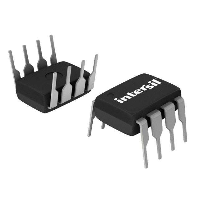
| 描述 | TXRX ESD 5V RS-485/422 8DIP |
| 产品分类 | |
| 品牌 | Intersil |
| 数据手册 | |
| 产品图片 |
|
| 产品型号 | ISL3152EIPZ |
| PCN组件/产地 | |
| rohs | 无铅 / 符合限制有害物质指令(RoHS)规范要求 |
| 产品系列 | - |
| 产品目录页面 | |
| 供应商器件封装 | 8-PDIP |
| 包装 | 管件 |
| 协议 | RS422,RS485 |
| 双工 | 半 |
| 安装类型 | 通孔 |
| 封装/外壳 | 8-DIP(0.300",7.62mm) |
| 工作温度 | -40°C ~ 85°C |
| 接收器滞后 | 20mV |
| 数据速率 | 115Kbps |
| 标准包装 | 50 |
| 电压-电源 | 4.5 V ~ 5.5 V |
| 类型 | 收发器 |
| 驱动器/接收器数 | 1/1 |


- 商务部:美国ITC正式对集成电路等产品启动337调查
- 曝三星4nm工艺存在良率问题 高通将骁龙8 Gen1或转产台积电
- 太阳诱电将投资9.5亿元在常州建新厂生产MLCC 预计2023年完工
- 英特尔发布欧洲新工厂建设计划 深化IDM 2.0 战略
- 台积电先进制程称霸业界 有大客户加持明年业绩稳了
- 达到5530亿美元!SIA预计今年全球半导体销售额将创下新高
- 英特尔拟将自动驾驶子公司Mobileye上市 估值或超500亿美元
- 三星加码芯片和SET,合并消费电子和移动部门,撤换高东真等 CEO
- 三星电子宣布重大人事变动 还合并消费电子和移动部门
- 海关总署:前11个月进口集成电路产品价值2.52万亿元 增长14.8%


PDF Datasheet 数据手册内容提取
DATASHEET ISL3150E, ISL3152E, ISL3153E, ISL3155E, ISL3156E, ISL3158E FN6363 Large 3V Output Swing, 16.5kV ESD, Full Fail-Safe, 1/8 Unit Load, Rev.4.00 RS-485/RS-422 Transceivers Apr 19, 2018 The ISL315xE family of 5V powered RS-485/RS-422 Features transceivers features high output drive and high ESD •High V : 3.1V (Typ) into R = 54Ω OD D protection. The devices withstand ±16.5kV IEC61000-4- 2 ESD strikes without latch-up. The large output voltage •Low bus currents: 125µA constitutes a true 1/8 unit of 3.1V typical into a 54Ω load provides high noise load immunity, and enables the drive of up to 8000ft long bus •Allows for up to 512 transceivers on the bus segments, or eight 120Ω terminations in a star topology. •±16.5kV ESD protection on bus I/O pins These devices possess less than 125µA bus input •High transient overvoltage tolerance of ±100V currents, thus constituting a true 1/8 unit load. The high output drive combined with the low bus input currents •Full fail-safe outputs for open or shorted inputs allows for connecting up to 512 transceivers on the same •Hot plug capability - driver and receiver outputs bus. remain high-impedance during power-up and The receiver inputs feature a full fail-safe design that power-down turns the receiver outputs high when the bus inputs are •Supported data rates: 115kbps, 1Mbps, 20Mbps open or shorted. •Low supply current (driver disabled): 550µA The ISL315xE family includes half and full-duplex transceivers with active-high driver-enable pins and •Ultra-low shutdown current: 70nA active-low receiver enable pins. These transceivers Applications support data rates of 115kbps, 1Mbps, and 20Mbps. •Automated utility e-meter reading systems Their performance is characterized from -40°C to +85°C. •High node count systems Related Literature •PROFIBUS and Fieldbus systems in factory For a full list of related documents, visit our website automation •ISL3150E, ISL3152E, ISL3153E, ISL3155E, •Security camera networks ISL3156E, and ISL3158E product pages •Lighting, elevator, and HVAC control systems in building automation •Industrial process control networks •Networks with star topology •Long-haul networks in coal mines and oil rigs 140 3 130 A) 120 6 x 120Ω ISL3158E m 110 Terms 2 put Current ( 10987600000 8 Txe 1rm20sΩ 2 Txe 1rm20sΩ ut Voltage (V) 10 Out 50 Outp Standard er 40 er -1 Transceiver Driv 3200 1 x 120Ω Driv -2 10 Term 0 20Mbps, 150' UTP, Double 120Ω Termination 0 1 1.5 2 3 4 5 -3 Differential Output Voltage (V) 20ns/Div Figure1.Typical Driver Output Performance of ISL315xE Transceivers FN6363 Rev.4.00 Page 1 of 34 Apr 19, 2018
ISL3150E, ISL3152E, ISL3153E, ISL3155E, ISL3156E, ISL3158E Contents 1. Overview. . . . . . . . . . . . . . . . . . . . . . . . . . . . . . . . . . . . . . . . . . . . . . . . . . . . . . . . . . . . . . . . . . . . . 3 1.1 Typical Operating Circuit . . . . . . . . . . . . . . . . . . . . . . . . . . . . . . . . . . . . . . . . . . . . . . . . . . . . . . 3 1.2 Ordering Information . . . . . . . . . . . . . . . . . . . . . . . . . . . . . . . . . . . . . . . . . . . . . . . . . . . . . . . . . 3 1.3 Pin Configurations. . . . . . . . . . . . . . . . . . . . . . . . . . . . . . . . . . . . . . . . . . . . . . . . . . . . . . . . . . . 5 1.4 Pin Descriptions. . . . . . . . . . . . . . . . . . . . . . . . . . . . . . . . . . . . . . . . . . . . . . . . . . . . . . . . . . . . . 5 2. Specifications. . . . . . . . . . . . . . . . . . . . . . . . . . . . . . . . . . . . . . . . . . . . . . . . . . . . . . . . . . . . . . . . . 6 2.1 Absolute Maximum Ratings. . . . . . . . . . . . . . . . . . . . . . . . . . . . . . . . . . . . . . . . . . . . . . . . . . . . 6 2.2 Thermal Information. . . . . . . . . . . . . . . . . . . . . . . . . . . . . . . . . . . . . . . . . . . . . . . . . . . . . . . . . . 6 2.3 Recommended Operating Conditions . . . . . . . . . . . . . . . . . . . . . . . . . . . . . . . . . . . . . . . . . . . . 6 2.4 Electrical Specifications. . . . . . . . . . . . . . . . . . . . . . . . . . . . . . . . . . . . . . . . . . . . . . . . . . . . . . . 7 3. Test Circuits and Waveforms . . . . . . . . . . . . . . . . . . . . . . . . . . . . . . . . . . . . . . . . . . . . . . . . . . . 11 4. Performance Curves . . . . . . . . . . . . . . . . . . . . . . . . . . . . . . . . . . . . . . . . . . . . . . . . . . . . . . . . . . 14 5. Device Description. . . . . . . . . . . . . . . . . . . . . . . . . . . . . . . . . . . . . . . . . . . . . . . . . . . . . . . . . . . . 17 5.1 Overview . . . . . . . . . . . . . . . . . . . . . . . . . . . . . . . . . . . . . . . . . . . . . . . . . . . . . . . . . . . . . . . . . 17 5.2 Functional Block Diagram . . . . . . . . . . . . . . . . . . . . . . . . . . . . . . . . . . . . . . . . . . . . . . . . . . . . 17 5.3 Operating Modes. . . . . . . . . . . . . . . . . . . . . . . . . . . . . . . . . . . . . . . . . . . . . . . . . . . . . . . . . . . 17 5.4 Device Features. . . . . . . . . . . . . . . . . . . . . . . . . . . . . . . . . . . . . . . . . . . . . . . . . . . . . . . . . . . . 18 6. Application Information. . . . . . . . . . . . . . . . . . . . . . . . . . . . . . . . . . . . . . . . . . . . . . . . . . . . . . . . 21 6.1 Network Design. . . . . . . . . . . . . . . . . . . . . . . . . . . . . . . . . . . . . . . . . . . . . . . . . . . . . . . . . . . . 21 6.2 Transient Protection. . . . . . . . . . . . . . . . . . . . . . . . . . . . . . . . . . . . . . . . . . . . . . . . . . . . . . . . . 26 6.3 Layout Guidelines . . . . . . . . . . . . . . . . . . . . . . . . . . . . . . . . . . . . . . . . . . . . . . . . . . . . . . . . . . 26 7. Revision History. . . . . . . . . . . . . . . . . . . . . . . . . . . . . . . . . . . . . . . . . . . . . . . . . . . . . . . . . . . . . . 28 8. Package Outline Drawings . . . . . . . . . . . . . . . . . . . . . . . . . . . . . . . . . . . . . . . . . . . . . . . . . . . . . 29 FN6363 Rev.4.00 Page 2 of 34 Apr 19, 2018
ISL3150E, ISL3152E, ISL3153E, ISL3155E, ISL3156E, ISL3158E 1. Overview 1. Overview 1.1 Typical Operating Circuit 5V 5V 100n 100n 8 8 RB 10k VCC 10k VCC (optional) RB A RO R A/Y (optional) RO R B RT RE RE RMLC7U8 DE RT RMLC7U8 DE (optRioBn al) B/Z Y DI DI D D Z 10k 10k GND RB 10k 10k GND (optional) 5 5 Figure2.Typical Operating Circuits of Half-Duplex and Full-Duplex Transceivers 1.2 Ordering Information Tape and Reel Package Part Number (Notes2, 3) Part Marking Temp. Range (°C) (Units) (Note1) (RoHS Compliant) Pkg. Dwg. # ISL3150EIBZ 3150EIBZ -40 to +85 - 14 Ld SOIC M14.15 ISL3150EIBZ-T 3150EIBZ -40 to +85 2.5k 14 Ld SOIC M14.15 ISL3150EIBZ-T7A 3150EIBZ -40 to +85 250 14 Ld SOIC M14.15 ISL3150EIUZ 3150Z -40 to +85 - 10 Ld MSOP M10.118 ISL3150EIUZ-T 3150Z -40 to +85 2.5k 10 Ld MSOP M10.118 ISL3150EIUZ-T7A 3150Z -40 to +85 250 10 Ld MSOP M10.118 ISL3152EIBZ 3152EIBZ -40 to +85 - 8 Ld SOIC M8.15 ISL3152EIBZ-T 3152EIBZ -40 to +85 2.5k 8 Ld SOIC M8.15 ISL3152EIBZ-T7 3152EIBZ -40 to +85 1k 8 Ld SOIC M8.15 ISL3152EIBZ-T7A 3152EIBZ -40 to +85 250 8 Ld SOIC M8.15 ISL3152EIPZ ISL3152 EIPZ -40 to +85 - 8 Ld PDIP E8.3 ISL3152EIUZ 3152Z -40 to +85 - 8 Ld MSOP M8.118 ISL3152EIUZ-T 3152Z -40 to +85 2.5k 8 Ld MSOP M8.118 ISL3152EIUZ-T7A 3152Z -40 to +85 250 8 Ld MSOP M8.118 ISL3153EIBZ-T 3153EIBZ -40 to +85 2.5k 14 Ld SOIC M14.15 ISL3153EIUZ 3153Z -40 to +85 - 10 Ld MSOP M10.118 ISL3153EIUZ-T 3153Z -40 to +85 2.5k 10 Ld MSOP M10.118 ISL3153EIUZ-T7A 3153Z -40 to +85 250 10 Ld MSOP M10.118 ISL3155EIBZ 3155EIBZ -40 to +85 - 8 Ld SOIC M8.15 ISL3155EIBZ-T 3155EIBZ -40 to +85 2.5k 8 Ld SOIC M8.15 ISL3155EIBZ-T7A 3155EIBZ -40 to +85 250 8 Ld SOIC M8.15 ISL3155EIUZ 3155Z -40 to +85 - 8 Ld MSOP M8.118 ISL3155EIUZ-T 3155Z -40 to +85 2.5k 8 Ld MSOP M8.118 ISL3156EIBZ 3156EIBZ -40 to +85 - 14 Ld SOIC M14.15 FN6363 Rev.4.00 Page 3 of 34 Apr 19, 2018
ISL3150E, ISL3152E, ISL3153E, ISL3155E, ISL3156E, ISL3158E 1. Overview Tape and Reel Package Part Number (Notes2, 3) Part Marking Temp. Range (°C) (Units) (Note1) (RoHS Compliant) Pkg. Dwg. # ISL3156EIBZ-T 3156EIBZ -40 to +85 2.5k 14 Ld SOIC M14.15 ISL3156EIBZ-T7A 3156EIBZ -40 to +85 250 14 Ld SOIC M14.15 ISL3156EIUZ 3156Z -40 to +85 - 10 Ld MSOP M10.118 ISL3156EIUZ-T 3156Z -40 to +85 2.5k 10 Ld MSOP M10.118 ISL3156EIUZ-T7A 3156Z -40 to +85 250 10 Ld MSOP M10.118 ISL3158EIBZ 3158EIBZ -40 to +85 - 8 Ld SOIC M8.15 ISL3158EIBZ-T 3158EIBZ -40 to +85 2.5k 8 Ld SOIC M8.15 ISL3158EIBZ-T7A 3158EIBZ -40 to +85 250 8 Ld SOIC M8.15 ISL3158EIUZ 3158Z -40 to +85 - 8 Ld MSOP M8.118 ISL3158EIUZ-T 3158Z -40 to +85 2.5k 8 Ld MSOP M8.118 ISL3158EIUZ-T7A 3158Z -40 to +85 250 8 Ld MSOP M8.118 Notes: 1. Refer to TB347 for details about reel specifications. 2. These Pb-free plastic packaged products employ special Pb-free material sets, molding compounds/die attach materials, and 100% matte tin plate plus anneal (e3 termination finish, which is RoHS compliant and compatible with both SnPb and Pb-free soldering operations). Pb-free products are MSL classified at Pb-free peak reflow temperatures that meet or exceed the Pb-free requirements of IPC/JEDEC J STD-020. 3. For Moisture Sensitivity Level (MSL), see the product information pages for the ISL3150E, ISL3152E, ISL3153E, ISL3155E, ISL3156E, and ISL3158E. For more information about MSL, see TB363. Table1.Key Differences of Device Features Part Number Duplex Data Rate (Mbps) Rise/Fall Time (ns) Tx/Rx Skew (ns) Bus ESD (kV) Pin Count ISL3150E Full 0.115 1100 12/4 ±10 10, 14 ISL3152E Half 0.115 1100 12/4 ±16 8 ISL3153E Full 1 150 3/4 ±10 10, 14 ISL3155E Half 1 150 3/4 ±16 8 ISL3156E Full 20 8 0.2/2.5 ±10 10, 14 ISL3158E Half 20 8 0.2/2.5 ±16 8 FN6363 Rev.4.00 Page 4 of 34 Apr 19, 2018
ISL3150E, ISL3152E, ISL3153E, ISL3155E, ISL3156E, ISL3158E 1. Overview 1.3 Pin Configurations ISL3152E, ISL3155E, ISL3158E ISL3150E, ISL3153E, ISL3156E ISL3150E, ISL3153E, ISL3156E (8 Ld MSOP, 8 Ld SOIC, 8 Ld PDIP) (10 Ld MSOP) (14 Ld SOIC) Top View Top View Top View RO 1 R 8 VCC RO 1 R 10 VCC NC 1 14 VCC RE 2 7 B/Z RE 2 9 A RO 2 R 13 NC DE 3 6 A/Y DE 3 8 B RE 3 12 A DI 4 D 5 GND DI 4 D 7 Z DE 4 11 B GND 5 6 Y DI 5 D 10 Z GND 6 9 Y GND 7 8 NC 1.4 Pin Descriptions 8 Ld 10 Ld 14 Ld Pin SOIC MSOP SOIC Name Function 1 1 2 RO Receiver output: If A-B ≥ -50mV, RO is high; If A-B ≤ -200mV, RO is low. RO is Fail-safe High if A and B are unconnected (open) or shorted. 2 2 3 RE Receiver output enable. RO is enabled when RE is low; RO is high impedance when RE is high. 3 3 4 DE Driver output enable. The driver outputs, Y and Z, are enabled by bringing DE high. They are high impedance when DE is low. 4 4 5 DI Driver input. A low on DI forces output Y low and output Z high. Similarly, a high on DI forces output Y high and output Z low. 5 5 6, 7 GND Ground connection. 6 – – A/Y Non-inverting receiver input and non-inverting driver output. Pin is an input if DE = 0; pin is an output if DE = 1. 7 – – B/Z Inverting receiver input and inverting driver output. Pin is an input if DE = 0; pin is an output if DE = 1. – 6 9 Y Non-inverting driver output. – 7 10 Z Inverting driver output. – 8 11 B Inverting receiver input. – 9 12 A Non-inverting receiver input. 8 10 – V System power supply input (4.5V to 5.5V). CC – – 1, 8, 13 NC No connection. FN6363 Rev.4.00 Page 5 of 34 Apr 19, 2018
ISL3150E, ISL3152E, ISL3153E, ISL3155E, ISL3156E, ISL3158E 2. Specifications 2. Specifications 2.1 Absolute Maximum Ratings Parameter (Note4) Minimum Maximum Unit V to Ground 7 V CC Input Voltages at DI, DE, RE -0.3 V + 0.3 V CC Bus I/O Voltages at A/Y, B/Z, A, B, Y, Z -9 13 V Transient Pulse Voltages through 100Ω at A/Y, B/Z, A, B, Y, Z (Note5) ±100 V RO -0.3 V + 0.3 V CC Short Circuit Duration at Y, Z Continuous ESD Rating See “Electrical Specifications” on page8. Note: 4. Absolute Maximum ratings mean the device will not be damaged if operated under these conditions. It does not guarantee performance. 5. Tested according to TIA/EIA-485-A, Section 4.2.6 (±100V for 15µs at a 1% duty cycle). CAUTION: Do not operate at or near the maximum ratings listed for extended periods of time. Exposure to such conditions may adversely impact product reliability and result in failures not covered by warranty. 2.2 Thermal Information Thermal Resistance (Typical, Note6) θ (°C/W) JA 8 Ld SOIC 105 8 Ld MSOP, PDIP 140 10 Ld MSOP 130 14 Ld SOIC 130 Notes: 6. θ is measured with the component mounted on a high-effective thermal conductivity test board in free air. See TB379 for JA details. Parameter Minimum Maximum Unit Maximum Junction Temperature (Plastic Package) +150 °C Maximum Storage Temperature Range -65 +150 °C Pb-Free Reflow Profile (Note7) See TB493 Note: 7. Pb-free PDIPs can be used for through-hole wave solder processing only. They are not intended for use in Reflow solder processing applications. 2.3 Recommended Operating Conditions Parameter Minimum Maximum Unit Supply Voltage 4.5 5.5 V Temperature Range -40 +85 °C Bus Pin Common-Mode Voltage Range -7 +12 V FN6363 Rev.4.00 Page 6 of 34 Apr 19, 2018
ISL3150E, ISL3152E, ISL3153E, ISL3155E, ISL3156E, ISL3158E 2. Specifications 2.4 Electrical Specifications Test Conditions: V = 4.5V to 5.5V; unless otherwise specified. Typical values are at V = 5V, T = +25°C (Note8). Boldface limits CC CC A apply across the operating temperature range, -40°C to +85°C. Temp Min Parameter Symbol Test Conditions (°C) (Note16) Typ Max (Note16) Unit DC Characteristics Driver Differential Output V Full - - V V OD1 CC Voltage (Noload) Driver Differential Output V R = 100Ω (RS-422) (Figure3) Full 2.8 3.6 - V OD2 L Voltage (Loaded) R = 54Ω (RS-485) (Figure3) Full 2.4 3.1 V V L CC R = 15Ω (Eight 120Ω terminations) +25 - 1.65 - V L (Note17) R = 60Ω, -7V ≤ V ≤ 12V (Figure4) Full 2.4 3 - V L CM Change in Magnitude of ΔV R = 54Ω or 100Ω (Figure3) Full - 0.01 0.2 V OD L Driver Differential Output Voltage Driver Common-Mode Output V R = 54Ω or 100Ω (Figure3) Full - - 3.15 V OC L Voltage Change in Magnitude of ΔV R = 54Ω or 100Ω (Figure3) Full - 0.01 0.2 V OC L Driver Common-Mode Output Voltage Logic Input High Voltage V DE, DI, RE Full 2 - - V IH Logic Input Low Voltage V DE, DI, RE Full - - 0.8 V IL DI Input Hysteresis Voltage V +25 - 100 - mV HYS Logic Input Current I DE, DI, RE Full -2 - 2 µA IN1 Input Current (A, B, A/Y, B/Z) I DE = 0V, V = 0V V = 12V Full - 70 125 µA IN2 CC IN or 5.5V V = -7V Full -75 55 - µA IN Output Leakage Current I RE = 0V, DE = 0V, V = 12V Full - 1 40 µA IN3 IN (Y,Z) (FullDuplex Versions V =0V or 5.5V CC V = -7V Full -40 -9 - µA Only) IN Output Leakage Current I RE = V , DE = 0V, V = 12V Full - 1 20 µA IN4 CC IN (Y,Z) in Shutdown Mode (Full V = 0V or 5.5V CC V = -7V Full -20 -9 - µA Duplex) IN Driver Short-Circuit Current, I DE = V , -7V ≤ V or V ≤ 12V Full - - ±250 mA OSD1 CC Y Z V = High or Low (Note10) O Receiver Differential V -7V ≤ V ≤ 12V Full -200 -90 -50 mV TH CM Threshold Voltage Receiver Input Hysteresis ΔV V = 0V +25 - 20 - mV TH CM Receiver Output High Voltage V I = -8mA, V = -50mV Full V - 1.2 4.3 - V OH O ID CC Receiver Output Low Voltage V I = -8mA, V = -200mV Full - 0.25 0.4 V OL O ID Receiver Output Low Current I V = 1V, V = -200mV Full 20 28 - mA OL O ID Three-State (High I 0.4V ≤ V ≤ 2.4V Full -1 0.03 1 µA OZR O Impedance) Receiver Output Current Receiver Input Resistance R -7V ≤ V ≤ 12V Full 96 160 - kΩ IN CM FN6363 Rev.4.00 Page 7 of 34 Apr 19, 2018
ISL3150E, ISL3152E, ISL3153E, ISL3155E, ISL3156E, ISL3158E 2. Specifications Test Conditions: V = 4.5V to 5.5V; unless otherwise specified. Typical values are at V = 5V, T = +25°C (Note8). Boldface limits CC CC A apply across the operating temperature range, -40°C to +85°C. (Continued) Temp Min Parameter Symbol Test Conditions (°C) (Note16) Typ Max (Note16) Unit Receiver Short-Circuit I 0V ≤ V ≤ V Full ±7 65 ±85 mA OSR O CC Current Supply Current No-Load Supply Current I Half duplex versions, DE = V , RE=X, Full - 650 800 µA CC CC (Note9) DI = 0V or V CC All versions, DE = 0V, RE = 0V, or full Full - 550 700 µA duplex versions, DE = V , RE = X. CC DI=0V or V CC Shutdown Supply Current I DE = 0V, RE = V , DI = 0V or V Full - 0.07 3 µA SHDN CC CC ESD Performance RS-485 Pins (A, Y, B, Z, A/Y, IEC61000-4-2, Half duplex +25 - ±16.5 - kV B/Z) Air-Gap Discharge Full duplex +25 - ±10 - kV Method IEC61000-4-2, Contact Discharge +25 - ±9 - kV Method Human Body Model, from bus pins to +25 - ±16.5 - kV GND All Pins Human Body Model, per MIL-STD-883 +25 - ±7 - kV Method 3015 Machine Model +25 - 400 - V Driver Switching Characteristics (115kbps Versions; ISL3150E, ISL3152E) Driver Differential Output t t R = 54Ω, C = 100pF (Figure5) Full 500 970 1300 ns PLH, PHL DIFF L Delay Driver Differential Output t R = 54Ω, C = 100pF (Figure5) Full - 12 50 ns SKEW DIFF L Skew Driver Differential Rise or t , t R = 54Ω, C = 100pF (Figure5) Full 700 1100 1600 ns R F DIFF L FallTime Maximum Data Rate f C = 820pF (Figure7, Note18) Full 115 2000 - kbps MAX D Driver Enable to Output High t R = 500Ω, C = 100pF, SW = GND Full - 300 600 ns ZH L L (Figure6, Note11) Driver Enable to Output Low t R = 500Ω, C = 100pF, SW = V Full - 130 500 ns ZL L L CC (Figure6, Note11) Driver Disable from Output t R = 500Ω, C = 15pF, SW = V Full - 50 65 ns LZ L L CC Low (Figure6) Driver Disable from Output t R = 500Ω, C = 15pF, Full - 35 60 ns HZ L L High SW = GND (Figure6) Time to Shutdown t (Note13) Full 60 160 600 ns SHDN Driver Enable from Shutdown t R = 500Ω, C = 100pF, SW = GND Full - - 250 ns ZH(SHDN) L L to Output High (Figure6, Notes13, 14) Driver Enable from Shutdown t R = 500Ω, C = 100pF, SW = V Full - - 250 ns ZL(SHDN) L L CC to Output Low (Figure6, Notes13, 14) Driver Switching Characteristics (1Mbps Versions; ISL3153E, ISL3155E) Driver Differential Output t t R = 54Ω, C = 100pF (Figure5) Full 150 270 400 ns PLH, PHL DIFF L Delay FN6363 Rev.4.00 Page 8 of 34 Apr 19, 2018
ISL3150E, ISL3152E, ISL3153E, ISL3155E, ISL3156E, ISL3158E 2. Specifications Test Conditions: V = 4.5V to 5.5V; unless otherwise specified. Typical values are at V = 5V, T = +25°C (Note8). Boldface limits CC CC A apply across the operating temperature range, -40°C to +85°C. (Continued) Temp Min Parameter Symbol Test Conditions (°C) (Note16) Typ Max (Note16) Unit Driver Differential Output t R = 54Ω, C = 100pF (Figure5) Full - 3 10 ns SKEW DIFF L Skew Driver Differential Rise or t , t R = 54Ω, C = 100pF (Figure5) Full 150 325 450 ns R F DIFF L FallTime Maximum Data Rate f C = 820pF (Figure7, Note18) Full 1 8 - Mbps MAX D Driver Enable to Output High t R = 500Ω, C = 100pF, SW = GND Full - 110 200 ns ZH L L (Figure6, Note11) Driver Enable to Output Low t R = 500Ω, C = 100pF, SW = V Full - 60 200 ns ZL L L CC (Figure6, Note11) Driver Disable from Output t R = 500Ω, C = 15pF, SW = V Full - 50 65 ns LZ L L CC Low (Figure6) Driver Disable from Output t R = 500Ω, C = 15pF, SW = GND Full - 35 60 ns HZ L L High (Figure6) Time to Shutdown t (Note13) Full 60 160 600 ns SHDN Driver Enable from Shutdown t R = 500Ω, C = 100pF, SW = GND Full - - 250 ns ZH(SHDN) L L to Output High (Figure6, Notes13, 14) Driver Enable from Shutdown t R = 500Ω, C = 100pF, SW = V Full - - 250 ns ZL(SHDN) L L CC to Output Low (Figure6, Notes13, 14) Driver Switching Characteristics (20Mbps Versions; ISL3156E, ISL3158E) Driver Differential Output t t R = 54Ω, C = 100pF (Figure5) Full - 21 30 ns PLH, PHL DIFF L Delay Driver Differential Output t R = 54Ω, C = 100pF (Figure5) Full - 0.2 3 ns SKEW DIFF L Skew Driver Differential Rise or Fall t , t R = 54Ω, C = 100pF (Figure5) Full - 12 16 ns R F DIFF L Time Maximum Data Rate f C = 470pF (Figure7, Note18) Full 20 55 - Mbps MAX D Driver Enable to Output High t R = 500Ω, C = 100pF, SW = GND Full - 30 45 ns ZH L L (Figure6, Note11) Driver Enable to Output Low t R = 500Ω, C = 100pF, SW = V Full - 28 45 ns ZL L L CC (Figure6, Note11) Driver Disable from Output t R = 500Ω, C = 15pF, SW = V Full - 50 65 ns LZ L L CC Low (Figure6) Driver Disable from Output t R = 500Ω, C = 15pF, SW = GND Full - 38 60 ns HZ L L High (Figure6) Time to Shutdown t (Note13) Full 60 160 600 ns SHDN Driver Enable from Shutdown t R = 500Ω, C = 100pF, SW = GND Full - - 200 ns ZH(SHDN) L L to Output High (Figure6, Notes13, 14) Driver Enable from Shutdown t R = 500Ω, C = 100pF, SW = V Full - - 200 ns ZL(SHDN) L L CC to Output Low (Figure6, Notes13, 14) Receiver Switching Characteristics (115kbps and 1Mbps Versions; ISL3150E through ISL3155E) Maximum Data Rate f (Figure8, Note18) Full 1 12 - Mbps MAX Receiver Input to Output t , (Figure8) Full - 100 150 ns PLH Delay t PHL Receiver Skew | t - t | t (Figure8) Full - 4 10 ns PLH PHL SKD FN6363 Rev.4.00 Page 9 of 34 Apr 19, 2018
ISL3150E, ISL3152E, ISL3153E, ISL3155E, ISL3156E, ISL3158E 2. Specifications Test Conditions: V = 4.5V to 5.5V; unless otherwise specified. Typical values are at V = 5V, T = +25°C (Note8). Boldface limits CC CC A apply across the operating temperature range, -40°C to +85°C. (Continued) Temp Min Parameter Symbol Test Conditions (°C) (Note16) Typ Max (Note16) Unit Receiver Enable to Output t R = 1kΩ, C = 15pF, SW = V Full - 9 20 ns ZL L L CC Low (Figure9, Note12) Receiver Enable to Output t R = 1kΩ, C = 15pF, SW = GND Full - 7 20 ns ZH L L High (Figure9, Note12) Receiver Disable from Output t R = 1kΩ, C = 15pF, SW = V Full - 8 15 ns LZ L L CC Low (Figure9) Receiver Disable from Output t R = 1kΩ, C = 15pF, SW = GND Full - 8 15 ns HZ L L High (Figure9) Time to Shutdown t (Note13) Full 60 160 600 ns SHDN Receiver Enable from t R = 1kΩ, C = 15pF, SW = GND Full - - 200 ns ZH(SHDN) L L Shutdown to Output High (Figure9, Notes13, 15) Receiver Enable from t R = 1kΩ, C = 15pF, SW = V Full - - 200 ns ZL(SHDN) L L CC Shutdown to Output Low (Figure9, Notes13, 15) Receiver Switching Characteristics (20Mbps Versions; ISL3156E, ISL3158E) Maximum Data Rate f (Figure8, Note18) Full 20 30 - Mbps MAX Receiver Input to Output t , (Figure8) Full - 33 45 ns PLH Delay t PHL Receiver Skew | t - t | t (Figure8) Full - 2.5 5 ns PLH PHL SKD Receiver Enable to Output t R = 1kΩ, C = 15pF, SW = V Full - 8 15 ns ZL L L CC Low (Figure9, Note12) Receiver Enable to Output t R = 1kΩ, C = 15pF, SW = GND Full - 7 15 ns ZH L L High (Figure9, Note12) Receiver Disable from Output t R = 1kΩ, C = 15pF, SW = V Full - 8 15 ns LZ L L CC Low (Figure9) Receiver Disable from Output t R = 1kΩ, C = 15pF, SW = GND Full - 8 15 ns HZ L L High (Figure9) Time to Shutdown t (Note13) Full 60 160 600 ns SHDN Receiver Enable from t R = 1kΩ, C = 15pF, SW = GND Full - - 200 ns ZH(SHDN) L L Shutdown to Output High (Figure9), (Notes13, 15) Receiver Enable from t R = 1kΩ, C = 15pF, SW = V Full - - 200 ns ZL(SHDN) L L CC Shutdown to Output Low (Figure9), (Notes13, 15) Notes: 8. All currents in to device pins are positive; all currents out of device pins are negative. All voltages are referenced to device ground unless otherwise specified. 9. Supply current specification is valid for loaded drivers when DE = 0V. 10. Applies to peak current. See “Performance Curves” beginning on page14 for more information. 11. Keep RE = 0 to prevent the device from entering SHDN. 12. The RE signal high time must be short enough (typically <100ns) to prevent the device from entering SHDN. 13. Transceivers are put into shutdown by bringing RE high and DE low. If the inputs are in this state for less than 60ns, the parts are guaranteed not to enter shutdown. If the inputs are in this state for at least 600ns, the parts are guaranteed to have entered shutdown. See “Low Current Shutdown Mode” on page20. 14. Keep RE = V , and set the DE signal low time >600ns to ensure that the device enters SHDN. CC 15. Set the RE signal high time >600ns to ensure that the device enters SHDN. 16. Parameters with MIN and/or MAX limits are 100% tested at +25°C, unless otherwise specified. Temperature limits established by characterization and are not production tested. 17. See Figure11 on page14 for more information and for performance over temperature. 18. Limits established by characterization and are not production tested. FN6363 Rev.4.00 Page 10 of 34 Apr 19, 2018
ISL3150E, ISL3152E, ISL3153E, ISL3155E, ISL3156E, ISL3158E 3. Test Circuits and Waveforms 3. Test Circuits and Waveforms VCC DE Y RL/2 Y VOH DI 0V or 3V D VOD Z VOL Z RL/2 VOC VOC VOC Figure3.Measurement of Driver Differential Output Voltage with Differential Load VCC 375 DE Y DI 0V or 3V D VOD RL = 60 Z VCM -7V to +12V 375 Figure4.Measurement of Driver Differential Output Voltage with Common-Mode Load 3V DI 50% 50% 1.5V VCC CL = 100pF 0V tPLH tPHL DE Y DI Z VOH D VOD RDIFF Z CL = 100pF Y VOL Skew = |tPLH - tPHL| 90% 90% +VOD VOD (Y - Z) 10% 10% -VOD tR tF Figure5.Measurement of Driver Propagation Delay and Differential Transition Times FN6363 Rev.4.00 Page 11 of 34 Apr 19, 2018
ISL3150E, ISL3152E, ISL3153E, ISL3155E, ISL3156E, ISL3158E 3. Test Circuits and Waveforms VCC Y 500 DI D SW 3V DE Z CL DE 1.5V 1.5V 0V tZH(SHDN) tZH tHZ VOH VOH - 0.5V CL Y, Z 2.3V Parameter Output RE DI SW (pF) 0V t Y/Z X 1/0 GND 15 HZ tZL(SHDN) tZL tLZ t Y/Z X 0/1 V 15 LZ CC VCC t Y/Z 0 (Note11) 1/0 GND 100 ZH Y, Z 2.3V tZL Y/Z 0 (Note11) 0/1 VCC 100 VOL VOL + 0.5V t Y/Z 1 (Note14) 1/0 GND 100 ZH(SHDN) t Y/Z 1 (Note14) 0/1 V 100 ZL(SHDN) CC Figure6.Measurement of Driver Enable and Disable Times VCC 3V DI DE Y DI 0V D VOD 60 CD Z +VOD Y, Z 0V -VOD Figure7.Measurement of Driver Data Rate +1.5V A A 0V 0V RO -1.5V R B 15pF tPLH tPHL RE VCC RO 1.5V 1.5V 0V Figure8.Measurement of Receiver Propagation Delay and Data Rate FN6363 Rev.4.00 Page 12 of 34 Apr 19, 2018
ISL3150E, ISL3152E, ISL3153E, ISL3155E, ISL3156E, ISL3158E 3. Test Circuits and Waveforms VCC A 1k RO 3V R SW B RE 15pF 1.5V 1.5V RE 0V tZH(SHDN) tZH tHZ VOH VOH - 0.5V RO 1.5V Parameter DE A SW 0V t 0 +1.5V GND HZ tZL(SHDN) tZL tLZ t 0 -1.5V V LZ CC tZH (Note12) 0 +1.5V GND VCC t (Note12) 0 -1.5V V RO 1.5V t ZL (Note15) 0 +1.5V GNCCD VOL VOL + 0.5V ZH(SHDN) t (Note15) 0 -1.5V V ZL(SHDN) CC Figure9.Measurement of Receiver Enable and Disable Times FN6363 Rev.4.00 Page 13 of 34 Apr 19, 2018
ISL3150E, ISL3152E, ISL3153E, ISL3155E, ISL3156E, ISL3158E 4. Performance Curves 4. Performance Curves V = 5V, T = +25°C; Unless otherwise specified CC A V) 5.0 V) 5.0 (D (D O 4.5 O 4.5 54Ω – V 4.0 VOH – V 4.0 e e g 3.5 g 3.5 a a olt 3.0 olt 3.0 V V Output 22..50 VOL Output 22..50 TA = +85oC TA = 25oC 15Ω al 1.5 al 1.5 nti 1.0 nti 1.0 e e r 0.5 r 0.5 e e Diff 00 20 40 60 80 100 120 140 Diff 00 20 40 60 80 100 120 140 Driver Output Current – IO (mA) Driver Output Current – IO (mA) Figure10.Driver Output High and Low Voltages vs Figure11.Driver Differential Output Voltage vs Output Output Current Current V (V)B 54..05 FFiiggu. r4e T4e Tset sCt iCrciurcituit VA V (V)OD 33..76 , A 4.0 – RDIFF = 100Ω ge – V 33..50 VOD oltage 33..54 ut Volta 22..50 VOC utput V 33..32 p 1.5 O r Out 1.0 VB ntial 3.1 RDIFF = 54Ω ve 0.5 re 3.0 Dri 0-8 -6 -4 -2 0 2 4 6 8 10 12 Diffe 2.9-40 -20 0 20 40 60 80 100 Common-Mode Voltage – VCM (V) Temperature (oC) Figure12.Driver Output Voltages vs Common-Mode Figure13.Driver Differential Output Voltage vs Voltage Temperature V) 3.5 70 (D D, DE = VCC A) – VO 3.0 RRDD= = 5 544ΩΩ (mO 60 VOL,+ 25oC Voltage 22..50 urrent – I 5400 VOL,+ 85oC utput 1.5 put C 30 VOH,+ 25oC rential O 10..05 river Out 2100 VOH,+ 85oC e D Diff 00 1 2 3 4 5 00 1 2 3 4 5 Supply Voltage – VCC (V) Supply Voltage – VCC (V) Figure14.Driver Output Voltage vs Supply Voltage Figure15.Receiver Output Voltage vs Output Current FN6363 Rev.4.00 Page 14 of 34 Apr 19, 2018
ISL3150E, ISL3152E, ISL3153E, ISL3155E, ISL3156E, ISL3158E 4. Performance Curves V = 5V, T = +25°C; Unless otherwise specified (Continued) CC A 70 A) RL = 54Ω, CL = 100pF (mO 60 O (V) DI nt – I 50 ata I/ RO rre 40 DE, RE = VCC D 5V/Div Cu RD = 54Ω ut 30 CL = 100pF p r Out 20 O (V) B/Z Drive 10 us I/ 1V/Div 0 B A/Y 0 10 20 30 40 50 60 70 80 90 100110120 Data Rate (kbps) Time: 1μs/Div Figure16.Supply Current vs Data Rate Figure17.Waveforms (ISL3150E, ISL3152E) (ISL3150E,ISL3152E) 70 A) RL = 54Ω, CL = 100pF (mO 60 O (V) DI urrent – I 5400 DRED ,= R 5E4 Ω= VCC Data I/ RO 5V/Div C ut 30 CL = 100pF p r Out 20 O (V) B/Z Drive 10 us I/ 1V/Div 0 B A/Y 0 0.1 0.2 0.3 0.4 0.5 0.6 0.7 0.8 0.9 1.0 Data Rate (Mbps) Time: 400ns/Div Figure18.Supply Current vs Data Rate Figure19.Waveforms (ISL3153E, ISL3155E) (ISL3153E,ISL3155E) 100 (mA)O 9800 O (V) DI RL = 54Ω, CL = 100pF – I 70 a I/ nt at RO e 60 D 5V/Div Curr 50 DE, RE = VCC ut 40 RD = 54Ω utp 30 CL = 100pF V) r O 20 O ( B/Z Drive 100 Bus I/ A/Y 1V/Div 0 2 4 6 8 10 12 14 16 18 20 Time: 20ns/Div Data Rate (Mbps) Figure20.Supply Current vs Data Rate Figure21.Waveforms (ISL3156E, ISL3158E) (ISL3156E,ISL3158E) FN6363 Rev.4.00 Page 15 of 34 Apr 19, 2018
ISL3150E, ISL3152E, ISL3153E, ISL3155E, ISL3156E, ISL3158E 4. Performance Curves V = 5V, T = +25°C; Unless otherwise specified (Continued) CC A 1010 12 1005 11 s) 1000 y (n 995 10 a el 990 s) 9 D n gation 998850 tPLH Skew ( 87 a 975 p o tPHL 6 r 970 P 965 5 960 4 -40 -20 0 20 40 60 80 100 -40 -20 0 20 40 60 80 100 Temperature (oC) Temperature (oC) Figure22.Differential Rise/Fall Times vs Temperature Figure23.Differential Propagation Delay vs (ISL3150E, ISL3152E) Temperature (ISL3150E, ISL3152E) 290 3.25 288 3.00 s) 286 n 2.75 y ( 284 a el 282 s) 2.50 n D 280 tPLH w (n 2.25 gatio 278 tPHL Ske 2.00 a 276 op 1.75 r 274 P 1.50 272 270 1.25 -40 -20 0 20 40 60 80 100 -40 -20 0 20 40 60 80 100 Temperature (oC) Temperature (oC) Figure24.Differential Rise/Fall Times vs Temperature Figure25.Differential Propagation Delay vs (ISL3153E, ISL3155E) Temperature (ISL3153E, ISL3155E) 23.0 0.26 22.5 0.24 s) 22.0 y (n 21.5 tPLH 0.22 n Dela 2210..05 tPHL w (ns) 00..2108 o e ati 20.0 Sk 0.16 g a 19.5 p 0.14 o r 19.0 P 0.12 18.5 18.0 0.10 -40 -20 0 20 40 60 80 100 -40 -20 0 20 40 60 80 100 Temperature (oC) Temperature (oC) Figure26.Differential Rise/Fall Times vs Temperature Figure27.Differential Propagation Delay vs (ISL3156E, ISL3158E) Temperature (ISL3156E, ISL3158E) FN6363 Rev.4.00 Page 16 of 34 Apr 19, 2018
ISL3150E, ISL3152E, ISL3153E, ISL3155E, ISL3156E, ISL3158E 5. Device Description 5. Device Description 5.1 Overview The ISL3150E, ISL3153E, and ISL3156E are full-duplex RS-485 transceivers, and the ISL3152E, ISL3155E, and ISL3158E are half-duplex RS-485 transceivers. All transceivers feature a large output signal swing that is 60% higher than standard compliant transceivers. The devices are available in three speed grades suitable for data transmission up to 115kbps, 1Mbps, and 20Mbps. Each transceiver has an active-high driver enable and an active-low receiver enable function. A shutdown current as low as 70nA can be accomplished by disabling both the driver and receiver for more than 600ns. 5.2 Functional Block Diagram VCC VCC A RO R RO R B RE B/Z RE DE A/Y DE Y DI D DI D Z GND GND Figure28.Block Diagram Figure29.Block Diagram ISL3150E, ISL3153E, ISL3156E ISL3152E, ISL3155E, ISL3158E 5.3 Operating Modes 5.3.1 Driver Operation A logic high at the driver enable pin, DE, activates the driver and causes the differential driver outputs, Y and Z, to follow the logic states at the data input, DI. A logic high at DI causes Y to turn high and Z to turn low. In this case, the differential output voltage, defined as V = V – V , is positive. A logic low at DI reverses the output states reverse, turning Y low and Z high, OD Y Z thus making V negative. OD A logic low at DE disables the driver, making Y and Z high-impedance. In this condition the logic state at DI is irrelevant. To ensure the driver remains disabled after device power-up, it is recommended to connect DE through a 1kΩ to 10kΩ pull-down resistor to ground. Table2.Driver Truth Table Inputs Outputs RE DE DI Y Z Function X H H H L Actively drives bus high X H L L H Actively drives bus low L L X Z Z Driver disabled, outputs high-impedance H L X Z* Z* Shutdown mode: driver and receiver disabled for more than 600ns Note:* See Shutdown mode explanation in “Low Current Shutdown Mode” on page20. FN6363 Rev.4.00 Page 17 of 34 Apr 19, 2018
ISL3150E, ISL3152E, ISL3153E, ISL3155E, ISL3156E, ISL3158E 5. Device Description 5.3.2 Receiver Operation A logic low at the receiver enable pin, RE, activates the receiver and causes its output, RO, to follow the bus voltage at the differential receiver inputs, A and B. Here, the bus voltage is defined as V = V - V . AB A B For V ≥ -0.05V, RO turns high, and for V ≤ -0.2V, RO turns low. For input voltages between -50mV and AB AB -200mV, the state of RO is undetermined, and thus could be high or low. A logic high at RE disables the receiver, making RO high-impedance. In this condition the polarity and magnitude of the input voltage is irrelevant. To ensure the receiver output remains high when the receiver is disabled, it is recommended to connect RO, using a 1kΩ to 10kΩ pull-up resistor to V . CC To enable the receiver to immediately monitor the bus traffic after device power-up, connect RE through a 1kΩ to 10kΩ pull-down resistor to ground. Table3.Receiver Truth Table Inputs Outputs RE DE A – B RO Function L X V ≥ -0.05V H RO is data-driven high AB L X -0.05V > V > -0.2V Undetermined Actively drives bus low AB L X V ≤ -0.2V L RO is data-driven low AB L X Inputs Open/Shorted H RO is failsafe-high H H X Z Receiver disabled, RO is high-impedance H L X Z* Shutdown mode: driver and receiver disabled for more than 600ns Note:* See Shutdown mode explanation in “Low Current Shutdown Mode” on page20. 5.4 Device Features 5.4.1 Large Output Signal Swing The ISL315xE family has a 60% larger differential output voltage swing than standard RS-485 transceivers. It delivers a minimum V of 2.4V across a 54Ω differential load, or 1.65V across a 15Ω differential load. OD Figure30 shows that the V at 54Ω is more than 50% higher than that of a standard transceiver. OD 140 188Ω A) 113200 15Ω TA = +25oC Y 375Ω m (O 110 DI D 3V 60Ω – I 100 ISL315xE 375Ω nt 90 54Ω Z VCM -7V to +12V rre 80 Std. 188Ω u 70 XCVR C ut 60 utp 50 O 40 ver 30 Device R(ΩCM) 1(UΩL) # UL 1/(8ΩU)L # oDne vBiucses ri 20 D 10 Std. RS-485 375 12k 32 96k 256 0.84 1.65 3.1 0 0 1 2 3 4 5 ISL315xE 188 12k 64 96k 512 Differential Output Voltage – VOD (V) Figure30.V-I Characteristic of ISL315xE vs Standard Figure31.Unit Load and Transceiver Drive of ISL315xE RS-485 Transceiver vs Standard RS-485 Transceiver FN6363 Rev.4.00 Page 18 of 34 Apr 19, 2018
ISL3150E, ISL3152E, ISL3153E, ISL3155E, ISL3156E, ISL3158E 5. Device Description Figure31 compares the maximum number of unit loads and bus transceivers when choosing an ISL315xE over a standard transceiver. The RS-485 standard specifies a minimum total common-mode load resistance of R =375Ω between each signal conductor and ground. Because one unit load (1UL) is equivalent to 12kΩ, CM the total common-mode resistance of 375Ω yields 12kΩ/375Ω = 32 ULs. For an ISL315xE transceiver however, R can be as small as 188Ω, resulting in a total common-mode load of CM 12kΩ/188Ω = 64 ULs. This means the driver of an ISL315xE transceiver can drive up to 64 x 1UL transceivers or 512 x 1/8UL transceivers. The advantages of such superior drive capability are: •Up to 900mV higher noise immunity (2.4V vs 1.5V V ) OD •Up to twice the maximum cable length of standard transceivers (~8000ft vs 4000ft) •The design of star configurations or other multi-terminated nonstandard network topologies 5.4.2 Driver Overload Protection The RS-485 specification requires drivers to survive worst case bus contentions undamaged. The ISL315xE transceivers meet this requirement through driver output short circuit current limits and on-chip thermal shutdown circuitry. The driver output stages incorporate short-circuit current limiters that ensure that the output current never exceeds the RS-485 specification, even at the common-mode voltage range extremes. In the event of a major short-circuit conditions, the devices also include a thermal shutdown feature that disables the drivers whenever the temperature becomes excessive. This eliminates the power dissipation, allowing the die to cool. The drivers automatically re-enable after the die temperature drops about 15°C. If the contention persists, the thermal shutdown/re-enable cycle repeats until the fault is cleared. The receivers stay operational during thermal shutdown. 5.4.3 Full-Failsafe Receiver The differential receivers of the ISL315xE family are full-failsafe, meaning their outputs turn logic high when: •The receiver inputs are open (floating) due to a faulty bus node connector •The receiver inputs are shorted due to an insulation break of the bus cable •The receiver input voltage is close to 0V due to a terminated bus not being actively driven Full-failsafe switching is accomplished by offsetting the maximum receiver input threshold to -50mV. Figure32 shows that, in addition to the threshold offset, the receiver also has an input hysteresis, ΔV , of TH 20mV. The combination of offset and hysteresis allows the receiver to maintain its output high, even in the presence of 140mV differential noise, without the need for external failsafe biasing resistors. P-P +VAB RO = High 0V Vn-(P-P) = 140mV -50mV VNTH = 20mV Undetermined -200mV RO = Low -VAB Figure32.Full-Failsafe Performance with High Noise Immunity FN6363 Rev.4.00 Page 19 of 34 Apr 19, 2018
ISL3150E, ISL3152E, ISL3153E, ISL3155E, ISL3156E, ISL3158E 5. Device Description 5.4.4 Low Current Shutdown Mode The ISL315xE transceivers use a fraction of the power required by their bipolar counterparts, but also include a shutdown feature that reduces the already low quiescent I to a 70nA trickle. These devices enter shutdown CC whenever the receiver and the driver are simultaneously disabled (RE = V and DE = GND) for a period of at CC least 600ns. Disabling both the driver and the receiver for less than 60ns guarantees that the transceiver will not enter shutdown. Note that driver and receiver enable times increase when the transceiver enables from shutdown. Refer to Notes10 to 14 at the end of “Electrical Specifications” on page10. 5.4.5 Hot Plug Function When the equipment powers up, there is a period of time where the controller driving the RS-485 enable lines is unable to ensure that the driver and receiver outputs are kept disabled. If the equipment is connected to the bus, a driver activating prematurely during power-up may crash the bus. To avoid this scenario, the ISL315xE devices incorporate a Hot Plug function. During power-up and power-down, the Hot Plug function disables the driver and receiver outputs regardless of the states of DE and RE. When V reaches ~3.4V, the enable pins are CC released. This gives the controller the chance to stabilize and drive the RS-485 enable lines to the proper states. 5.4.6 High ESD Protection The bus pins of the ISL315xE transceivers have on-chip ESD protection against ±16.5kV HBM, and ±9kV contact and ±16.5kV air-discharge according to IEC61000-4-2. The difference between the HBM and IEC ESD ratings lies in the test severity, as both standards aim for different application environments. HBM ESD ratings are component level ratings, used in semiconductor manufacturing in which component handling can cause ESD damage to a single device. Because component handling is performed in a controlled ESD environment, the ESD stress upon a component is drastically reduced. These factors make the HBM test the less severe ESD test. IEC ESD ratings are system level ratings. These are required in the uncontrolled field environment, where for example, a charged end user can subject handheld equipment to ESD levels of more than 40kV by touching connector pins when plugging or unplugging cables. The main differences between the HBM and the IEC 61000-4-2 standards are the number of strikes applied during testing and the generator models (Figure33), which create differences in the waveforms’ rise times and peak currents (Figure34). 1M 1.5k 30 25 VTest = 8kV 50M 330Ω 20 IEC61000-4-2 A) HV-DC 100pF 150pF DUT (K 15 Generator P I 10 5 HBM 0 Human-Body-Model 0 50 100 150 200 250 300 350 400 450 500 IEC61000-4-2 Model Time (ns) Figure33.Generator Models for HBM and IEC ESD Tests Figure34.Difference in Rise-time and Charge Currents between HBM and IEC ESD Transients The IEC model has 50% higher charge capacitance (C ) and 78% lower discharge resistance (R ) than the S D HBM model, thus producing shorter transient rise times and higher discharge currents. The ESD ratings of the ISL315xE transceivers exceed test level 4 of the IEC61000-4-2 standard, which significantly increases equipment robustness. FN6363 Rev.4.00 Page 20 of 34 Apr 19, 2018
ISL3150E, ISL3152E, ISL3153E, ISL3155E, ISL3156E, ISL3158E 6. Application Information 6. Application Information 6.1 Network Design Designing a reliable RS-485 network requires the consideration of a variety of factors that ultimately determine the network performance. These include network topology, cable type, data rate and/or cable length, stub length, distance between network nodes, and line termination. The main difference between network designs is dictated by their modes of data exchange between bus nodes, which can be half-duplex or full-duplex (Figures35 and 36). A Y RO R R RO RO R RT Receive RT D DI A/Y A/Y B Z RE RE RE DE DE RT RT DE DE Master Slave RE Y A DI D B/Z B/Z D DI DI D Transmit RT R RO A/Y B/Z Z B A B Y Z Slave R D R D RORE DE DI ROREDE DI Figure35.Half-Duplex Bus Figure36.Full-Duplex Bus Half-duplex networks use only a single signal-pair of cables between one master node and multiple slave nodes, which allows the nodes to either transmit or receive data, but never both at the same time. Its reduced cabling effort makes these networks well suited for covering long distances of up to several thousands of feet. To maintain high signal integrity, the applied data rates range from as low as 9.6kbps up to 115kbps. This requires transceivers with long driver output transition times, typically in the range of microseconds, to ensure low EMI in the presence of large cable inductances. To prevent signal reflections of the bus lines, each cable end must be terminated with a resistor, R , whose value T should match the characteristic cable impedance, Z . 0 Full-duplex networks, on the other hand, aim for high data throughput. These networks use two signal-pairs to support the simultaneous transmitting and receiving of data. The signal pair denoted as the transmit path connects the driver output of the master node to the receiver inputs of multiple slave nodes. The other pair connects the driver outputs of the slave nodes with the receiver input of the master node. Because the data flow in the transmit path is unidirectional, the transmit path requires only one termination at the remote cable end, opposite the master node. Data flow in the receive path, however, is bidirectional, thus requiring line termination at both cable ends. Commonly, high data throughput also calls for higher data rates in the 1Mbps to 10Mbps range. As cable losses increase with frequency, most full-duplex networks are limited to shorter bus cable lengths of a few hundred feet to maintain signal integrity. The following sections discuss the aforementioned parameters that impact network performance. This discussion applies to both half-and full-duplex network designs. 6.1.1 Cable Type RS-485 networks use differential signaling over Unshielded Twisted Pair (UTP) cable. The conductors of a twisted pair are equally exposed to external noise. They pick up noise and other electromagnetically induced voltages as common-mode signals, which are effectively rejected by the differential receivers. For best performance use industrial RS-485 cables, which are of the sheathed, shielded, twisted pair type, (STP), with a characteristic impedance of 120Ω and conductor sizes of 22 to 24 AWG (equivalent to diameters of 0.65mm and 0.51mm, respectively). They are available in single, two, and four signal-pair versions to FN6363 Rev.4.00 Page 21 of 34 Apr 19, 2018
ISL3150E, ISL3152E, ISL3153E, ISL3155E, ISL3156E, ISL3158E 6. Application Information accommodate the design of half- and full-duplex systems. Figure37 shows the cross section and cable parameters of a typical UTP cable. Aluminum Foil Foam High Density PVC Jacket Polyester Tape Polyethylene Cable: Belden 3105A 22 AWG Tinned Copper Type: 1-pair, 22AWG PLCT/CM Impedance: 120Ω DC Resistance: 14.7mΩ/ft Capacitance: 11pF/ft Tinned Copper 22 AWG Velocity: 78% (1.3ns/ft) Braid Tinned Copper Drain Wire Figure37.Single Pair STP Cable for RS-485 Applications 6.1.2 Cable Length vs Data Rate RS-485 and RS-422 are intended for network lengths up to 4000ft, but the maximum system data rate decreases as the transmission length increases. Devices operating at 20Mbps are limited to lengths less than 100ft, while the 115kbps versions can operate at full data rates with lengths of several 1000ft. Note that ISL315xE transceivers can cover almost twice the distance of standard compliant RS-485 transceivers. 10000 10000 ISL315xE h (ft) 1000 Transceivers h (m) 1000 TrIaSnLs3c1e5ivxeErs gt gt n n e Standard RS-485 e L L e Transceivers e bl 100 bl 100 Standard RS-485 a a C C Transceivers 10 10 10k 100k 1M 10M 100M 10k 100k 1M 10M 100M Data Rate (bps) Data Rate (bps) Figure38.Data Rate vs Cable Length Guidelines in Feet and Meters 6.1.3 Topologies and Stub Lengths RS-485 recommends its nodes to be networked in daisy-chain or backbone topology. In these topologies the participating drivers, receivers, and transceivers connect to a main cable trunk through “short” stubs. A stub being the actual electrical link between transceiver and cable trunk. FN6363 Rev.4.00 Page 22 of 34 Apr 19, 2018
ISL3150E, ISL3152E, ISL3153E, ISL3155E, ISL3156E, ISL3158E 6. Application Information D D R R D D R R A B A B Stub Stub A1 B1B2 A2 A1 B1B2 A2 Figure39.Stub Lengths in Daisy Chain (left) and Backbone (right) Topologies Because daisy chaining brings the cable trunk much closer to the transceiver bus terminals than a backbone design, the stub lengths between the two topologies can differ significantly. To prevent the bus from being overloaded by line terminations, stubs are never terminated. A stub therefore, represents a piece of unterminated transmission line. To eliminate signal reflections on the stub line, a rule of thumb is to keep its propagation delay below 1/5 of the driver output rise time, which leads to the maximum stub length of: t (EQ.1) L = vc---r Stub 5 where •c is the speed of light (m/s) •v is the signal velocity in the cable, expressed as a factor of c •t is the rise time of the driver output (ns) r Applying Equation1 to the ISL315xE transceivers assuming a velocity of 78%, results in the maximum stub lengths associated with the corresponding transceivers, as shown in Table4. Table4.Stub Length as Function of Driver Rise Time Device Data Rate (Mbps) Rise Time (ns) Maximum Stub Length ISL3150E, ISL3152E 0.115 1100 168ft (51m) ISL3153E, ISL3155E 1 150 23ft (7m) ISL3156E, ISL3158E 20 8 1.2ft (0.36m) Table4 proves that transceivers with long driver rise times are well suited for applications requiring long stub lengths and low radiated emission in the presence of increased stub inductance. 6.1.4 Minimum Distance between Nodes The electrical characteristics of the RS-485 bus are primarily defined by the distributed inductance and capacitance along the bus cable and printed circuit board traces. Adding capacitance to the bus in the form of transceivers and connectors lowers the line impedance and causes impedance mismatches at the loaded bus section. Input signals arriving at these mismatches are partially reflected back to the signal source, distorting the driver output signal. Ensuring a valid receiver input voltage during the first signal transition from a driver output anywhere on the bus, requires the bus impedance at the mismatches to be Z 0.4Z or load nom 0.4x120Ω=48Ω. This can be achieved by maintaining a minimum distance between bus nodes of: FN6363 Rev.4.00 Page 23 of 34 Apr 19, 2018
ISL3150E, ISL3152E, ISL3153E, ISL3155E, ISL3156E, ISL3158E 6. Application Information C (EQ.2) Dmin5----.--2---5-----L---C------- C where •C is the lumped load capacitance L •C is the distributed cable or PCB trace capacitance per unit length. C Figure40 shows the relationship for the minimum node spacing as a function of C and C graphically. Load C L capacitance includes contributions from the line circuit bus pins, connector contacts, printed circuit board traces, protection devices, and any other physical connections to the trunk line as long as the distance from the bus to the transceiver, known as the stub, is electrically short. Putting some values to the individual capacitance contributions: 5V transceivers typically possess a capacitance of 7pF, while 3V transceivers have about twice that capacitance at 16pF. Board traces add about 1.3 to 2pF/in depending upon their construction. Connector and suppression device capacitance can vary widely. Media distributed capacitance ranges from 11pF/ft for low capacitance, unshielded, twisted-pair cable up to 22pF/ft for backplanes. 20 CL (pF) 16 100 60 40 e (in) 12 2100 c n a st 8 Di 4 0 40 50 60 70 80 Distributed Cable Capacitance – CC (pF) Figure40.Minimum Distance between Bus Nodes as Function of Cable and Load Capacitance 6.1.5 Failsafe Biasing Termination As mentioned in “Full-Failsafe Receiver” on page19, the ISL315xE transceivers are full-failsafe and capable of tolerating up to 140mV of differential noise on a passive bus without needing external failsafe biasing. P-P However, in harsh industrial environments, such as the factor floors in industrial automation, the differential noise can reach levels of more than 1V . In this case external failsafe biasing at the network’s line P-P terminations is strongly recommended. Here the termination resistors R connect through the biasing resistors T R to the supply rails V and GND. B CC Short data links (<100m) only require a single failsafe termination at one cable end, while the other end is terminated with the cable characteristic impedance Z (Figure41, left circuit). 0 FN6363 Rev.4.00 Page 24 of 34 Apr 19, 2018
ISL3150E, ISL3152E, ISL3153E, ISL3155E, ISL3156E, ISL3158E 6. Application Information VS VS VS RB RB RB L<100m L>100m RT2 Z0 VAB RT1 RT Z0 VAB RT RB RB RB Figure41.Failsafe Biasing of Short (<100m) and Long (>100m) Data Links The corresponding resistor values are calculated with Equations3 to 5. V V +1 (EQ.3) R = -----S-----------A----B------------- B 0.036 R 120 (EQ.4) B R = --------------------------- T2 R –60 B (EQ.5) R = 120 T1 Longer data links (>100m) require two identical failsafe basing networks, one at each cable end, to minimize the differential voltage drop along the bus (Figure41, right circuit). Their resistor values are calculated using Equations6 and 7: (EQ.6) 2VSVAB+1 R = ------------------------------------ B 0.036 (EQ.7) R 120 R = -----B---------------------- T R –60 B Note that Equations3 to 7 apply to the multi-driver applications of half- and full-duplex networks. For single driver applications, the values of R and R are calculated using Equations8 and 9. B T VS VS DE RB DI D Z0 VAB RT RB RO R R RO Figure42.Failsafe Biasing of a Single-Driver Network (EQ.8) V S R = 60----------- B V AB R 120 (EQ.9) B R = --------------------------- T R –60 B For more details on failsafe biasing refer to TB509. FN6363 Rev.4.00 Page 25 of 34 Apr 19, 2018
ISL3150E, ISL3152E, ISL3153E, ISL3155E, ISL3156E, ISL3158E 6. Application Information 6.2 Transient Protection Although the ISL315xE transceivers have on-chip transient protection circuitry against Electrostatic Discharge (ESD), they are vulnerable to bursts of Electrical Fast Transients (EFT) and surge transients. Surge transients can be caused by lightning strikes or the switching of power systems including load changes and short circuits. Their energy content is up to 8 million times higher than that of ESD transients and thus, requires the addition of external transient protection. Because standard RS-485 transceivers have asymmetric stand-off voltages of -9V and +14V, external protection requires a bidirectional Transient Voltage Suppressor (TVS) with asymmetric breakdown voltages. The only device satisfying this requirement is the 400W TVS, SM712. The SM712 operates across the asymmetrical common-mode voltage range from -7V to +12V. The device protects transceivers against ESD, EFT, and surge transients up to the following levels: •IEC61000-4-2 (ESD) +15kV (air), +8kV (contact) •IEC61000-4-4 (EFT) 40A (5/50ns) •IEC61000-4-5 (Lightning) 12A (8/20μs) Because the transceiver’s ESD cells and the SM712 have a similar switching characteristics, series resistors (R ) S are used to prevent the two protection schemes from interacting with one another. These resistors can be carbon composite or pulse-proof thick-film resistors which should be inserted between the TVS and the transceiver bus terminals to limit the bus currents into the transceiver during a surge event. Their value should be less than 20Ω to minimize the attenuation of the bus voltage during normal operation. Figure43 shows the schematic of a 1kV surge protection example for the ISL3152E and its bill of materials. VS 100n 8 VCC Name Function Order No. Vendor 1 RO B/Z 7 RS XCVR 5V, 115kbps transceiver ISL3152EIBZ Renesas B 2 RE TVS 400W (8,20μs), SM712.TCT Semtech 3 DE A/Y 6 RS bidirectional TVS A 4 DI RS 10Ω, 0.2W, pulse-proof CRCW0603-HP Vishay 1 2 GND thick-film resistor e3 series 5 XCVR TVS 3 Figure43.IEC61000-4-5 Level 2 (1kV) Surge Protection and Associated Bill of Materials For more information on transient protection, refer to AN1976, AN1977, AN1978, and AN1979. 6.3 Layout Guidelines Because ESD and EFT transients have a wide frequency bandwidth from approximately 3MHz to 3GHz, high-frequency layout techniques must be applied during PCB design. •For your PCB design to be successful, start with the design of the protection circuit in mind. •Place the protection circuitry close to the bus connector to prevent noise transients from penetrating your board. •Use V and ground planes to provide low-inductance. Note that high-frequency currents follow the path of least CC inductance and not the path of least impedance. •Design the protection components into the direction of the signal path. Do not force the transient currents to divert from the signal path to reach the protection device. FN6363 Rev.4.00 Page 26 of 34 Apr 19, 2018
ISL3150E, ISL3152E, ISL3153E, ISL3155E, ISL3156E, ISL3158E 6. Application Information •Apply 100nF to 220nF bypass capacitors as close as possible to the V pins of the transceiver, UART, and CC controller ICs on the board. •Use at least two vias for V and ground connections of bypass capacitors and protection devices to minimize the CC effective via-inductance. •Use 1kΩ to 10kΩ pull-up/down resistors for the transceiver enable lines to limit noise currents into these lines during transient events. •Insert pulse-proof resistors into the A and B bus lines if the TVS clamping voltage is higher than the specified maximum voltage of the transceiver bus terminals. These resistors limit the residual clamping current into the transceiver and prevent it from latching up. 6.3.1 Layout Example = VCC Vias RPU = Ground Vias RPU CB ISL3152E RS 1 R VCC 8 2 RE B 7 to Bus MCU Connector 3 DE A 6 RPD 4 D GND 5 RS TVS Figure44.ISL3152E Layout Example FN6363 Rev.4.00 Page 27 of 34 Apr 19, 2018
ISL3150E, ISL3152E, ISL3153E, ISL3155E, ISL3156E, ISL3158E 7. Revision History 7. Revision History Rev. Date Description 4.00 Apr 19, 2018 Updated to the latest Renesas formatting. Updated title. Updated Application and Features bullets. Updated Table 1. Updated Ordering Information table by adding all available parts, updating Note 1, and removing Notes 2 through 5. Updated Pin Descriptions. Updated Figures 1 through 9. Updated Recommended Operating Conditions - Supply Voltage. Added Device Description sections. Rewrote the Application Information sections. Added the following Typical Performance curves: -Driver Output High and Low Voltages vs Output Current -Driver Output Voltages vs Common-Mode Voltage -Driver Output Voltage vs Supply Voltage -Supply Current vs Data Rate for all three data rate versions 3.00 Aug 23, 2017 Updated the Receiving Truth Table. Updated header/footer. Updated the POD M8.118 from revision 2 to revision 4. Changes since revision 2: -Updated to new format by adding land pattern and moving dimensions from the table to the drawing. -Corrected lead width dimension in side view 1 from “0.25 - 0.036” to “0.25 - 0.36”. Updated the POD M10.118 from revision 0 to revision 1. Changes since revision 0: -Updated to new format by adding land pattern and moving dimensions from the table to the drawing. Updated the POD M14.15 from revision 0 to revision 1. Changes since revision 0: -Updated to new format by adding land pattern and moving dimensions from the table to the drawing. Updated the POD M8.15 from revision 1 to revision 4. Changes since revision 1: -Changed Note 1 “1982” to “1994” -In the Typical Recommended Land pattern, changed the following: 2.41 (0.095) to 2.20 (0.087) 0.76 (0.030) to 0.60 (0.023) 0.20 to 5.20 (0.205) Updated to new format by adding land pattern and moving dimensions from the table to the drawing. 2.00 Jun 30 2009 Converted to new Intersil template. Rev. 2 changes are as follows: Page 1 – Introduction was reworded to fit graphs. Features section by listing only key features. Added performance graphs. Page – 2 Updated Ordering Information by numbering all notes and referencing them on each part. Added MSL Note as new standard with linked parts to device info page. Updated Pinout name to Pin Configurations with Pin Descriptions following on page 3. Page 5 – Added Boldface limit verbiage in Electrical specifications table and added bold formatting for Min and Max over-temperature limits. Page 17 – Added Revision History and Products information with all links included. 1.00 Jan 17 2008 Added 8 Ld PDIP to ordering information, POD, and Thermal resistance. Applied Intersil Standards as follows: Updated ordering information with Notes for tape and reel reference, Pb-free PDIP and lead finish. Added Pb-free reflow link and Pb-free note to Thermal Information. Added E8.3 POD. 0.00 Feb 20, 2007 Cosmetic edit to the ISL315xE data sheet, no rev, no date change, no formal review. Removed both commas in this sentence in the first paragraph: “Each driver output, and receiver input, is protected against ±16.5kV ESD strikes without latch-up.” 0.00 Dec 14, 2006 Initial release FN6363 Rev.4.00 Page 28 of 34 Apr 19, 2018
ISL3150E, ISL3152E, ISL3153E, ISL3155E, ISL3156E, ISL3158E 8. Package Outline Drawings 8. Package Outline Drawings For the most recent package outline drawing, see M8.15. M8.15 8 LEAD NARROW BODY SMALL OUTLINE PLASTIC PACKAGE Rev 4, 1/12 DETAIL "A" 1.27 (0.050) 0.40 (0.016) INDEX 6.20 (0.244) AREA 5.80 (0.228) 0.50 (0.20) x 45° 4.00 (0.157) 0.25 (0.01) 3.80 (0.150) 8° 1 2 3 0° 0.25 (0.010) 0.19 (0.008) TOP VIEW SIDE VIEW “B” 2.20 (0.087) 1 8 SEATING PLANE 0.60 (0.023) 5.00 (0.197) 1.75 (0.069) 2 7 4.80 (0.189) 1.35 (0.053) 1.27 (0.050) 3 6 -C- 4 5 1.27 (0.050) 0.25(0.010) 0.10(0.004) 0.51(0.020) 5.20(0.205) 0.33(0.013) SIDE VIEW “A TYPICAL RECOMMENDED LAND PATTERN NOTES: 1. Dimensioning and tolerancing per ANSI Y14.5M-1994. 2. Package length does not include mold flash, protrusions or gate burrs. Mold flash, protrusion and gate burrs shall not exceed 0.15mm (0.006 inch) per side. 3. Package width does not include interlead flash or protrusions. Interlead flash and protrusions shall not exceed 0.25mm (0.010 inch) per side. 4. The chamfer on the body is optional. If it is not present, a visual index feature must be located within the crosshatched area. 5. Terminal numbers are shown for reference only. 6. The lead width as measured 0.36mm (0.014 inch) or greater above the seating plane, shall not exceed a maximum value of 0.61mm (0.024 inch). 7. Controlling dimension: MILLIMETER. Converted inch dimensions are not necessarily exact. 8. This outline conforms to JEDEC publication MS-012-AA ISSUE C. FN6363 Rev.4.00 Page 29 of 34 Apr 19, 2018
ISL3150E, ISL3152E, ISL3153E, ISL3155E, ISL3156E, ISL3158E 8. Package Outline Drawings M8.118 For the most recent package outline drawing, see M8.118. 8 LEAD MINI SMALL OUTLINE PLASTIC PACKAGE Rev 4, 7/11 5 3.0±0.05 A DETAIL "X" D 8 1.10 MAX SIDE VIEW 2 0.09 - 0.20 4.9±0.15 3.0±0.05 5 0.95 REF PIN# 1 ID 1 2 B 0.65 BSC GAUGE TOP VIEW PLANE 0.25 3°±3° 0.55 ± 0.15 0.85±010 H DETAIL "X" C SEATING PLANE 0.25 - 0.36 0.08MCA-BD 0.10 ± 0.05 0.10C SIDE VIEW 1 (5.80) NOTES: (4.40) (3.00) 1. Dimensions are in millimeters. 2. Dimensioning and tolerancing conform to JEDEC MO-187-AA and AMSEY14.5m-1994. 3. Plastic or metal protrusions of 0.15mm max per side are not included. (0.65) 4. Plastic interlead protrusions of 0.15mm max per side are not (0.40) included. (1.40) 5. Dimensions are measured at Datum Plane "H". 6. Dimensions in ( ) are for reference only. TYPICAL RECOMMENDED LAND PATTERN FN6363 Rev.4.00 Page 30 of 34 Apr 19, 2018
ISL3150E, ISL3152E, ISL3153E, ISL3155E, ISL3156E, ISL3158E 8. Package Outline Drawings M10.118 For the most recent package outline drawing, see M10.118. 10 LEAD MINI SMALL OUTLINE PLASTIC PACKAGE Rev 1, 4/12 5 3.0±0.05 A DETAIL "X" D 10 1.10 MAX SIDE VIEW 2 0.09 - 0.20 4.9±0.15 3.0±0.05 5 PIN# 1 ID 0.95 REF 1 2 0.50 BSC B GAUGE TOP VIEW PLANE 0.25 3°±3° 0.55 ± 0.15 0.85±010 H DETAIL "X" C SEATING PLANE 0.18 - 0.27 0.08MCA-BD 0.10 ± 0.05 0.10C SIDE VIEW 1 (5.80) NOTES: (4.40) (3.00) 1. Dimensions are in millimeters. 2. Dimensioning and tolerancing conform to JEDEC MO-187-BA and AMSEY14.5m-1994. 3. Plastic or metal protrusions of 0.15mm max per side are not included. (0.50) 4. Plastic interlead protrusions of 0.15mm max per side are not included. (0.29) 5. Dimensions are measured at Datum Plane "H". (1.40) 6. Dimensions in ( ) are for reference only. TYPICAL RECOMMENDED LAND PATTERN FN6363 Rev.4.00 Page 31 of 34 Apr 19, 2018
ISL3150E, ISL3152E, ISL3153E, ISL3155E, ISL3156E, ISL3158E 8. Package Outline Drawings M14.15 For the most recent package outline drawing, see M14.15. 14 LEAD NARROW BODY SMALL OUTLINE PLASTIC PACKAGE Rev 1, 10/09 4 0.10CA-B2X 8.65 A 3 6 DETAIL"A" 0.22±0.03 14 8 D 6.0 3.9 4 0.10CD2X PIN NO.1 7 0.20C2X ID MARK (0.35) x 45° 4° ± 4° 5 0.31-0.51 B 3 6 0.25MCA-B D TOP VIEW 0.10C 1.75 MAX H 1.25 MIN 0.25 GAUGE PLANE C 1.27 0.10-0.25 SEATING PLANE 0.10C SIDE VIEW DETAIL "A" (1.27) (0.6) NOTES: 1. Dimensions are in millimeters. Dimensions in ( ) for Reference Only. 2. Dimensioning and tolerancing conform to AMSEY14.5m-1994. 3. Datums A and B to be determined at Datum H. (5.40) 4. Dimension does not include interlead flash or protrusions. Interlead flash or protrusions shall not exceed 0.25mm per side. 5. The pin #1 indentifier may be either a mold or mark feature. 6. Does not include dambar protrusion. Allowable dambar protrusion (1.50) shall be 0.10mm total in excess of lead width at maximum condition. 7. Reference to JEDEC MS-012-AB. TYPICAL RECOMMENDED LAND PATTERN FN6363 Rev.4.00 Page 32 of 34 Apr 19, 2018
ISL3150E, ISL3152E, ISL3153E, ISL3155E, ISL3156E, ISL3158E 8. Package Outline Drawings Dual-In-Line Plastic Packages (PDIP) For the most recent package outline drawing, see E8.3. E8.3 (JEDEC MS-001-BA ISSUE D) N 8 LEAD DUAL-IN-LINE PLASTIC PACKAGE E1 INDEX INCHES MILLIMETERS AREA 1 2 3 N/2 SYMBOL MIN MAX MIN MAX NOTES -B- A - 0.210 - 5.33 4 -A- D E A1 0.015 - 0.39 - 4 BASE A2 0.115 0.195 2.93 4.95 - PLANE A2 -C- A B 0.014 0.022 0.356 0.558 - SEATING PLANE L CL B1 0.045 0.070 1.15 1.77 8, 10 D1 D1 A1 eA C 0.008 0.014 0.204 0.355 - B1 e eC C D 0.355 0.400 9.01 10.16 5 B e D1 0.005 - 0.13 - 5 B 0.010 (0.25) M C A B S E 0.300 0.325 7.62 8.25 6 NOTES: E1 0.240 0.280 6.10 7.11 5 1. Controlling Dimensions: INCH. In case of conflict between e 0.100 BSC 2.54 BSC - English and Metric dimensions, the inch dimensions control. e 0.300 BSC 7.62 BSC 6 2. Dimensioning and tolerancing per ANSI Y14.5M-1982. A e - 0.430 - 10.92 7 3. Symbols are defined in the “MO Series Symbol List” in Section B 2.2 of Publication No. 95. L 0.115 0.150 2.93 3.81 4 4. Dimensions A, A1 and L are measured with the package seated N 8 8 9 in JEDEC seating plane gauge GS-3. Rev. 0 12/93 5. D, D1, and E1 dimensions do not include mold flash or protru- sions. Mold flash or protrusions shall not exceed 0.010 inch (0.25mm). 6. E and eA are measured with the leads constrained to be per- pendicular to datum -C- . 7. e and e are measured at the lead tips with the leads uncon- B C strained. e must be zero or greater. C 8. B1 maximum dimensions do not include dambar protrusions. Dambar protrusions shall not exceed 0.010 inch (0.25mm). 9. N is the maximum number of terminal positions. 10. Corner leads (1, N, N/2 and N/2 + 1) for E8.3, E16.3, E18.3, E28.3, E42.6 will have a B1 dimension of 0.030 - 0.045 inch (0.76 - 1.14mm). FN6363 Rev.4.00 Page 33 of 34 Apr 19, 2018
Notice 1. Descriptions of circuits, software and other related information in this document are provided only to illustrate the operation of semiconductor products and application examples. You are fully responsible for the incorporation or any other use of the circuits, software, and information in the design of your product or system. Renesas Electronics disclaims any and all liability for any losses and damages incurred by you or third parties arising from the use of these circuits, software, or information. 2. Renesas Electronics hereby expressly disclaims any warranties against and liability for infringement or any other claims involving patents, copyrights, or other intellectual property rights of third parties, by or arising from the use of Renesas Electronics products or technical information described in this document, including but not limited to, the product data, drawings, charts, programs, algorithms, and application examples. 3. No license, express, implied or otherwise, is granted hereby under any patents, copyrights or other intellectual property rights of Renesas Electronics or others. 4. You shall not alter, modify, copy, or reverse engineer any Renesas Electronics product, whether in whole or in part. Renesas Electronics disclaims any and all liability for any losses or damages incurred by you or third parties arising from such alteration, modification, copying or reverse engineering. 5. Renesas Electronics products are classified according to the following two quality grades: “Standard” and “High Quality”. The intended applications for each Renesas Electronics product depends on the product’s quality grade, as indicated below. "Standard": Computers; office equipment; communications equipment; test and measurement equipment; audio and visual equipment; home electronic appliances; machine tools; personal electronic equipment; industrial robots; etc. "High Quality": Transportation equipment (automobiles, trains, ships, etc.); traffic control (traffic lights); large-scale communication equipment; key financial terminal systems; safety control equipment; etc. Unless expressly designated as a high reliability product or a product for harsh environments in a Renesas Electronics data sheet or other Renesas Electronics document, Renesas Electronics products are not intended or authorized for use in products or systems that may pose a direct threat to human life or bodily injury (artificial life support devices or systems; surgical implantations; etc.), or may cause serious property damage (space system; undersea repeaters; nuclear power control systems; aircraft control systems; key plant systems; military equipment; etc.). Renesas Electronics disclaims any and all liability for any damages or losses incurred by you or any third parties arising from the use of any Renesas Electronics product that is inconsistent with any Renesas Electronics data sheet, user’s manual or other Renesas Electronics document. 6. When using Renesas Electronics products, refer to the latest product information (data sheets, user’s manuals, application notes, “General Notes for Handling and Using Semiconductor Devices” in the reliability handbook, etc.), and ensure that usage conditions are within the ranges specified by Renesas Electronics with respect to maximum ratings, operating power supply voltage range, heat dissipation characteristics, installation, etc. Renesas Electronics disclaims any and all liability for any malfunctions, failure or accident arising out of the use of Renesas Electronics products outside of such specified ranges. 7. Although Renesas Electronics endeavors to improve the quality and reliability of Renesas Electronics products, semiconductor products have specific characteristics, such as the occurrence of failure at a certain rate and malfunctions under certain use conditions. Unless designated as a high reliability product or a product for harsh environments in a Renesas Electronics data sheet or other Renesas Electronics document, Renesas Electronics products are not subject to radiation resistance design. You are responsible for implementing safety measures to guard against the possibility of bodily injury, injury or damage caused by fire, and/or danger to the public in the event of a failure or malfunction of Renesas Electronics products, such as safety design for hardware and software, including but not limited to redundancy, fire control and malfunction prevention, appropriate treatment for aging degradation or any other appropriate measures. Because the evaluation of microcomputer software alone is very difficult and impractical, you are responsible for evaluating the safety of the final products or systems manufactured by you. 8. Please contact a Renesas Electronics sales office for details as to environmental matters such as the environmental compatibility of each Renesas Electronics product. You are responsible for carefully and sufficiently investigating applicable laws and regulations that regulate the inclusion or use of controlled substances, including without limitation, the EU RoHS Directive, and using Renesas Electronics products in compliance with all these applicable laws and regulations. Renesas Electronics disclaims any and all liability for damages or losses occurring as a result of your noncompliance with applicable laws and regulations. 9. Renesas Electronics products and technologies shall not be used for or incorporated into any products or systems whose manufacture, use, or sale is prohibited under any applicable domestic or foreign laws or regulations. You shall comply with any applicable export control laws and regulations promulgated and administered by the governments of any countries asserting jurisdiction over the parties or transactions. 10. It is the responsibility of the buyer or distributor of Renesas Electronics products, or any other party who distributes, disposes of, or otherwise sells or transfers the product to a third party, to notify such third party in advance of the contents and conditions set forth in this document. 11. This document shall not be reprinted, reproduced or duplicated in any form, in whole or in part, without prior written consent of Renesas Electronics. 12. Please contact a Renesas Electronics sales office if you have any questions regarding the information contained in this document or Renesas Electronics products. (Note 1) “Renesas Electronics” as used in this document means Renesas Electronics Corporation and also includes its directly or indirectly controlled subsidiaries. (Note 2) “Renesas Electronics product(s)” means any product developed or manufactured by or for Renesas Electronics. (Rev.4.0-1 November 2017) SALES OFFICES http://www.renesas.com Refer to "http://www.renesas.com/" for the latest and detailed information. Renesas Electronics America Inc. 1001 Murphy Ranch Road, Milpitas, CA 95035, U.S.A. Tel: +1-408-432-8888, Fax: +1-408-434-5351 Renesas Electronics Canada Limited 9251 Yonge Street, Suite 8309 Richmond Hill, Ontario Canada L4C 9T3 Tel: +1-905-237-2004 Renesas Electronics Europe Limited Dukes Meadow, Millboard Road, Bourne End, Buckinghamshire, SL8 5FH, U.K Tel: +44-1628-651-700, Fax: +44-1628-651-804 Renesas Electronics Europe GmbH Arcadiastrasse 10, 40472 Düsseldorf, Germany Tel: +49-211-6503-0, Fax: +49-211-6503-1327 Renesas Electronics (China) Co., Ltd. Room 1709 Quantum Plaza, No.27 ZhichunLu, Haidian District, Beijing, 100191 P. R. China Tel: +86-10-8235-1155, Fax: +86-10-8235-7679 Renesas Electronics (Shanghai) Co., Ltd. Unit 301, Tower A, Central Towers, 555 Langao Road, Putuo District, Shanghai, 200333 P. R. China Tel: +86-21-2226-0888, Fax: +86-21-2226-0999 Renesas Electronics Hong Kong Limited Unit 1601-1611, 16/F., Tower 2, Grand Century Place, 193 Prince Edward Road West, Mongkok, Kowloon, Hong Kong Tel: +852-2265-6688, Fax: +852 2886-9022 Renesas Electronics Taiwan Co., Ltd. 13F, No. 363, Fu Shing North Road, Taipei 10543, Taiwan Tel: +886-2-8175-9600, Fax: +886 2-8175-9670 Renesas Electronics Singapore Pte. Ltd. 80 Bendemeer Road, Unit #06-02 Hyflux Innovation Centre, Singapore 339949 Tel: +65-6213-0200, Fax: +65-6213-0300 Renesas Electronics Malaysia Sdn.Bhd. Unit 1207, Block B, Menara Amcorp, Amcorp Trade Centre, No. 18, Jln Persiaran Barat, 46050 Petaling Jaya, Selangor Darul Ehsan, Malaysia Tel: +60-3-7955-9390, Fax: +60-3-7955-9510 Renesas Electronics India Pvt. Ltd. No.777C, 100 Feet Road, HAL 2nd Stage, Indiranagar, Bangalore 560 038, India Tel: +91-80-67208700, Fax: +91-80-67208777 Renesas Electronics Korea Co., Ltd. 17F, KAMCO Yangjae Tower, 262, Gangnam-daero, Gangnam-gu, Seoul, 06265 Korea Tel: +82-2-558-3737, Fax: +82-2-558-5338 © 2018 Renesas Electronics Corporation. All rights reserved. Colophon 7.0