 Datasheet下载
- 型号: IS43R16160D-6TL
- 制造商: ISSI
- 库位|库存: xxxx|xxxx
- 要求:
| 数量阶梯 | 香港交货 | 国内含税 |
| +xxxx | $xxxx | ¥xxxx |
查看当月历史价格
查看今年历史价格
IS43R16160D-6TL产品简介:
ICGOO电子元器件商城为您提供IS43R16160D-6TL由ISSI设计生产,在icgoo商城现货销售,并且可以通过原厂、代理商等渠道进行代购。 IS43R16160D-6TL价格参考¥16.45-¥16.45。ISSIIS43R16160D-6TL封装/规格:存储器, SDRAM - DDR 存储器 IC 256Mb (16M x 16) 并联 166MHz 700ps 66-TSOP II。您可以下载IS43R16160D-6TL参考资料、Datasheet数据手册功能说明书,资料中有IS43R16160D-6TL 详细功能的应用电路图电压和使用方法及教程。
ISSI(Integrated Silicon Solution Inc)的IS43R16160D-6TL是一款高性能、低功耗的DRAM存储器芯片,广泛应用于对数据处理速度和稳定性要求较高的电子设备中。其主要应用场景包括:

1. 工业控制设备:如PLC(可编程逻辑控制器)、人机界面(HMI)等,用于提供快速的数据缓存和临时存储。

2. 网络通信设备:适用于路由器、交换机、基站设备等通信基础设施,作为高速数据缓冲区,提升数据传输效率。

3. 消费类电子产品:如高清电视、机顶盒、智能终端等,用于支持图像处理、视频缓存等功能。

4. 汽车电子系统:包括车载信息娱乐系统(IVI)、驾驶辅助系统(ADAS)等,满足车规级应用对可靠性和性能的要求。

5. 安防监控设备:如高清摄像头、DVR/NVR录像设备,用于实时视频流的缓存与处理。

该芯片采用CMOS工艺制造,具备高密度、高速访问等特点,适合需要大容量内存支持的嵌入式系统设计。
| 参数 | 数值 |
| 产品目录 | 集成电路 (IC)半导体 |
| 描述 | IC DDR SDRAM 256MBIT 66TSOP动态随机存取存储器 256M (16Mx16) 166MHz 2.5v DDR S动态随机存取存储器 |
| 产品分类 | |
| 品牌 | ISSI |
| 产品手册 | |
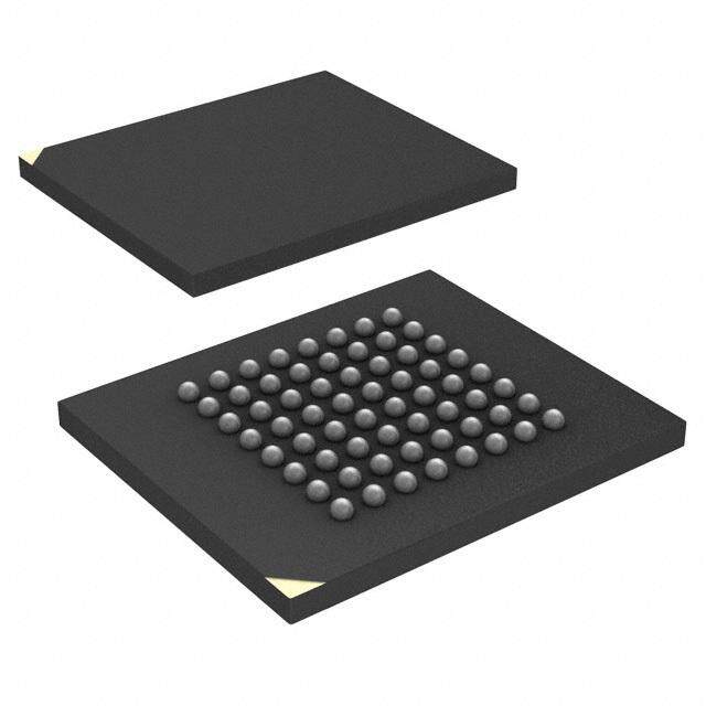
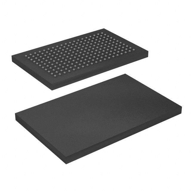
| 产品图片 |
|
| rohs | 符合RoHS无铅 / 符合限制有害物质指令(RoHS)规范要求 |
| 产品系列 | 内存,动态随机存取存储器,ISSI IS43R16160D-6TL- |
| 数据手册 | |
| 产品型号 | IS43R16160D-6TL |
| 产品种类 | 动态随机存取存储器 |
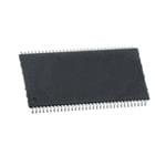
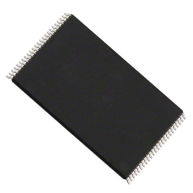
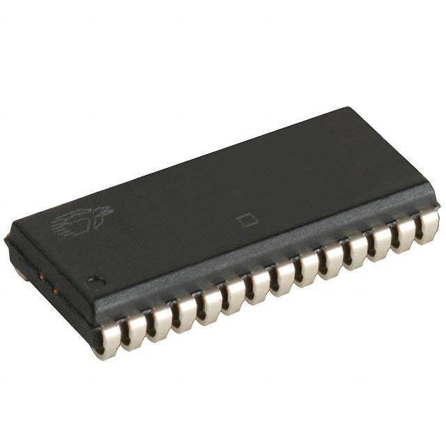
| 供应商器件封装 | 66-TSOP II |
| 其它名称 | 706-1171 |
| 包装 | 托盘 |
| 商标 | ISSI |
| 存储器类型 | DDR SDRAM |
| 存储容量 | 256 Mbit |
| 安装风格 | SMD/SMT |
| 封装 | Tray |
| 封装/外壳 | 66-TSSOP(0.400",10.16mm 宽) |
| 封装/箱体 | TSOP-66 |
| 工作温度 | 0°C ~ 70°C |
| 工厂包装数量 | 108 |
| 接口 | 并联 |
| 数据总线宽度 | 16 bit |
| 最大工作温度 | + 70 C |
| 最大工作电流 | 120 mA |
| 最大时钟频率 | 166 MHz |
| 最小工作温度 | 0 C |
| 标准包装 | 108 |
| 格式-存储器 | RAM |
| 电压-电源 | 2.3 V ~ 2.7 V |
| 电源电压-最大 | 2.7 V |
| 电源电压-最小 | 2.3 V |
| 类型 | DDR1 |
| 系列 | IS43R16160D |
| 组织 | 16 M x 16 |
| 访问时间 | 0.7 ns |
| 速度 | 166MHz |


- 商务部:美国ITC正式对集成电路等产品启动337调查
- 曝三星4nm工艺存在良率问题 高通将骁龙8 Gen1或转产台积电
- 太阳诱电将投资9.5亿元在常州建新厂生产MLCC 预计2023年完工
- 英特尔发布欧洲新工厂建设计划 深化IDM 2.0 战略
- 台积电先进制程称霸业界 有大客户加持明年业绩稳了
- 达到5530亿美元!SIA预计今年全球半导体销售额将创下新高
- 英特尔拟将自动驾驶子公司Mobileye上市 估值或超500亿美元
- 三星加码芯片和SET,合并消费电子和移动部门,撤换高东真等 CEO
- 三星电子宣布重大人事变动 还合并消费电子和移动部门
- 海关总署:前11个月进口集成电路产品价值2.52万亿元 增长14.8%


PDF Datasheet 数据手册内容提取
IS43R83200D IS43/46R16160D, IS43/46R32800D 8Mx32, 16Mx16, 32Mx8 JUNE 2012 256Mb DDR SDRAM FEATURES DEVICE OVERVIEW • VDD and VDDQ: 2.5V ± 0.2V ISSI’s 256-Mbit DDR SDRAM achieves high speed data • SSTL_2 compatible I/O transfer using pipeline architecture and two data word accesses per clock cycle. The 268,435,456-bit memory • Double-data rate architecture; two data transfers array is internally organized as four banks of 64Mb to per clock cycle allow concurrent operations. The pipeline allows Read • Bidirectional, data strobe (DQS) is transmitted/ and Write burst accesses to be virtually continuous, with received with data, to be used in capturing data the option to concatenate or truncate the bursts. The at the receiver programmable features of burst length, burst sequence • DQS is edge-aligned with data for READs and and CAS latency enable further advantages. The device centre-aligned with data for WRITEs is available in 8-bit, 16-bit and 32-bit data word size • Differential clock inputs (CK and CK) Input data is registered on the I/O pins on both edges • DLL aligns DQ and DQS transitions with CK of Data Strobe signal(s), while output data is referenced transitions to both edges of Data Strobe and both edges of CLK. • Commands entered on each positive CK edge; data Commands are registered on the positive edges of CLK. and data mask referenced to both edges of DQS An Auto Refresh mode is provided, along with a Self • Four internal banks for concurrent operation Refresh mode. All I/Os are SSTL_2 compatible. • Data Mask for write data. DM masks write data ADDRESS TABLE at both rising and falling edges of data strobe • Burst Length: 2, 4 and 8 Parameter 8M x 32 16M x 16 32M x 8 • Burst Type: Sequential and Interleave mode Configuration 2M x 32 x 4 4M x 16 x 4 8M x 8 x 4 • Programmable CAS latency: 2, 2.5 and 3 banks banks banks • Auto Refresh and Self Refresh Modes Bank Address BA0, BA1 BA0, BA1 BA0, BA1 • Auto Precharge Pins • TRAS Lockout supported (tRAP = tRCD) Autoprecharge A8/AP A10/AP A10/AP Pins Row Address 4K(A0 – A11) 8K(A0 – A12) 8K(A0 – A12) OPTIONS • Configuration(s): 8Mx32, 16Mx16, 32Mx8 Column 512(A0 – A7, 512(A0 – A8) 1K(A0 – A9) Address A9) • Package(s): 144 Ball BGA (x32) Refresh Count Com./Ind./A1 4K / 64ms 8K / 64ms 8K / 64ms 66-pin TSOP-II (x8, x16) and 60 Ball BGA (x8, x16) A2 4K / 16ms 8K / 16ms • Lead-free package available • Temperature Range: KEY TIMING PARAMETERS Commercial (0°C to +70°C) Speed Grade -5 -6 Units Industrial (-40°C to +85°C) Automotive, A1 (-40°C to +85°C) FCk Max CL = 3 200 167 MHz Automotive, A2 (-40°C to +105°C) FCk Max CL = 2.5 200 167 MHz FCk Max CL = 2 133 133 MHz Copyright © 2012 Integrated Silicon Solution, Inc. All rights reserved. ISSI reserves the right to make changes to this specification and its products at any time without notice. ISSI assumes no liability arising out of the application or use of any information, products or services described herein. Customers are advised to obtain the lat- est version of this device specification before relying on any published information and before placing orders for products. Integrated Silicon Solution, Inc. does not recommend the use of any of its products in life support applications where the failure or malfunction of the product can reason- ably be expected to cause failure of the life support system or to significantly affect its safety or effectiveness. Products are not authorized for use in such applications unless Integrated Silicon Solution, Inc. receives written assurance to its satisfaction, that: a.) the risk of injury or damage has been minimized; b.) the user assume all such risks; and c.) potential liability of Integrated Silicon Solution, Inc is adequately protected under the circumstances Integrated Silicon Solution, Inc. 1 Rev. B 06/19/2012
IS43R83200D IS43/46R16160D, IS43/46R32800D FUNCTIONAL BLOCK DIAGRAM (x32) CK COMMAND CK DECODER DM0-DM3 CKE & DATA IN 4 RCASS GECNLEORCATKOR 32 BUFFER 32 I/O 0-31 CAS REFRESH WE Mode Registers and CONTROLLER 4 DQS0-DQS3 Ext. Mode Registers SELF DATA OUT VDD/VDDQ REFRESH BUFFER Vss/VssQ A11 14 CONTROLLER 32 32 A10 A9 A8 REFRESH A7 COUNTER 2 A6 A5 4096 A4 12 ER 4096 BAAAAA32100 ADRDORWESS ULTIPLEXER ADRDORWESS 12 ROW DECOD 44009966 MEBMAAORNRRYKA YC 0ELL BA1 12 LATCH 12 M BUFFER 12 SENSE AMP I/O GATE 2 512 (x 32) COLUMN ADDRESS LATCH BANK CONTROL LOGIC 9 BURST COUNTER COLUMN DECODER COLUMN ADDRESS BUFFER 9 2 Integrated Silicon Solution, Inc. Rev. B 06/19/2012
IS43R83200D IS43/46R16160D, IS43/46R32800D FUNCTIONAL BLOCK DIAGRAM (x16) CK COMMAND CK DECODER LDM, UDM CKE & DATA IN 2 RCASS GECNLEORCATKOR 16 BUFFER 16 I/O 0-15 CAS REFRESH WE Mode Registers and CONTROLLER 2 LDQS, UDQS Ext. Mode Registers SELF DATA OUT VDD/VDDQ A12 REFRESH BUFFER Vss/VssQ A11 15 CONTROLLER 16 16 A10 A9 A8 REFRESH A7 COUNTER 2 A6 A5 8192 A4 13 ER 8192 BAAAAA32100 ADRDORWESS ULTIPLEXER ADRDORWESS 13 ROW DECOD 88119922 MEBMAAORNRRYKA YC 0ELL BA1 13 LATCH 13 M BUFFER 13 SENSE AMP I/O GATE 2 512 (x 16) COLUMN ADDRESS LATCH BANK CONTROL LOGIC 9 BURST COUNTER COLUMN DECODER COLUMN ADDRESS BUFFER 9 Integrated Silicon Solution, Inc. 3 Rev. B 06/19/2012
IS43R83200D IS43/46R16160D, IS43/46R32800D PIN CONFIGURATIONS 66 pin TSOP - Type II for x8 VDD 1 66 VSS DQ0 2 65 DQ7 VDDQ 3 64 VSSQ NC 4 63 NC DQ1 5 62 DQ6 VSSQ 6 61 VDDQ NC 7 60 NC DQ2 8 59 DQ5 VDDQ 9 58 VSSQ NC 10 57 NC DQ3 11 56 DQ4 VSSQ 12 55 VDDQ NC 13 54 NC NC 14 53 NC VDDQ 15 52 VSSQ NC 16 51 DQS NC 17 50 NC VDD 18 49 VREF NC 19 48 VSS NC 20 47 DM WE 21 46 CK CAS 22 45 CK RAS 23 44 CKE CS 24 43 NC NC 25 42 A12 BA0 26 41 A11 BA1 27 40 A9 A10/AP 28 39 A8 A0 29 38 A7 A1 30 37 A6 A2 31 36 A5 A3 32 35 A4 VDD 33 34 VSS PIN DESCRIPTION: x8 A0-A12 Row Address Input DM Data Write Mask A0-A9 Column Address Input DQS Data Strobe BA0, BA1 Bank Select Address VDD Power DQ0 – DQ7 Data I/O VDDQ Power Supply for I/O Pins CK, CK System Clock Input VSS Ground CKE Clock Enable VSSQ Ground for I/O Pins CS Chip Select VREF SSTL_2 reference voltage CAS Column Address Strobe NC No Connection Command RAS Row Address Strobe Command WE Write Enable 4 Integrated Silicon Solution, Inc. Rev. B 06/19/2012
IS43R83200D IS43/46R16160D, IS43/46R32800D PIN CONFIGURATION Package Code B: 60-ball FBGA (top view) for x8 (8mm x 13mm Body, 0.8mm Ball Pitch) Top View (Balls seen through the Package) :BallExisting 1 2 3 7 8 9 :DepopulatedBall TopView(SeetheballsthroughthePackage) VSSQ DQ7 VSS A VDD DQ0 VDDQ 1 2 3 4 5 6 7 8 9 NC VDDQ DQ6 B DQ1 VSSQ NC A NC VSSQ DQ5 C DQ2 VDDQ NC B NC VDDQ DQ4 D DQ3 VSSQ NC C D NC VSSQ DQS E NC VDDQ NC E VREF VSS DM F NC VDD NC F CK CK G WE CAS G H A12 CKE H RAS CS J A11 A9 J BA1 BA0 K A8 A7 K A0 A10/AP L M A6 A5 L A2 A1 A4 VSS M VDD A3 BGA Package Ball Pattern x8 DeviceBallPattern Top View PIN DESCRIPTION: x8 A0-A12 Row Address Input DQS Data Strobe A0-A9 Column Address Input VDD Power BA0, BA1 Bank Select Address VDDQ Power Supply for I/O Pins DQ0 – DQ7 Data I/O VSS Ground CK, CK System Clock Input VSSQ Ground for I/O Pins CKE Clock Enable VREF SSTL_2 reference voltage CS Chip Select NC No Connection CAS Column Address Strobe Command RAS Row Address Strobe Command WE Write Enable DM Data Write Mask Integrated Silicon Solution, Inc. 5 Rev. B 06/19/2012
IS43R83200D IS43/46R16160D, IS43/46R32800D PIN CONFIGURATIONS 66 pin TSOP - Type II for x16 VDD 1 66 VSS DQ0 2 65 DQ15 VDDQ 3 64 VSSQ DQ1 4 63 DQ14 DQ2 5 62 DQ13 VSSQ 6 61 VDDQ DQ3 7 60 DQ12 DQ4 8 59 DQ11 VDDQ 9 58 VSSQ DQ5 10 57 DQ10 DQ6 11 56 DQ9 VSSQ 12 55 VDDQ DQ7 13 54 DQ8 NC 14 53 NC VDDQ 15 52 VSSQ LDQS 16 51 UDQS NC 17 50 NC VDD 18 49 VREF NC 19 48 VSS LDM 20 47 UDM WE 21 46 CK CAS 22 45 CK RAS 23 44 CKE CS 24 43 NC NC 25 42 A12 BA0 26 41 A11 BA1 27 40 A9 A10/AP 28 39 A8 A0 29 38 A7 A1 30 37 A6 A2 31 36 A5 A3 32 35 A4 VDD 33 34 VSS PIN DESCRIPTION: x16 A0-A12 Row Address Input LDM, UDM Data Write Mask A0-A8 Column Address Input LDQS, UDQS Data Strobe BA0, BA1 Bank Select Address VDD Power DQ0 – DQ15 Data I/O VDDQ Power Supply for I/O Pins CK, CK System Clock Input VSS Ground CKE Clock Enable VSSQ Ground for I/O Pins CS Chip Select VREF SSTL_2 reference voltage CAS Column Address Strobe NC No Connection Command RAS Row Address Strobe Command WE Write Enable 6 Integrated Silicon Solution, Inc. Rev. B 06/19/2012
IS43R83200D IS43/46R16160D, IS43/46R32800D PIN CONFIGURATION Package Code B: 60-ball FBGA (top view) for x16 (8mm x 13mm Body, 0.8mm Ball Pitch) Top View (Balls seen through the Package) :BallExisting 1 2 3 7 8 9 :DepopulatedBall TopView(SeetheballsthroughthePackage) VSSQ DQ15 VSS A VDD DQ0 VDDQ 1 2 3 4 5 6 7 8 9 DQ14 VDDQ DQ13 B DQ2 VSSQ DQ1 A DQ12 VSSQ DQ11 C DQ4 VDDQ DQ3 B DQ10 VDDQ DQ9 D DQ6 VSSQ DQ5 C D DQ8 VSSQ UDQS E LDQS VDDQ DQ7 E VREF VSS UDM F LDM VDD NC F CK CK G WE CAS G H A12 CKE H RAS CS J A11 A9 J BA1 BA0 K A8 A7 K A0 A10/AP L M A6 A5 L A2 A1 A4 VSS M VDD A3 BGA Package Ball Pattern x16DeviceBallPattern Top View PIN DESCRIPTION: x16 A0-A12 Row Address Input LDQS, UDQS Data Strobe A0-A8 Column Address Input VDD Power BA0, BA1 Bank Select Address VDDQ Power Supply for I/O Pins DQ0 – DQ15 Data I/O VSS Ground CK, CK System Clock Input VSSQ Ground for I/O Pins CKE Clock Enable VREF SSTL_2 reference voltage CS Chip Select NC No Connection CAS Column Address Strobe Command RAS Row Address Strobe Command WE Write Enable LDM, UDM Data Write Mask Integrated Silicon Solution, Inc. 7 Rev. B 06/19/2012
IS43R83200D IS43/46R16160D, IS43/46R32800D PIN CONFIGURATION Package Code B: 144-ball FBGA (top view) (12mm x 12mm Body, 0.8mm Ball Pitch) Top View (Balls seen through the package) 1 2 3 4 5 6 7 8 9 10 11 12 A DQS0 DM0 VSSQ DQ3 DQ2 DQ0 DQ31 DQ29 DQ28 VSSQ DM3 DQS3 B DQ4 VDDQ NC VDDQ DQ1 VDDQVDDQ DQ30 VDDQ NC VDDQ DQ27 C DQ6 DQ5 VSSQ VSSQ VSSQ VDD VDD VSSQ VSSQ VSSQ DQ26 DQ25 D DQ7 VDDQ VDD VSS VSSQ VSS VSS VSSQ VSS VDD VDDQ DQ24 E DQ17 DQ16 VDDQ VSSQ VSS VSS VSS VSS VSSQ VDDQ DQ15 DQ14 F DQ19 DQ18 VDDQ VSSQ VSS VSS VSS VSS VSSQ VDDQ DQ13 DQ12 G DQS2 DM2 NC VSSQ VSS VSS VSS VSS VSSQ NC DM1 DQS1 H DQ21 DQ20 VDDQ VSSQ VSS VSS VSS VSS VSSQ VDDQ DQ11 DQ10 J DQ22 DQ23 VDDQ VSSQ VSS VSS VSS VSS VSSQ VDDQ DQ9 DQ8 K CAS WE VDD VSS A10 VDD VDD NC VSS VDD NC NC L RAS NC NC BA1 A2 A11 A9 A5 NC CK CK NC M CS NC BA0 A0 A1 A3 A4 A6 A7 A8 CKE VREF Note: Vss balls inside the dotted box are optional for purposes of thermal dissipation. PIN DESCRIPTION: for x32 A0-A11 Row Address Input WE Write Enable A0-A7, A9 Column Address Input DM0-DM3 Data Write Mask BA0, BA1 Bank Select Address DQS0-DQS3 Data Strobe DQ0 – DQ31 Data I/O VDD Power CK, CK System Clock Input VDDQ Power Supply for I/O Pins CKE Clock Enable VREF SSTL_2 reference voltage CS Chip Select VSS Ground CAS Column Address Strobe VSSQ Ground for I/O Pins Command NC No Connection RAS Row Address Strobe Command 8 Integrated Silicon Solution, Inc. Rev. B 06/19/2012
IS43R83200D IS43/46R16160D, IS43/46R32800D PIN FUNCTIONAL DESCRIPTIONS Symbol Type Description CK, CK Input Clock: CK and CK are differential clock inputs. All address and control input signals are sampled on the crossing of the positive edge of CK and negative edge of CK. Input and output data is referenced to the crossing of CK and CK (both directions of crossing). Internal clock signals are derived from CK/ CK. CKE Input Clock Enable: CKE HIGH activates, and CKE LOW deactivates internal clock signals, and device input buffers and output drivers. Taking CKE LOW provides PRECHARGE POWER-DOWN and SELF REFRESH operation (all banks idle), or ACTIVE POWERDOWN (row ACTIVE in any bank). CKE is synchronous for all functions except for SELF REFRESH EXIT, which is achieved asynchronously. Input buffers, excluding CK, CK and CKE, are disabled during power-down and self refresh mode which are contrived for low standby power consumption. CS Input Chip Select: CS enables (registered LOW) and disables (registered HIGH) the command decoder. All commands are masked when CS is registered HIGH. CS provides for external bank selection on systems with multiple banks. CS is considered part of the command code. RAS, CAS, Input Command Inputs: RAS, CAS and WE (along with CS) define the command being entered. WE DM: x8; Input Input Data Mask: DM is an input mask signal for write data. Input data is masked when DM is LDM, UDM: sampled HIGH along with that input data during a WRITE access. DM is sampled on both edges x16; of DQS. Although DM pins are input-only, the DM loading matches the DQ and DQS loading. DM0-DM3: For x16 devices, LDM corresponds to the data on DQ0-DQ7, UDM corresponds to the data on x32 DQ8-DQ15. For x32 devices, DM0 corresponds to the data on DQ0-DQ7, DM1 corresponds to the data on DQ8-DQ15, DM2 corresponds to the data on DQ16-DQ23, and DM3 corresponds to the data on DQ24-DQ31. BA0, BA1 Input Input Bank Address Inputs: BA0 and BA1 define to which bank an ACTIVE, READ, WRITE or PRECHARGE command is being applied. A [12:0] Input Address Inputs: provide the row address for ACTIVE commands, and the column address and AUTO PRECHARGE bit for READ / WRITE commands, to select one location out of the memory array in the respective bank. The address inputs also provide the opcode during a MODE REGISTER SET command. A12 is not used for x32. DQ: I/O Data Bus: Input / Output DQ0-DQ7: x8; DQ0-DQ15: x16 DQ0-DQ31: x32 DQS: x8: I/O Data Strobe: Output with read data, input with write data. Edge-aligned with read data, centered with write data. Used to capture write data. LDQS, UDQS x16: For x16 device, LDQS corresponds to the data on DQ0-DQ7, UDQS corresponds to the data on DQS0-DQS3: DQ8-DQ15. x32 For x32 device, DQS0 corresponds to the data on DQ0-DQ7, DQS1 corresponds to the data on DQ8-DQ15, DQS2 corresponds to the data on DQ16-DQ23, and DQS3 corresponds to the data on DQ24-DQ31. NC -- No Connect: Should be left unconnected. VREF Supply SSTL_2 reference voltage. VDDQ Supply I/O Power Supply. VSSQ Supply I/O Ground. VDD Supply Power Supply. VSS Supply Ground. Integrated Silicon Solution, Inc. 9 Rev. B 06/19/2012
IS43R83200D IS43/46R16160D, IS43/46R32800D COMMANDS TRUTH TABLES All commands (address and control signals) are registered on the positive edge of clock (crossing of CK going high and CK going low). Truth Table shows basic timing parameters for all commands. TRUTH TABLE - COMMANDS NAME (FUNCTION) CS RAS CAS WE BA AP Address Notes DESELECT (NOP) H X X X X X X 2 NO OPERATION (NOP) L H H H X X X 2 ACTIVE (select bank and activate row) L L H H Valid X Row READ (select bank and column and start read L H L H Valid L Column burst) READ with AP (read burst with Auto Precharge) L H L H Valid H Column 3 WRITE (select bank and column and start write L H L L Valid L Column burst) WRITE with AP (write burst with Auto L H L L Valid H Column 3 Precharge) BURST TERMINATE L H H L X X X 4 PRECHARGE (deactivate row in selected L L H L Valid L X 5 bank) PRECHARGE ALL (deactivate rows in all L L H L X H X 5 banks) AUTO REFRESH or enter SELF REFRESH L L L H X X X 6,7,8 MODE REGISTER SET L L L L Valid Op-code 9 Notes: 1. All states and sequences not shown are illegal or reserved. 2. DESELECT and NOP are functionally interchangeable. 3. Autoprecharge is non-persistent. AP High enables Auto Precharge, while AP Low disables Autoprecharge. 4. Burst Terminate applies to only Read bursts with Auto Precharge disabled. This command is undefined and should not be used for Read with Auto Precharge enabled, and for Write bursts. 5. If AP is Low, bank address determines which bank is to be precharged. If AP is High, all banks are precharged and BA0- BA1are don’t care. 6. This command is AUTO REFRESH if CKE is High, and SELF REFRESH if CKE is low. 7. All address inputs and I/O are ‘don't care’ except for CKE. Internal refresh counters control bank and row addressing. 8. All banks must be precharged before issuing an AUTO-REFRESH or SELF REFRESH command. 9. BA0 and BA1 value select between MRS and EMRS. 10. CKE is HIGH for all commands shown except SELF REFRESH. TRUTH TABLE - DM Operations ADDRESSING FUNCTION DM DQ x32 x16 x8 Write Enable L Valid Auto Precharge (AP) A8 A10 A10 Write Inhibit H X Row Address (RA) A0-A11 A0-A12 A0-A12 Column Address (CA) A0-A7, A0-A8 A0-A9 Note: Used to mask write data, provided coincident with the corresponding data. A9 10 Integrated Silicon Solution, Inc. Rev. B 06/19/2012
IS43R83200D IS43/46R16160D, IS43/46R32800D TRUTH TABLE - CKE CKE n-1 CKE n Current State COMMAND n ACTION n NOTES L L Power Down X Maintain Power Down L L Self Refresh X Maintain Self Refresh L H Power Down NOP or DESELECT Exit Power Down 6 L H Self Refresh NOP or DESELECT Exit Self Refresh 6, 7 H L All Banks Idle NOP or DESELECT Precharge Power Down Entry 6 H L Bank(s) Active NOP or DESELECT Active Power Down Entry 6 H L All Banks Idle AUTO REFRESH Self Refresh entry H H See Truth Tables - Commands Notes: 1. CKEn is the logic state of CKE at clock edge n; CKEn-1 was the state of CKE at the previous clock edge. 2. Current state is the state of DDR immediately prior to clock edge n. 3. COMMANDn is the command registered at clock edge n, and ACTIONn is the result of COMMANDn. 4. All states and sequences not shown are illegal or reserved. 5. CKE must not go LOW during a Read or Write, and must stay HIGH until after tRPSt or twR, respectively. 6. DESELECT and NOP are functionally interchangeable. 7. NOPs or Deselects must be issued for at least tSnR after Self-Refresh exit before any other command. After DLL Reset, at least txSRD must elapse before any Read commands occur. Basic Timing Parameters for Commands t t t CK CH CL CK CK t t IS IH Input Valid Valid Valid = Don't Care NOTE: Input = A0 - An, BA0, BA1, CKE, CS, RAS, CAS, WE; An = Address bus MSB ADDRESSING Integrated Silicon Solution, Inc. 11 Rev. B 06/19/2012
IS43R83200D IS43/46R16160D, IS43/46R32800D SIMPLIFIED STATE DIAGRAM Power Applied Power On Precharge PREALL Self Refresh REFS REFSX MRS MRS REFA Auto EMRS Idle Refresh CKEL CKEH Active Power ACT Down Precharge Power Down CKEH CKEL BurstStop Row Write Active Read Write Read WriteA ReadA Write Read Read WriteA ReadA Read A PRE Write Read A PRE PRE A Precharge PRE PREALL AutomaticSequence CommandSequence PREALL = Precharge All Banks REFS = Enter Self Refresh CKEL = Enter Power Down Write A = Write with Autoprecharge MRS = Mode Register Set REFSX = Exit Self Refresh CKEH = Exit Power Down Read A = Read with Autoprecharge EMRS = Extended Mode Register Set REFA = Auto Refresh ACT = Active PRE = Precharge 12 Integrated Silicon Solution, Inc. Rev. B 06/19/2012
IS43R83200D IS43/46R16160D, IS43/46R32800D FUNCTIONAL DESCRIPTION The DDR SDRAM is a high speed CMOS, dynamic random-access memory internally configured as a quad-bank DRAM. The 256Mb devices contains: 268,435,456 bits. The DDR SDRAM uses double data rate architecture to achieve high speed operation. The double data rate architecture is essentially a 2n prefetch architecture with an interface designed to transfer two data words per clock cycle at the I/O pins. A single read or write access for the DDR SDRAM effectively consists of a single 2n-bit wide, one clock cycle data transfer at the internal DRAM core and two corresponding n-bit wide, one-half-clock-cycle data transfers at the I/O pins. Read and write accesses to the DDR SDRAM are burst oriented; accesses start at a selected location and continue for a programmed number of locations in a programmed sequence. Accesses begin with the registration of an ACTIVE command, which is then followed by a READ or WRITE command. The address bits registered coincident with the ACTIVE command are used to select the bank and the row to be accessed. The address bits registered coincident with the READ or WRITE command are used to select the bank and the starting column location for the burst access. Prior to normal operation, the DDR SDRAM must be initialized. The following section provides detailed information covering device initialization, register definition, command description and device operation INITIALIZATION DDR SDRAMs must be powered up and initialized in a predefined manner. Operations procedures other than those specified may result in undefined operation. If there is any interruption to the device power, the initialization routine should be followed. The steps to be followed for device initialization are listed below. The Initialization Flow diagram and the Initialization Flow sequence are shown in the following figures. The Mode Register and Extended Mode Register do not have default values. If they are not programmed during the initialization sequence, it may lead to unspecified operation. The clock stop feature is not available until the device has been properly initialized from Step 1 through 13. • Step 1: Apply VDD before or at the same time as VDDQ. • Step 2: CKE must maintain LVCMOS Low until VREF is stable. Apply VDDQ before applying VTT and VREF. • Step 3: There must be at least 200 μs of valid clocks before any command may be given to the DRAM. During this time NOP or DESELECT commands must be issued on the command bus and CKE should be brought HIGH. • Step 4: Issue a PRECHARGE ALL command. • Step 5: Provide NOPs or DESELECT commands for at least tRP time. • Step 6: Issue EMRS command • Step 7: Issue MRS command, load the base mode register and to reset the DLL. Set the desired operating modes. • Step 8: Provide NOPs or DESELECT commands for at least tMRD time. • Step 9: Issue a PRECHARGE ALL command • Step 10: Issue 2 or more AUTO REFRESH cycles • Step 11: Issue MRS command with the reset DLL bit deactivated to program operating parameters without resetting the DLL • Step 12: Provide NOP or DESELECT commands for at least tMRD time. • Step 13: The DRAM has been properly initialized and is ready for any valid command. Integrated Silicon Solution, Inc. 13 Rev. B 06/19/2012
IS43R83200D IS43/46R16160D, IS43/46R32800D Initialization Waveform Sequence VDD VDDQ tVDT≥ 0 VTT (system1) VREF tCK tCH tCL CK (( (( (( (( (( (( )) )) )) )) )) )) CK (( (( (( (( (( (( )) )) )) )) )) )) tIS tIH (( (( (( (( (( CKE LVCMOSLOWLEVEL()() ())()) ())()) ())()) ())()) ())()) tIS tIH (( (( (( (( (( (( )) )) )) )) )) )) COMMAND (( NOP PRE EMRS (( MRS (( PRE (( AR (( AR (( MRS ACT )) )) )) )) )) )) (( (( (( (( (( (( DM )) )) )) )) )) )) (( (( (( (( (( (( )) )) )) )) )) )) tIS tIH ()() ()() ()() ()() ()() ()() Address ()() CODE ()() CODE ()() ()() ()() ()() CODE RA tIS tIH AP4 ()()(()) ALLBANKS CODE ()()()() CODE ()()()() ALLBANKS ()()(()) (())(()) ()()()() CODE RA tIS tIH tIS tIH tIS tIH (( (( (( (( (( (( BA0,BA1 )) BA0=H, )) BA0=L, )) )) )) )) BA0=L, BA (( BA1=L (( BA1=L (( (( (( (( BA1=L )) )) )) )) )) )) DQS ()() High--Z ()() ()() ()() ()() ()() DQ (( High--Z (( (( (( (( (( )) )) )) )) )) )) T=200µs tMRD2 tMRD2 tRP tRFC tRFC tMRD2 Power--up: Extended 200cyclesofCK** VDDand Mode Load CLKstable Register Mode Set Load Register Mode (withAP=L) Register, ResetDLL DON’TCARE (withAP=H) Notes: 1. VTT is not applied directly to the device, however tVTD must be greater than or equal to zero to avoid device latch--up. 2. tMRD is required before any command can be applied, and 200 cycles of CK are required before any executable command can be applied 3. The two Auto Refresh commands may be moved to follow the first MRS but precede the second PRECHARGE ALL com- mand. 4. AP is A8 for x32, and A10 for x8/x16. Address is A0 to A12 except AP. 14 Integrated Silicon Solution, Inc. Rev. B 06/19/2012
IS43R83200D IS43/46R16160D, IS43/46R32800D MODE REGISTER (MR) DEFINITION The Mode Register is used to define the specific mode of operation of the DDR SDRAM. This definition includes the definition of a burst length, a burst type, and a CAS latency. The Mode Register is programmed via the MODE REGISTER SET command (with BA0=0 and BA1=0) and will retain the stored information until it is reprogrammed, or the device loses power. Mode Register bits A0-A2 specify the burst length, A3 the type of burst (sequential or interleave), A4-A6 the CAS latency, and A8 DLL reset. A logic 0 should be programmed to all the undefined addresses bits to ensure future compatibility. The Mode Register must be loaded when all banks are idle and no bursts are in progress, and the controller must wait the specified time tMRD before initiating any subsequent operation. Violating either of these requirements will result in unspecified operation. Reserved states should not be used, as unknown operation or incompatibility with future versions may result MODE REGISTER Address Bus (Ax) BA1 BA0 A121 A11 A10 A9 A8 A7 A6 A5 A4 A3 A2 A1 A0 Mode Reg. (Ex) A2 A1 A0 Burst Length 0 0 0 Reserved 0 0 1 2 0 1 0 4 0 1 1 8 1 0 0 Reserved 1 0 1 Reserved 1 1 0 Reserved 1 1 1 Reserved A3 Burst Type 0 Sequential 1 Interleave A6 A5 A4 CAS Latency 0 0 0 Reserved 0 0 1 Reserved 0 1 0 2 A12 A11 A10 A9 A8 A7 DLL 0 1 1 3 0 0 0 0 0 0 Normal operation 1 0 0 Reserved 0 0 0 0 1 0 Reset DLL 1 0 1 Reserved 1 1 0 2.5 1 1 1 Reserved BA1 BA0 Mode Register Definition 0 0 Program Mode Register 0 1 Program Extended Mode Register Notes: 1 0 Reserved 1. A12 is not used in x32 and should be ignored for this option. 1 1 Reserved 2. A logic 0 should be programmed to all unused / undefined address bits to ensure future compatibility. Integrated Silicon Solution, Inc. 15 Rev. B 06/19/2012
IS43R83200D IS43/46R16160D, IS43/46R32800D BURST LENGTH Read and write accesses to the DDR SDRAM are burst oriented, with the burst length being set and the burst order as in Burst Definition. The burst length determines the maximum number of column locations that can be accessed for a given READ or WRITE command. Burst lengths of 2, 4, or 8 locations are available for both the sequential and the interleaved burst types. BURST DEFINITION Burst Starting Column Address Order of Accesses Within a Burst Length Type = Sequential Type = Interleaved A0 2 0 0-1 0-1 1 1-0 1-0 A1 A0 0 0 0-1-2-3 0-1-2-3 4 0 1 1-2-3-0 1-0-3-2 1 0 2-3-0-1 2-3-0-1 1 1 3-0-1-2 3-2-1-0 A2 A1 A0 0 0 0 0-1-2-3-4-5-6-7 0-1-2-3-4-5-6-7 0 0 1 1-2-3-4-5-6-7-0 1-0-3-2-5-4-7-6 0 1 0 2-3-4-5-6-7-0-1 2-3-0-1-6-7-4-5 8 0 1 1 3-4-5-6-7-0-1-2 3-2-1-0-7-6-5-4 1 0 0 4-5-6-7-0-1-2-3 4-5-6-7-0-1-2-3 1 0 1 5-6-7-0-1-2-3-4 5-4-7-6-1-0-3-2 1 1 0 6-7-0-1-2-3-4-5 6-7-4-5-2-3-0-1 1 1 1 7-0-1-2-3-4-5-6 7-6-5-4-3-2-1-0 Notes: 1. For a burst length of two, A1-An selects the two data element block; A0 selects the first access within the block. 2. For a burst length of four, A2-An selects the four data element block; A0-A1 selects the first access within the block. 3. For a burst length of eight, A3-An selects the eight data element block; A0-A2 selects the first access within the block. 4. Whenever a boundary of the block is reached within a given sequence, the following access wraps within the block. 16 Integrated Silicon Solution, Inc. Rev. B 06/19/2012
IS43R83200D IS43/46R16160D, IS43/46R32800D When a READ or WRITE command is issued, a block of columns equal to the burst length is effectively selected. All accesses for that burst take place within the block, meaning that the burst will wrap within the block if a boundary is reached. The block is uniquely selected by A1-An when the burst length is set to two, by A2-An when the burst length is set to 4, by A3-An when the burst length is set to 8. An is the most significant column address bit, which depends if the device is x8, x16 or x32. An = A9 for x8, An = A8 for x16 and An = A9 for x32. The programmed burst length applies to both read and write bursts. BURST TYPE Accesses within a given burst may be programmed to be either sequential or interleaved; this is referred to as the burst type and is selected via bit A3. The ordering of accesses within a burst is determined by the burst length, the burst type and the starting column address. READ LATENCY The READ latency, or CAS latency, is the delay between the registration of a READ command and the availability of the first piece of output data. If a READ command is registered at a clock edge n and the latency is 3 clocks, the first data element will be valid at n + 2tCK + tAC. If a READ command is registered at a clock edge n and the latency is 2 clocks, the first data element will be valid at n + tCK + tAC. OPERATING MODE The normal operating mode is selected by issuing a Mode Register Set command with bits A7 to An each set to zero, and bits A0 to A6 set to the desired values. A DLL reset is initiated by issuing a Mode Register Set command with bits A7 and A9 to An each set to zero, bit A8 set to one, and bits A0 to A6 set to the desired values. A Mode Register Set command issued to reset the DLL must always be followed by a Mode Register Set command to select normal operating mode (A8=0). All other combinations of values for A7 to An are reserved for future use and/or test modes. Test modes and reserved states should not be used because unknown operation or incompatibility with future versions may result. Integrated Silicon Solution, Inc. 17 Rev. B 06/19/2012
IS43R83200D IS43/46R16160D, IS43/46R32800D CAS LATENCIES 18 Integrated Silicon Solution, Inc. Rev. B 06/19/2012
IS43R83200D IS43/46R16160D, IS43/46R32800D EXTENDED MODE REGISTER (EMR) DEFINITION The Extended Mode Register controls functions beyond those controlled by the Mode Register; these additional functions include DLL enable/disable, and output drive strength selection. The Extended Mode Register is programmed via the MODE REGISTER SET command (with BA1=0 and BA0=1) and will retain the stored information until it is reprogrammed, or the device loses power. The Extended Mode Register must be loaded when all banks are idle and no bursts are in progress, and the controller must wait the specified time tMRD before initiating any subsequent operation. Violating either of these requirements will result in unspecified operation. Reserved states should not be used, as unknown operation or incompatibility with future versions may result. DLL Enable/Disable The DLL must be enabled for normal operation. DLL enable is required during power-up initialization, and upon returning to normal operation after having disabled the DLL for the purpose of debug or evaluation (upon exiting Self Refresh Mode, the DLL is enabled automatically). Any time the DLL is enabled a DLL Reset must follow and 200 clock cycles must occur before any executable command can be issued. OUTPUT DRIVE STRENGTH (DS) The normal drive strength for all outputs is specified to be SSTL_2, Class II. This DRAM also supports a reduced driver strength option, intended for lighter load and/or point-to-point environments. EXTENDED MODE REGISTER BA1 BA0 A122 A11 A10 A9 A8 A7 A6 A5 A4 A3 A2 A1 A0 Address Bus (Ax) Ext. Mode Reg. (Ex) Reserved(1) A0 DLL 0 Enable 1 Disable A1 Drive Strength 0 Normal 1 Reduced BA1 BA0 Mode Register Definition NOTES: 0 0 Program Mode Register 1. A logic 0 should be programmed to all unused/undefined ad- dress bits to ensure future compatibility 0 1 Program Extended Mode Register 2. A12 is not used for x32 and should be ignored for this option. 1 0 Reserved 1 1 Reserved Integrated Silicon Solution, Inc. 19 Rev. B 06/19/2012
IS43R83200D IS43/46R16160D, IS43/46R32800D Absolute Maximum Rating Parameter Symbol Value Unit Voltage on any pin relative to VSS Vin, Vout -1.0 ~ 3.6 V Voltage on VDD & VDDQ supply relative to VSS VDD, VDDq -1.0 ~ 3.6 V Storage temperature TStg -55 ~ +150 oC Power dissipation PD 1.5 W Short circuit current IoS 50 mA Note: Permanent device damage may occur if ABSOLUTE MAXIMUM RATINGS are exceeded. Functional operation should be restricted to recommend operation condition. Exposure to higher than recommended voltage for extended periods of time could affect device reliability AC/DC Electrical Characteristics and Operating Conditions Recommended operating conditions (Voltage referenced to VSS=0V; TA=0 to 70oC for Commercial, TA = -40oC to +85oC for Industrial and A1, TA = -40oC to +105oC for A2) Parameter Symbol Min Max Unit Note Supply voltage (with a nominal VDD of 2.5V) VDD 2.3 2.7 V I/O Supply voltage (with a nominal VDD of 2.5V) VDDq 2.3 2.7 V I/O Reference voltage VRef 0.49*VDDQ 0.51*VDDQ V 1 I/O Termination voltage (system) Vtt VREF-0.04 VREF+0.04 V 2 Input logic high voltage Vih(DC) VREF+0.15 VDDQ+0.3 V Input logic low voltage Vil(DC) -0.3 VREF-0.15 V Input Voltage Level, CLK and CLK inputs Vin(DC) -0.3 VDDQ+0.3 V Input Differential Voltage, CLK and CLK inputs ViD(DC) 0.36 VDDQ+0.6 V 3 V-I Matching: Pullup to Pulldown Current Ratio Vi(Ratio) 0.71 1.4 – 4 Input leakage current Il -2 2 uA Output leakage current Ioz -5 5 uA Output High Current (Normal strength driver) ; VOUT = VTT + 0.84V Ioh -16.8 – mA Output Low Current (Normal strength driver) ; VOUT = VTT - 0.84V Iol 16.8 – mA Output High Current (Half strength driver); VOUT = VTT + 0.45V IohR -9 – mA Output Low Current (Half strength driver); VOUT = VTT - 0.45V IolR 9 – mA Ambient Operating Temperature Commercial TA 0 +70 oC Industrial TA -40 +85 oC A1 TA -40 +85 oC A2 TA -40 +105 oC Note : 1. VREF is expected to be equal to 0.5*VDDQ of the transmitting device, and to track variations in the dc level of same. Peak-to peak noise on VREF may not exceed +/-2% of the dc value. 2. VTT is not applied directly to the device. VTT is a system supply for signal termination resistors, is expected to be set equal to VREF, and must track variations in the DC level of VREF 3. VID is the magnitude of the difference between the input level on CLK and the input level on CLK. 4. The ratio of the pullup current to the pulldown current is specified for the same temperature and voltage, over the entire tem- perature and voltage range, for device drain to source voltages from 0.25V to 1.0V. For a given output, it represents the maxi- mum difference between pullup and pulldown drivers due to process variation. The full variation in the ratio of the maximum to minimum pullup and pulldown current will not exceed 1.7 for device drain to source voltages from 0.1 to 1.0. 20 Integrated Silicon Solution, Inc. Rev. B 06/19/2012
IS43R83200D IS43/46R16160D, IS43/46R32800D CAPACITANCE CHARACTERISTICS(1, 2) (VDD = VDDq = 2.5V + 0.2V, unless otherwise noted) Symbol Parameter Test Condition Limits Units Min Max CI(A) Input Capacitance, address pin VI=1.25v 1.3 3 pF CI(C) Input Capacitance, control pin f=100MHz 1.3 3 pF CI(K) Input Capacitance, CLK pin VI=25mVrms 1.3 3 pF CI/O I/O Capacitance, I/O, DQS, DM pin 3 5 pF Notes: 1. This parameter is characterized. 2. Conditions: Frequency = 100MHz; Vout(DC) = VDD/2; Vout(peak-to-peak) = 0.2V; VRef = Vss. THERMAL RESISTANCE Package Substrate Theta-ja Theta-ja Theta-ja Theta-jc Units (Airflow = 0m/s) (Airflow = 1m/s) (Airflow = 2m/s) TSOP2(66) 4-layer 69.7 61.2 57.5 12.7 C/W BGA(60) 4-layer 40.1 36.5 34.2 7.9 C/W BGA(144) 4-layer 29.4 29 27.1 4.5 C/W Integrated Silicon Solution, Inc. 21 Rev. B 06/19/2012
IS43R83200D IS43/46R16160D, IS43/46R32800D IDD Specification Parameters and Test Conditions: x8, x16 (VDD = VDDq = 2.5V ± 0.2V, Vss = VssQ = 0V, Output Open, unless otherwise noted) Symbol Parameter/ Test Condition -5 -6 Units IDD0 Operating current for one bank active-precharge; tRC = tRC(min); 130 120 mA tCK = tCK(min); DQ, DM and DQS inputs changing once per clock cycle; address and control inputs changing once every two clock cycles; CS = high between valid commands. IDD1 Operating current for one bank operation; one bank open, BL = 4, 140 130 mA tRC = tRC(min), tCK = tCK(min), Iout=0mA, Address and control inputs changing once per clock cycle. IDD2P Precharge power-down standby current; all banks idle; power-down 30 30 mA mode; CKE VIL(max); tCK = tCK(min); VIN = VREF for DQ, DQS and DM IDD2F Precharge floating standby current; CS VIH(min); all banks idle; CKE 60 60 mA VIH(min); tCK = tCK(min); address and other control inputs changing once per clock cycle; VIN = VREF for DQ, DQS and DM IDD3P Active power-down standby current; one bank active; power-down 35 35 mA mode; CKE VIL(max); tCK = tCK(min); VIN = VREF for DQ, DQS and DM IDD3N Active standby current; CS VIH(min); CKE VIH(min); one bank 75 75 mA active; tRC = tRAS(max); tCK = tCK(min); DQ, DQS and DM inputs changing twice per clock cycle; address and other control inputs changing once per clock cycle IDD4R Operating current for burst read; burst length = 2; reads; continuous 240 210 mA burst; one bank active; address and control inputs changing once per clock cycle; tCK = tCK(min); 50% of data changing on every transfer; lOUT = 0mA IDD4W Operating current for burst write; burst length = 2; writes; continuous 260 220 mA burst; one bank active address and control inputs changing once per clock cycle; tCK = tCK(min); DQ, DM and DQS inputs changing twice per clock cycle, 50% of input data changing at every transfer IDD5 Auto refresh current; tRC = tRFC(min); 140 140 mA IDD6 Self refresh current; CKE 0.2V; 10 10 mA IDD7 Operating current for four bank operation; four bank interleaving 330 280 mA READs (BL=4) with auto precharge; tRC = tRC(min), tCK = tCK(min); Address and control inputs change only during ACTIVE, READ, or WRITE commands 22 Integrated Silicon Solution, Inc. Rev. B 06/19/2012
IS43R83200D IS43/46R16160D, IS43/46R32800D IDD Specification Parameters and Test Conditions: x32 (VDD = VDDq = 2.5V ± 0.2V, Vss = VssQ = 0V, Output Open, unless otherwise noted) Symbol Parameter/ Test Condition -5 -6 Units IDD0 Operating current for one bank active-precharge; tRC = tRC(min); 180 160 mA tCK = tCK(min); DQ, DM and DQS inputs changing once per clock cycle; address and control inputs changing once every two clock cycles; CS = high between valid commands. IDD1 Operating current for one bank operation; one bank open, BL = 4, 190 170 mA tRC = tRC(min), tCK = tCK(min), Iout=0mA, Address and control inputs changing once per clock cycle. IDD2P Precharge power-down standby current; all banks idle; power-down 35 35 mA mode; CKE VIL(max); tCK = tCK(min); VIN = VREF for DQ, DQS and DM IDD2F Precharge floating standby current; CS VIH(min); all banks idle; CKE 65 65 mA VIH(min); tCK = tCK(min); address and other control inputs changing once per clock cycle; VIN = VREF for DQ, DQS and DM IDD3P Active power-down standby current; one bank active; power-down 45 45 mA mode; CKE VIL(max); tCK = tCK(min); VIN = VREF for DQ, DQS and DM IDD3N Active standby current; CS VIH(min); CKE VIH(min); one bank 80 80 mA active; tRC = tRAS(max); tCK = tCK(min); DQ, DQS and DM inputs changing twice per clock cycle; address and other control inputs changing once per clock cycle IDD4R Operating current for burst read; burst length = 2; reads; continuous 330 300 mA burst; one bank active; address and control inputs changing once per clock cycle; tCK = tCK(min); 50% of data changing on every transfer; lOUT = 0mA IDD4W Operating current for burst write; burst length = 2; writes; continuous 340 310 mA burst; one bank active address and control inputs changing once per clock cycle; tCK = tCK(min); DQ, DM and DQS inputs changing twice per clock cycle, 50% of input data changing at every transfer IDD5 Auto refresh current; tRC = tRFC(min); 220 220 mA IDD6 Self refresh current; CKE 0.2V; 10 10 mA IDD7 Operating current for four bank operation; four bank interleaving 460 430 mA READs (BL=4) with auto precharge; tRC = tRC(min), tCK = tCK(min); Address and control inputs change only during ACTIVE, READ, or WRITE commands Integrated Silicon Solution, Inc. 23 Rev. B 06/19/2012
IS43R83200D IS43/46R16160D, IS43/46R32800D AC TIMING REQUIREMENTS Absolute Specifications (VDD, VDDQ = +2.5 V ±0.2 V) PARAMETER SYMBOL -5 -6 UNITS MIN MAX MIN MAX DQ output access time for CLK,/CLK tAC -0.7 0.7 -0.7 0.7 ns DQS output access time for CLK,/CLK tDQSCK -0.6 0.6 -0.6 0.6 ns CLK high-level width tCH 0.45 0.55 0.45 0.55 tCK CLK low-level width tCL 0.45 0.55 0.45 0.55 tCK CLK half period tHP min – min – ns (tCL,tCH) (tCL,tCH) CLK cycle time CL=3 tCK(3) 5 12 6 12 ns CL=2.5 tCK(2.5) 5 12 6 12 ns CL=2 tCK(2) 7.5 12 7.5 12 ns DQ and DM input hold time tDH 0.4 – 0.45 – ns DQ and DM input setup time tDS 0.4 – 0.45 – ns Control & Address input pulse width (for each tIPW 2.2 – 2.2 – ns input) DQ and DM input pulse width (for each input) tDIPW 1.75 – 1.75 – ns DQ & DQS high-impedance time from CLK,/CLK tHZ – 0.7 – 0.7 ns DQ & DQS low--impedance time from CLK,/CLK tLZ -0.7 – -0.7 – ns DQS--DQ Skew, DQS to last DQ valid, per group, tDQSQ – 0.4 – 0.45 ns per access DQ/DQS output hold time from DQS tQH tHP-tQHS – tHP- – ns tQHS Data Hold Skew Factor tQHS – 0.5 – 0.55 ns Write command to first DQS latching transition tDQSS 0.72 1.28 0.75 1.28 tCK DQS input high pulse width tDQSH 0.35 – 0.35 – tCK DQS input low pulse width tDQSL 0.35 – 0.35 – tCK DQS falling edge to CLK setup time tDSS 0.2 – 0.2 – tCK DQS falling edge hold time from CLK tDSH 0.2 – 0.2 – tCK MODE REGISTER SET command cycle time tMRD 2 – 2 – tCK Write preamble setup time tWPRES 0 – 0 – ns Write postamble tWPST 0.4 0.6 0.4 0.6 tCK Write preamble tWPRE 0.25 – 0.25 – tCK Address and Control input hold time (fast slew tIHF 0.6 – 0.75 – ns rate) Address and Control input setup time (fast slew tISF 0.6 – 0.75 – ns rate) Address and Control input hold time (slow slew tIH 0.7 – 0.8 -– ns rate) Address and Control input setup time (slow slew tIS 0.7 – 0.8 – ns rate) Read preamble tRPRE 0.9 1.1 0.9 1.1 tCK Read postamble tRPST 0.4 0.6 0.4 0.6 tCK ACTIVE to PRECHARGE command tRAS 40 70,000 42 120,000 ns 24 Integrated Silicon Solution, Inc. Rev. B 06/19/2012
IS43R83200D IS43/46R16160D, IS43/46R32800D AC TIMING REQUIREMENTS Absolute Specifications (VDD, VDDQ = +2.5 V ±0.2 V@-5/-6) PARAMETER SYMBOL -5 -6 UNITS MIN MAX MIN MAX ACTIVE to ACTIVE/Auto Refresh command tRC 55 – 60 – ns period Auto Refresh to Active/Auto tRFC 70 – 72 – ns ACTIVE to READ or WRITE delay tRCD 15 – 15 – ns PRECHARGE command period tRP 15 – 15 – ns Active to Autoprecharge Delay tRAP 15 – 15 – ns ACTIVE bank A to ACTIVE bank B command tRRD 10 – 12 – ns Write recovery time tWR 15 – 15 – ns Auto Precharge write recovery + precharge time tDAL tWR+tRP – tWR+tRP – tCK Internal Write to Read Command Delay tWTR 2 – 1 – tCK Exit self refresh to non-READ tXSNR 70 – 75 – ns Exit self refresh to READ command tXSRD 200 – 200 – tCK Average Periodic Refresh Interval TA ≤ 85 ºC tREFI – 7.8 – 7.8 ms (x8/x16) TA > 85 ºC, tREFI – 1.9 – 1.9 ms A2 only Average Periodic Refresh Interval TA ≤ 85 ºC tREFI – 15.6 – 15.6 ms (x32) TA > 85 ºC, tREFI – 3.9 – 3.9 ms A2 only Output Load Condition DQS VREF VTT=VREF DQ 50 Ω VREF VOUT Zo=50 Ω 30pF VREF Output Timing Measurement Reference Point Integrated Silicon Solution, Inc. 25 Rev. B 06/19/2012
IS43R83200D IS43/46R16160D, IS43/46R32800D Notes: 1. All voltages referenced to Vss. 2. Tests for AC timing, IDD, and electrical, AC and DC characteristics, may be conducted at nominal reference/supply voltage levels, but the related specifications and device operation are guaranteed for the full voltage range specified. 3. AC timing and IDD tests may use a VIL to VIH swing of up to 1.5V in the test environment, but input timing is still referenced to VREF (or to the crossing point for CK//CK), and parameter specifications are guaranteed for the specified AC input levels un- der normal use conditions. The minimum slew rate for the input signals is 1V/ns in the range between VIL(AC) and VIH(AC). 4. The AC and DC input level specifications are as defined in the SSTL_2 Standard (i.e. the receiver will effectively switch as a result of the signal crossing the AC input level, and will remain in that state as long as the signal does not ring back above (below) the DC input LOW (HIGH) level. 5. VREF is expected to be equal to 0.5*VddQ of the transmitting device, and to track variations in the DC level of the same. Peak-to-peak noise on VREF may not exceed +2% of the DC value. 6. VTT is not applied directly to the device. VTT is a system supply for signal termination resistors, is expected to be set equal to VREF, and must track variations in the DC level of VREF. 7. VID is the magnitude of the difference between the input level on CLK and the input level on /CLK. 8. The value of VIX is expected to equal 0.5*VddQ of the transmitting device and must track variations in the DC level of the same. 9. Enables on-chip refresh and address counters. 10. IDD specifications are tested after the device is properly initialized. 11. This parameter is sampled. VddQ = 2.5V+0.2V, Vdd = 2.5V + 0.2V , f = 100 MHz, Ta = 25°C, VOUT(DC) = VddQ/2, VOUT(PEAK TO PEAK) = 25mV. DM inputs are grouped with I/O pins - reflecting the fact that they are matched in loading (to facilitate trace matching at the board level). 12. The CLK//CLK input reference level (for timing referenced to CLK//CLK) is the point at which CLK and /CLK cross; the input reference level for signals other than CLK//CLK, is VREF. 13. Inputs are not recognized as valid until VREF stabilizes. Exception: during the period before VREF stabilizes, CKE< 0.3VddQ is recognized as LOW. 14. tHZ and tLZ transitions occur in the same access time windows as valid data transitions. These parameters are not refer- enced to a specific voltage level, but specify when the device output is no longer driving (HZ), or begins driving (LZ). 15. The maximum limit for this parameter is not a device limit. The device will operate with a greater value for this parameter, but system performance (bus turnaround) will degrade accordingly. 16. The specific requirement is that DQS be valid (HIGH, LOW, or at some point on a valid transition) on or before this CLK edge. A valid transition is defined as monotonic, and meeting the input slew rate specifications of the device. When no writes were previously in progress on the bus, DQS will be transitioning from High-Z to logic LOW. If a previous write was in prog- ress, DQS could be HIGH, LOW, or transitioning from HIGH to LOW at this time, depending on tDQSS. 17. A maximum of eight AUTO REFRESH commands can be posted to any given DDR SDRAM device. 18. tXPRD should be 200 tCLK in the condition of the unstable CLK operation during the power down mode. 19. For command/address and CK & /CK slew rate > 1.0V/ns. 20. Min (tCL,tCH) refers to the smaller of the actual clock low time and the actual clock high time as provided to the device. 21. For A2 temperature grade with TA > 85°C: IDD2F, IDD3N, and IDD7 are deregulated to 10% above these values; IDD2P and IDD6 are deregulated to 20% above these values. 26 Integrated Silicon Solution, Inc. Rev. B 06/19/2012
IS43R83200D IS43/46R16160D, IS43/46R32800D OUTPUT SLEW RATE CHARACTERISTICS Slew Rate Characteristic Typical Range Min Max (V/ns) (V/ns) (V/ns) Pullup Slew Rate 1.2-2.5 0.7 5.0 Pulldown Slew Rate 1.2-2.5 0.7 5.0 AC OVERSHOOT/UNDERSHOOT SPECIFICATION FOR ADDRESS AND CONTROL PINS Parameter Max Units Peak amplitude allowed for overshoot 1.5 V Peak amplitude allowed for undershoot 1.5 V Area between the overshoot signal and VDD must be less than or equal to (see figure below) 4.5 V-ns Area between the undershoot signal and GND must be less than or equal to (see figure below) 4.5 V-ns +5 Max.amplitude=1.5V Overshoot +4 +3 V DD +2 Volts +1 (V) 0 Ground -1 -2 Undershoot Max.area=4.5V-ns -3 0 1 2 3 4 5 6 Time (ns) Address and Control AC Overshoot and Undershoot Definition OVERSHOOT/UNDERSHOOT SPECIFICATION FOR DATA, STROBE, AND MASK PINS Parameter Max Units Peak amplitude allowed for overshoot 1.2 V Peak amplitude allowed for undershoot 1.2 V Area between the overshoot signal and VDD must be less than or equal to (see figure below) 2.4 V-ns Area between the undershoot signal and GND must be less than or equal to (see figure below) 2.4 V-ns +5 Max.amplitude=1.2V Overshoot +4 +3 V DD +2 Volts +1 (V) 0 Ground -1 -2 Undershoot Max.area=2.4V--ns -3 0 1 2 3 4 5 6 Time (ns) DQ/DM/DQS AC Overshoot and Undershoot Definition Integrated Silicon Solution, Inc. 27 Rev. B 06/19/2012
IS43R83200D IS43/46R16160D, IS43/46R32800D 32Mx8 ORDERING INFORMATION - VDD = 2.5V Commercial Range: 0°C to +70°C Frequency Speed (ns) Order Part No. Package 200 MHz 5 IS43R83200D-5TL 66-pin TSOP-II, Lead-free 166 MHz 6 IS43R83200D-6TL 66-pin TSOP-II, Lead-free Industrial Range: -40°C to +85°C Frequency Speed (ns) Order Part No. Package 200 MHz 5 IS43R83200D-5TLI 66-pin TSOP-II, Lead-free 166 MHz 6 IS43R83200D-6TLI 66-pin TSOP-II, Lead-free 28 Integrated Silicon Solution, Inc. Rev. B 06/19/2012
IS43R83200D IS43/46R16160D, IS43/46R32800D 16Mx16 ORDERING INFORMATION - VDD = 2.5V Commercial Range: 0°C to +70°C Frequency Speed (ns) Order Part No. Package 200 MHz 5 IS43R16160D-5BL 60-ball FBGA, Lead-free IS43R16160D-5TL 66-pin TSOP-II, Lead-free 166 MHz 6 IS43R16160D-6BL 60-ball FBGA, Lead-free IS43R16160D-6TL 66-pin TSOP-II, Lead-free Industrial Range: -40°C to +85°C Frequency Speed (ns) Order Part No. Package 200 MHz 5 IS43R16160D-5BLI 60-ball FBGA, Lead-free IS43R16160D-5BI 60-ball FBGA IS43R16160D-5TLI 66-pin TSOP-II, Lead-free 166 MHz 6 IS43R16160D-6BLI 60-ball FBGA, Lead-free IS43R16160D-6BI 60-ball FBGA IS43R16160D-6TLI 66-pin TSOP-II, Lead-free Automotive (A1) Range: -40°C to +85°C Frequency Speed (ns) Order Part No. Package 200 MHz 5 IS46R16160D-5BLA1 60-ball FBGA, Lead-free IS46R16160D-5TLA1 66-pin TSOP-II, Lead-free 166 MHz 6 IS46R16160D-6BLA1 60-ball FBGA, Lead-free IS46R16160D-6TLA1 66-pin TSOP-II, Lead-free Automotive (A2) Range: -40°C to +105°C Frequency Speed (ns) Order Part No. Package 166 MHz 6 IS46R16160D-6BLA2 60-ball FBGA, Lead-free IS46R16160D-6TLA2 66-pin TSOP-II, Lead-free 8Mx32 ORDERING INFORMATION - VDD = 2.5V Commercial Range: 0°C to +70°C Frequency Speed (ns) Order Part No. Package 200 MHz 5 IS43R32800D-5BL 144-ball FBGA, Lead-free 166 MHz 6 IS43R32800D-6BL 144-ball FBGA, Lead-free Industrial Range: -40°C to +85°C Frequency Speed (ns) Order Part No. Package 200 MHz 5 IS43R32800D-5BLI 144-ball FBGA, Lead-free IS43R32800D-5BI 144-ball FBGA 166 MHz 6 IS43R32800D-6BLI 144-ball FBGA, Lead-free Automotive (A1) Range: -40°C to +85°C Frequency Speed (ns) Order Part No. Package 166 MHz 6 IS46R32800D-6BLA1 144-ball FBGA, Lead-free Integrated Silicon Solution, Inc. 29 Rev. B 06/19/2012
IS43R83200D IS43/46R16160D, IS43/46R32800D 6 0 m 20 m 4/ 1 0 0. 0/ n 1 hi wit on. er si h sion . n/intru e anot u o n otr usi o o OTE : Controlling dimension : mm Dimension D and E1 do not include mold pr Dimension b does not include dambar protr Formed leads shall be planar with respect t at the seating plane after final test. Package Outline N 1. 2. 3. 4. Θ 30 Integrated Silicon Solution, Inc. Rev. B 06/19/2012
IS43R83200D IS43/46R16160D, IS43/46R32800D Mini Ball Grid Array Package Code: B (60-Ball) 8mm x 13mm Integrated Silicon Solution, Inc. 31 Rev. B 06/19/2012
IS43R83200D IS43/46R16160D, IS43/46R32800D 32 Integrated Silicon Solution, Inc. Rev. B 06/19/2012
Mouser Electronics Authorized Distributor Click to View Pricing, Inventory, Delivery & Lifecycle Information: I SSI: IS43R16160D-5BL IS43R16160D-5BLI IS43R16160D-5BLI-TR IS43R16160D-5BL-TR IS43R16160D-5TL IS43R16160D-5TLI IS43R16160D-5TLI-TR IS43R16160D-5TL-TR IS43R16160D-6BL IS43R16160D-6BLI IS43R16160D-6BLI-TR IS43R16160D-6BL-TR IS43R16160D-6TL IS43R16160D-6TLI IS43R16160D-6TLI-TR IS43R16160D-6TL-TR IS43R32800D-5BL IS43R32800D-5BLI IS43R32800D-5BLI-TR IS43R32800D-5BL-TR IS43R83200D-5TL IS43R83200D-5TL-TR IS43R83200D-6TL IS43R83200D-6TLI IS43R83200D-6TLI-TR IS43R83200D-6TL-TR IS43R32800D-6BL IS43R32800D-6BL-TR