ICGOO在线商城 > IRS21962SPBF

 Datasheet下载
- 型号: IRS21962SPBF
- 制造商: International Rectifier
- 库位|库存: xxxx|xxxx
- 要求:
| 数量阶梯 | 香港交货 | 国内含税 |
| +xxxx | $xxxx | ¥xxxx |
查看当月历史价格
查看今年历史价格
IRS21962SPBF产品简介:
ICGOO电子元器件商城为您提供IRS21962SPBF由International Rectifier设计生产,在icgoo商城现货销售,并且可以通过原厂、代理商等渠道进行代购。 提供IRS21962SPBF价格参考以及International RectifierIRS21962SPBF封装/规格参数等产品信息。 你可以下载IRS21962SPBF参考资料、Datasheet数据手册功能说明书, 资料中有IRS21962SPBF详细功能的应用电路图电压和使用方法及教程。
IRS21962SPBF 是英飞凌(Infineon Technologies)推出的高性能、高侧/低侧双通道栅极驱动器(PMIC类),专为半桥和全桥拓扑设计。其典型应用场景包括:
- 无刷直流电机(BLDC)驱动系统:广泛用于电动工具、无人机电调(ESC)、家用电器(如吸尘器、风扇)及工业泵阀控制,提供高达600V的耐压和快速开关能力(典型传播延迟<100ns),支持高频PWM控制。
- 三相逆变器与PFC电路:常作为IGBT或MOSFET(尤其是650V CoolMOS™系列)的驱动芯片,用于空调变频模块、光伏微型逆变器及UPS电源中的功率转换级。
- 数字电源与伺服驱动:集成欠压锁定(UVLO)、死区时间控制(内置约500ns)及独立输入逻辑,便于与MCU/FPGA协同实现精确时序控制;SOIC-16封装支持紧凑型PCB布局。
该器件不需外部自举二极管(内置),具备抗dv/dt噪声干扰能力(>50V/ns),适用于恶劣电气环境下的可靠运行。注意:需配合合适栅极电阻与去耦电容以优化EMI与开关损耗。
| 参数 | 数值 |
| 产品目录 | 集成电路 (IC) |
| 描述 | IC DVR HI SIDE DUAL 600V 16-SOIC |
| 产品分类 | PMIC - MOSFET,电桥驱动器 - 外部开关 |
| 品牌 | International Rectifier |
| 数据手册 | |
| 产品图片 |
|
| 产品型号 | IRS21962SPBF |
| rohs | 无铅 / 符合限制有害物质指令(RoHS)规范要求 |
| 产品系列 | - |
| 产品培训模块 | http://www.digikey.cn/PTM/IndividualPTM.page?site=cn&lang=zhs&ptm=26250 |
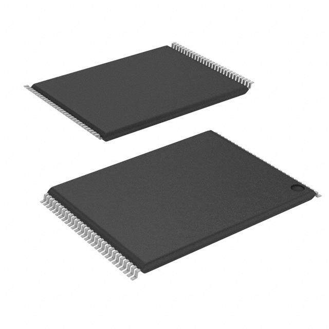
| 供应商器件封装 | 16-SOIC |
| 包装 | 管件 |
| 安装类型 | 表面贴装 |
| 封装/外壳 | 16-SOIC(0.154",3.90mm 宽) |
| 工作温度 | -40°C ~ 125°C |
| 延迟时间 | 90ns |
| 标准包装 | 45 |
| 电压-电源 | 10 V ~ 20 V |
| 电流-峰值 | 500mA |
| 输入类型 | 非反相 |
| 输出数 | 2 |
| 配置 | 高端 |
| 配置数 | 2 |
| 高压侧电压-最大值(自举) | 600V |


PDF Datasheet 数据手册内容提取
Datasheet No – PD97383 March 17, 2009 IRS21962S Dual channel high-side drivers with floating input Features Product Summary • Two independent high side output channels V 600 V • CMOS Schmitt trigger inputs with pull down resistor OFFSET • 5V compatible logic level inputs V 10 V – 20 V OUT • Immune to –Vs spike and tolerant to dVs/dt and I & I (typical) 0.5 A dVss/dt o+ o- • Typical operating frequency 200kHz t & t (typical) 90 ns • RoHS compliant ON OFF Package Type 16-Lead SOIC (narrow body) Typical Connection Diagram www.irf.com © 2007 International Rectifier
IRS21962S Table of Contents Page Description 3 Qualification Information 4 Absolute Maximum Ratings 5 Recommended Operating Conditions 5 Static Electrical Characteristics 6 Dynamic Electrical Characteristics 6 Functional Block Diagram 7 Input/Output Pin Equivalent Circuit Diagram 9 Lead Definitions 10 Lead Assignments 10 Package Details 11 Tape and Reel Details 12 Part Marking Information 13 Ordering Information 14 www.irf.com © 2008 International Rectifier 2
IRS21962S Description The IRS21962 is a high voltage, high speed power MOSFET and IGBT driver with propagation delay matched output channels. Proprietary HVIC and latch immune CMOS technologies enable ruggedized monolithic construction. The floating logic input is compatible with standard 5 V CMOS or LSTTL logic and can be operated up to 600 volts above the COM ground. The output driver feature a 500 mA high pulse current buffer stage designed for minimum driver cross-conduction. The floating channel can be used to drive an N-channel power MOSFET or IGBT in the high side configuration, which operates up to 600 V above COM ground. www.irf.com © 2008 International Rectifier 3
IRS21962S Qualification Information† Industrial†† Comments: This family of ICs has passed JEDEC’s Qualification Level Industrial qualification. IR’s Consumer qualification level is granted by extension of the higher Industrial level. MSL2††† 260°C Moisture Sensitivity Level SOIC16N (per IPC/JEDEC J-STD-020) Class B Machine Model (per JEDEC standard JESD22-A115) ESD Class 2 Human Body Model (per EIA/JEDEC standard EIA/JESD22-A114) Class 1, Level A IC Latch-Up Test (per JESD78) RoHS Compliant Yes † Qualification standards can be found at International Rectifier’s web site http://www.irf.com/ †† Higher qualification ratings may be available should the user have such requirements. Please contact your International Rectifier sales representative for further information. ††† Higher MSL ratings may be available for the specific package types listed here. Please contact your International Rectifier sales representative for further information. www.irf.com © 2008 International Rectifier 4
IRS21962S Absolute Maximum Ratings Absolute maximum ratings indicate sustained limits beyond which damage to the device may occur. All voltage parameters are absolute voltages referenced to COM, which is the –200V DC bus provided externally. Symbol Definition Min Max Units VCC Low side supply voltage -0.3 25 V VDD Input logic supply voltage -0.3 625 V VSS Input logic supply return VDD-25 VDD+0.3 V HIN1, HIN2 Input logic voltage VSS-0.3 VDD+0.3 V VB1, VB2 High side floating well positive supply voltage -0.3 625 V VS1 High side floating well negative supply voltage VB1-25 VB1+0.3 V VS2 High side floating well negative supply voltage VB2-25 VB2+0.3 V HO1 Floating gate drive output voltage VS1-0.3 VB1+0.3 V HO2 Floating gate drive output voltage VS2-0.3 VB2+0.3 V Allowable VS1 or VS2 offset supply transient relative to dVS/dt - 50 V/ns COM dVSS/dt Allowable VSS input supply transient relative to COM - 50 V/ns P Package Power Dissipation @ T <=+25°C - 1 W D A RθJA Thermal Resistance, Junction to Ambient - 100 °C/W T Junction Temperature -55 150 °C J T Storage Temperature -55 150 °C S T Lead temperature (Soldering, 10 seconds) - 300 °C L Recommended Operating Conditions For proper operation, the device should be used within the recommended conditions. All voltage parameters are absolute voltages referenced to COM, which is the –200V DC bus provided externally. The offset rating are tested with supplies of (VDD-VSS)=5V and (VCC-COM)=(VB1-VS1)= (VB2-VS2)=15V. Symbol Definition Min Max Units VCC Low side supply voltage 10 20 V VDD Input logic supply voltage VSS+4.5 VSS+5.5 V VSS Input logic supply offset voltage -0.3 600 V HIN1, HIN2 IN1~IN2 input voltage VSS VDD V VB1 High side floating well positive supply voltage VS1+10 VS1+20 V VB2 High side floating well positive supply voltage VS2+10 VS2+20 V VS1, VS2 High side floating well negative supply voltage -5 600 V HO1 Floating gate drive output voltage VS1 VB1 V HO2 Floating gate drive output voltage VS2 VB2 V T Ambient Temperature -40 125 °C A www.irf.com © 2008 International Rectifier 5
IRS21962S Static Electrical Characteristics (VDD-VSS)=5V and (VCC-COM)=(VBn-VSn)=15V. TA = 25°C. The parameters VIN,th+, VIN,th-, IIN+, IIN- , VDDUV+, and VDDUV- are referenced to VSS. The VBSUV+, VBSUV-, VOH, VOL, IO+, and IO- parameters are referenced to VS1 or VS2. The VCCUV+, VCCUV- parameters are referenced to COM. Test Symbol Definition Min Typ Max Units Conditions VDDUV+ VDD supply undervoltage positive going threshold 4.0 V VSS -COM = 5V VDDUV- VDD supply undervoltage negative going threshold 3.9 V VSS -COM = 5V VDDUVH VDD supply undervoltage lockout hysteresis 0.1 V VSS -COM = 5V V V supply undervoltage positive going threshold 7.5 8.6 9.7 V CCUV+ CC V V supply undervoltage negative going threshold 7.1 8.2 9.3 V CCUV- CC V V supply undervoltage lockout hysteresis --- 0.4 --- V CCUVH CC V V supply undervoltage positive going threshold 7.5 8.3 9.4 V BSUV+ BS V V supply undervoltage negative going threshold 6.9 7.7 8.8 V BSUV- BS V V supply undervoltage lockout hysteresis --- 0.6 --- V BSUVH BS ILKDD Input Logic offset supply leakage current --- --- 50 VDD = VSS = 600V ILKBS Highside floating well offset supply leakage current --- --- 50 µA VB = VS = 600V IQDD Quiescent VDD supply current --- 105 180 VIN = 0V or 5V IQBS Quiescent VBS supply current --- 100 175 VIN = 0V or 5V IQCC Quiescent VCC supply current --- 180 280 uA VIN = 0V or 5V V Logic “1” input threshold 3.5 IN,th+ VIN,th- Logic “0” input threshold 0.6 V VOH High level output voltage, VO -VBIAS --- --- 1 Io+=20mA VOL Low level output voltage, VO --- --- 1 V Io-=20mA IIN+ Logic “1” input bias current --- 5 --- VIN=5V IIN- Logic “0” input bias current --- 0 --- uA VIN=0V VO=15V, VIN=5V, IO+ Output high short circuit pulsed current --- 500 --- mA PW<=10us VO=0V,VIN=0VP, IO- Output low short circuit pulsed current --- 500 --- mA W<=10us Dynamic Electrical Characteristics (VDD-VSS)=5V and (VCC-COM)=(VBn-VSn)=15V. TA = 25. °C CL = 1000pF unless otherwise specified. All parameters are reference to COM. Symbol Definition Min Typ Max Unit Test Conditions t , t Propagation delay from input pin HIN to output on off 55 90 125 ns Vss=200V, Vs=0V pin HO tr Turn-on 10%-to-90% rise time at HO pin 25 70 ns Vss=200V, Vs=0V tf Turn-off 90%-to-10% fall time at HO pin 25 70 ns Vss=200V, Vs=0V www.irf.com © 2008 International Rectifier 6
IRS21962S Figure 1 Functional Block Diagram www.irf.com © 2008 International Rectifier 7
IRS21962S PWin 50% Input HIN 50% t ton tr off tf PWout 90% 90% Output HO 10% 10% Figure 2 Switching Time Waveforms HIN1 and HIN2 of 50% 50% Part A and Part B t tonA offA tf HO1 or HO2 90% 90% of Part A 10% 10% t t offB onB 90% HO1 or HO2 90% of Part B 10% 10% Figure 3 Switching Time Waveforms – Part to Part Propagation Delay Matching www.irf.com © 2008 International Rectifier 8
IRS21962S Input/Output Pin Equivalent Circuit Diagrams VB1 ESD Diode HO1 ESD RESD Diode VS1 VB2 ESD Diode HO2 ESD RESD Diode VS2 VB1 600V VB2 600V VDD 600V COM www.irf.com © 2008 International Rectifier 9
IRS21962S Lead Definitions: Pin Symbol Description 1 VDD Input logic supply voltage 2 HIN1 Logic input channel 1 3 HIN2 Logic input channel 2 4 VSS Input logic offset voltage 5 NC No connection 6 NC No connection 7 VCC Low side supply voltage 8 COM Ground 9 VS1 High side floating well offset voltage 10 HO1 Floating gate driver output voltage channel 1 11 VB1 High side floating well positive supply 12 NC No connection 13 NC No connection 14 VS2 High side floating well offset voltage 15 HO2 Floating gate driver output voltage channel 2 16 VB2 High side floating well positive supply Lead Assignments www.irf.com © 2008 International Rectifier 10
IRS21962S Package Details: SOIC16N www.irf.com © 2008 International Rectifier 11
IRS21962S Tape and Reel Details: SOIC16N LOADED TAPE FEE D DIRECTION B AA H D F C NOTE : CONTROLLING DIMENSION IN MM E G CARRIER TAPE DIMENSION FOR 16SOICN Metric Imperial Code Min Max Min Max A 7.90 8.10 0.311 0.318 B 3.90 4.10 0.153 0.161 C 15.70 16.30 0.618 0.641 D 7.40 7.60 0.291 0.299 E 6.40 6.60 0.252 0.260 F 10.20 10.40 0.402 0.409 G 1.50 n/a 0.059 n/a H 1.50 1.60 0.059 0.062 F D B C A E G H REEL DIMENSIONS FOR 16SOICN Metric Imperial Code Min Max Min Max A 329.60 330.25 12.976 13.001 B 20.95 21.45 0.824 0.844 C 12.80 13.20 0.503 0.519 D 1.95 2.45 0.767 0.096 E 98.00 102.00 3.858 4.015 F n/a 22.40 n/a 0.881 G 18.50 21.10 0.728 0.830 H 16.40 18.40 0.645 0.724 www.irf.com © 2008 International Rectifier 12
IRS21962S Part Marking Information Part number IRSxxxxx Date code YWW ? IR logo Pin 1 ? XXXX Lot Code Identifier (Prod mode – 4 digit SPN code) ? MARKING CODE P Lead Free Released Assembly site code Non-Lead Free Released Per SCOP 200-002 www.irf.com © 2008 International Rectifier 13
IRS21962S Ordering Information Standard Pack Base Part Number Package Type Complete Part Number Form Quantity Tube/Bulk 45 IRS21962SPBF IRS21962 SOIC16N Tape and Reel 2500 IRS21962STRPBF The information provided in this document is believed to be accurate and reliable. However, International Rectifier assumes no responsibility for the consequences of the use of this information. International Rectifier assumes no responsibility for any infringement of patents or of other rights of third parties which may result from the use of this information. No license is granted by implication or otherwise under any patent or patent rights of International Rectifier. The specifications mentioned in this document are subject to change without notice. This document supersedes and replaces all information previously supplied. For technical support, please contact IR’s Technical Assistance Center http://www.irf.com/technical-info/ WORLD HEADQUARTERS: 233 Kansas St., El Segundo, California 90245 Tel: (310) 252-7105 www.irf.com © 2008 International Rectifier 14