ICGOO在线商城 > IR3507ZMTRPBF
 Datasheet下载
- 型号: IR3507ZMTRPBF
- 制造商: International Rectifier
- 库位|库存: xxxx|xxxx
- 要求:
| 数量阶梯 | 香港交货 | 国内含税 |
| +xxxx | $xxxx | ¥xxxx |
查看当月历史价格
查看今年历史价格
IR3507ZMTRPBF产品简介:
ICGOO电子元器件商城为您提供IR3507ZMTRPBF由International Rectifier设计生产,在icgoo商城现货销售,并且可以通过原厂、代理商等渠道进行代购。 提供IR3507ZMTRPBF价格参考以及International RectifierIR3507ZMTRPBF封装/规格参数等产品信息。 你可以下载IR3507ZMTRPBF参考资料、Datasheet数据手册功能说明书, 资料中有IR3507ZMTRPBF详细功能的应用电路图电压和使用方法及教程。
| 参数 | 数值 |
| 产品目录 | 集成电路 (IC) |
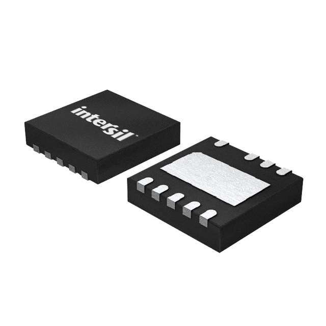
| 描述 | IC CTRL XPHASE3 20-MLPQ |
| 产品分类 | |
| 品牌 | International Rectifier |
| 数据手册 | |
| 产品图片 | |
| 产品型号 | IR3507ZMTRPBF |
| PCN组件/产地 | |
| rohs | 无铅 / 符合限制有害物质指令(RoHS)规范要求 |
| 产品系列 | XPhase3™ |
| 产品培训模块 | http://www.digikey.cn/PTM/IndividualPTM.page?site=cn&lang=zhs&ptm=26250 |
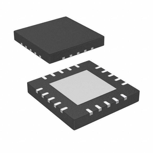
| 供应商器件封装 | 20-MLPQ(4x4) |
| 其它名称 | IR3507ZMTRPBFCT |
| 包装 | 剪切带 (CT) |
| 安装类型 | 表面贴装 |
| 封装/外壳 | 20-MLPQ |
| 工作温度 | 0°C ~ 125°C |
| 应用 | 处理器 |
| 标准包装 | 1 |
| 电压-电源 | 8 V ~ 28 V |
| 电流-电源 | 4mA |


PDF Datasheet 数据手册内容提取
IR3507Z DATA SHEET XPHASE3TM PHASE IC DESCRIPTION The IR3507Z Phase IC combined with an IR XPhase3TM Control IC provides a full featured and flexible way to implement power solutions for the latest high performance CPUs and ASICs. The “Control” IC provides overall system control and interfaces with any number of “Phase” ICs which each drive and monitor a single phase of a multiphase converter. The XPhase3TM architecture results in a power supply that is smaller, less expensive, and easier to design while providing higher efficiency than conventional approaches. FEATURES IR3507Z PHASE IC • Power State Indicator (PSI) interface provides the capability to maximize the efficiency at light loads. • 7V/2A gate drivers (4A GATEL sink current) • Converter output voltage up to 5.1 V (Limited to VCCL-1.4V) • Loss-less inductor current sensing • Feed-forward voltage mode control • Integrated boot-strap synchronous PFET • Only four external components per phase • 3 wire analog bus connects Control and Phase ICs (VID, Error Amp, IOUT) • 3 wire digital bus for accurate daisy-chain phase timing control without external components • Anti-bias circuitry prevents excessive sag in output voltage during PSI de-assertion • PSI input is ignored during power up • Debugging function isolates phase IC from the converter • Self-calibration of PWM ramp, current sense amplifier, and current share amplifier • Single-wire bidirectional average current sharing • Small thermally enhanced 20L 4 X 4mm MLPQ package • RoHS compliant APPLICATION CIRCUIT Figure 1 Application Circuit Page 1 of 19 IR Confidential April 2, 2009
IR3507Z ORDERING INFORMATION Part Number Package Order Quantity IR3507ZMTRPBF 20 Lead MLPQ 3000 per reel (4 x 4 mm body) * IR3507ZMPBF 20 Lead MLPQ 100 piece strips (4 x 4 mm body) * Samples only ABSOLUTE MAXIMUM RATINGS Stresses beyond those listed under “Absolute Maximum Ratings” may cause permanent damage to the device. These are stress ratings only and functional operation of the device at these or any other conditions beyond those indicated in the operational sections of the specifications are not implied. Operating Junction Temperature…………….. 0 to 150oC Storage Temperature Range………………….-65oC to 150oC ESD Rating………………………………………HBM Class 1C JEDEC Standard MSL Rating………………………………………2 Reflow Temperature…………………………….260oC PIN # PIN NAME V V I I MAX MIN SOURCE SINK 1 IOUT 8V -0.3V 1mA 1mA 2 PSI 8V -0.3V 1mA 1mA 3 DACIN 3.3V -0.3V 1mA 1mA 4 LGND n/a n/a n/a n/a 5 PHSIN 8V -0.3V 1mA 1mA 6 NC n/a n/a n/a n/a 7 PHSOUT 8V -0.3V 2mA 2mA 8 CLKIN 8V -0.3V 1mA 1mA 9 PGND 0.3V -0.3V 5A for 100ns, n/a 200mA DC 10 GATEL 8V -0.3V DC, -5V for 5A for 100ns, 5A for 100ns, 100ns 200mA DC 200mA DC 11 NC n/a n/a n/a n/a 12 VCCL 8V -0.3V n/a 5A for 100ns, 200mA DC 13 BOOST 40V -0.3V 1A for 100ns, 3A for 100ns, 100mA DC 100mA DC 14 GATEH 40V -0.3V DC, -5V for 3A for 100ns, 3A for 100ns, 100ns 100mA DC 100mA DC 15 SW 34V -0.3V DC, -5V for 3A for 100ns, n/a 100ns 100mA DC 16 VCC 34V -0.3V n/a 10mA 17 CSIN+ 8V -0.3V 1mA 1mA 18 CSIN- 8V -0.3V 1mA 1mA 19 EAIN 8V -0.3V 1mA 1mA 20 NC n/a n/a n/a n/a Note: 1. Maximum GATEH – SW = 8V 2. Maximum BOOST – GATEH = 8V Page 2 of 19 IR Confidential April 2, 2009
IR3507Z RECOMMENDED OPERATING CONDITIONS FOR RELIABLE OPERATION WITH MARGIN 8.0V ≤ VCC ≤ 28V, 4.75V ≤ VCCL ≤ 7.5V, 0 oC ≤ TJ ≤ 125 oC. 0.5V ≤ V(DACIN) ≤ 1.6V, 500kHz ≤ CLKIN ≤ 9MHz, 250kHz ≤ PHSIN ≤1.5MHz ELECTRICAL CHARACTERISTICS The electrical characteristics involve the spread of values guaranteed within the recommended operating conditions. Typical values represent the median values, which are related to 25°C. C = 3.3nF, C = 6.8nF (unless otherwise specified). GATEH GATEL PARAMETER TEST CONDITION MIN TYP MAX UNIT Gate Drivers GATEH Source Resistance BOOST – SW = 7V. Note 1 1.0 2.5 Ω GATEH Sink Resistance BOOST – SW = 7V. Note 1 1.0 2.5 Ω GATEL Source Resistance VCCL – PGND = 7V. Note 1 1.0 2.5 Ω GATEL Sink Resistance VCCL – PGND = 7V. Note 1 0.4 1.0 Ω GATEH Source Current BOOST=7V, GATEH=2.5V, SW=0V. 2.0 A GATEH Sink Current BOOST=7V, GATEH=2.5V, SW=0V. 2.0 A GATEL Source Current VCCL=7V, GATEL=2.5V, PGND=0V. 2.0 A GATEL Sink Current VCCL=7V, GATEL=2.5V, PGND=0V. 4.0 A GATEH Rise Time BOOST – SW = 7V, measure 1V to 4V 5 10 ns transition time GATEH Fall Time BOOST – SW = 7V, measure 4V to 1V 5 10 ns transition time GATEL Rise Time VCCL – PGND = 7V, Measure 1V to 4V 10 20 ns transition time GATEL Fall Time VCCL – PGND = 7V, Measure 4V to 1V 5 10 ns transition time GATEL low to GATEH high BOOST = VCCL = 7V, SW = PGND = 0V, 10 20 40 ns delay measure time from GATEL falling to 1V to GATEH rising to 1V GATEH low to GATEL high BOOST = VCCL = 7V, SW = PGND = 0V, 10 20 40 ns delay measure time from GATEH falling to 1V to GATEL rising to 1V Disable Pull-Down Note 1 30 80 130 kΩ Resistance Clock CLKIN Threshold Compare to V(VCCL) 40 45 57 % CLKIN Bias Current CLKIN = V(VCCL) -0.5 0.0 0.5 µA CLKIN Phase Delay Measure time from CLKIN<1V to GATEH>1V 40 75 125 ns PHSIN Threshold Compare to V(VCCL) 35 50 55 % PHSOUT Propagation Measure time from CLKIN > (VCCL * 50% ) 4 15 35 ns Delay to PHSOUT > (VCCL *50%), 10pF Load @125oC PHSIN Pull-Down 30 100 170 kΩ Resistance PHSOUT High Voltage I(PHSOUT) = -10mA, measure VCCL – 1 0.6 V PHSOUT PHSOUT Low Voltage I(PHSOUT) = 10mA 0.4 1 V Page 3 of 19 IR Confidential April 2, 2009
IR3507Z PARAMETER TEST CONDITION MIN TYP MAX UNIT PWM Comparator PWM Ramp Slope Vin=12V 42 52.5 57 mV/ %DC Input Offset Voltage Note 1 -5 0 5 mV EAIN Bias Current 0 ≤ EAIN ≤ 3V -5 -0.3 5 µA Minimum Pulse Width Note 1 55 70 ns Minimum GATEH Turn-off 20 80 160 ns Time Current Sense Amplifier CSIN+/- Bias Current -200 0 200 nA CSIN+/- Bias Current Note 1 -50 0 50 nA Mismatch Input Offset Voltage CSIN+ = CSIN- = DACIN. Measure -1 0 1 mV input referred offset from DACIN Gain 0.5V ≤ V(DACIN) < 1.6V 30.0 32.5 35.0 V/V Unity Gain Bandwidth C(IOUT)=10pF. Measure at IOUT. 4.8 6.8 8.8 MHz Note 1 Slew Rate 6 V/µs Differential Input Range 0.8V ≤ V(DACIN) ≤ 1.6V, Note 1 -10 50 mV Differential Input Range 0.5V ≤ V(DACIN) < 0.8V, Note 1 -5 50 mV Common Mode Input Range Note 1 0 Note2 V Rout at T = 25 oC Note 1 2.3 3.0 3.7 kΩ J Rout at T = 125 oC 3.6 4.7 5.4 kΩ J IOUT Source Current 0.5 1.6 2.9 mA IOUT Sink Current 0.5 1.4 2.9 mA Share Adjust Amplifier Input Offset Voltage Note 1 -3 0 3 mV Differential Input Range Note 1 -1 1 V Gain CSIN+ = CSIN- = DACIN. Note 1 4 5.0 6 V/V Unity Gain Bandwidth Note 1 4 8.5 17 kHz PWM Ramp Floor Voltage IOUT Open, Measure relative to DACIN -116 0 116 mV Maximum PWM Ramp Floor IOUT = DACIN – 200mV. Measure 120 180 240 mV Voltage relative to floor voltage. Minimum PWM Ramp Floor IOUT = DACIN + 200mV. Measure -220 -160 -100 mV Voltage relative to floor voltage. PSI Comparator Rising Threshold Voltage Note 1 520 620 700 mV Falling Threshold Voltage Note 1 400 550 650 mV Hysteresis Note 1 50 70 120 mV Resistance 200 500 850 kΩ Floating Voltage 800 1150 mV Page 4 of 19 IR Confidential April 2, 2009
IR3507Z PARAMETER TEST CONDITION MIN TYP MAX UNIT Body Brake Comparator Threshold Voltage with EAIN Measure relative to Floor Voltage -300 -200 -110 mV decreasing Threshold Voltage with EAIN Measure relative to Floor Voltage -200 -100 -10 mV increasing Hysteresis 70 105 130 mV Propagation Delay VCCL = 5V. Measure time from EAIN < 40 65 90 ns V(DACIN) (200mV overdrive) to GATEL transition to < 4V. OVP Comparator OVP Threshold Step V(IOUT) up until GATEL drives -1.0 -0.8 -0.4 V high. Compare to V(VCCL) Propagation Delay V(VCCL)=5V, Step V(IOUT) up from 15 40 70 ns V(DACIN) to V(VCCL). Measure time to V(GATEL)>4V. Synchronous Rectification Disable Comparator Threshold Voltage The ratio of V(CSIN-) / V(DACIN), below 66 75 86 % which V(GATEL) is always low. Negative Current Comparator Input Offset Voltage Note 1 -16 0 16 mV Propagation Delay Time Apply step voltage to V(CSIN+) – 100 200 400 ns V(CSIN-). Measure time to V(GATEL)< 1V. Bootstrap Diode Forward Voltage I(BOOST) = 30mA, VCCL = 6.8V 360 520 960 mV Debug Comparator Threshold Voltage Compare to V(VCCL) -250 -150 -50 mV General VCC Supply Current 8V ≤ V(VCC) < 10V 1.1 4.0 6.1 mA VCC Supply Current 10V ≤ V(VCC) ≤ 16V 1.1 2.0 4 mA VCCL Supply Current 3.1 8.0 12.1 mA BOOST Supply Current 4.75V ≤ V(BOOST)-V(SW )≤ 8V 0.5 1.5 3 mA DACIN Bias Current -1.5 -0.75 1 µA SW Floating Voltage 0.1 0.3 0.4 V Note 1: Guaranteed by design, but not tested in production Note 2: V -0.5V or V – 2.5V, whichever is lower CCL CC Page 5 of 19 IR Confidential April 2, 2009
IR3507Z PIN DESCRIPTION PIN# PIN SYMBOL PIN DESCRIPTION 1 IOUT Output of the Current Sense Amplifier is connected to this pin through a 3kΩ resistor. Voltage on this pin is equal to V(DACIN) + 33 [V(CSIN+) – V(CSIN-)]. Connecting all IOUT pins together creates a share bus which provides an indication of the average current being supplied by all the phases. The signal is used by the Control IC for voltage positioning and over-current protection. OVP mode is initiated if the voltage on this pin rises above V(VCCL)- 0.8V. 2 PSI Logic low is an active low (IE low=low power state). 3 DACIN Reference voltage input from the Control IC. The Current Sense signal and PWM ramp is referenced to the voltage on this pin. 4 LGND Ground for internal IC circuits. IC substrate is connected to this pin. 5 PHSIN Phase clock input. 6 NC N/A 7 PHSOUT Phase clock output. 8 CLKIN Clock input. 9 PGND Return for low side driver and reference for GATEH non-overlap comparator. 10 GATEL Low-side driver output and input to GATEH non-overlap comparator. 11 NC N/A 12 VCCL Supply for low-side driver. Internal bootstrap synchronous PFET is connected from this pin to the BOOST pin. 13 BOOST Supply for high-side driver. Internal bootstrap synchronous PFET is connected between this pin and the VCCL pin. 14 GATEH High-side driver output and input to GATEL non-overlap comparator. 15 SW Return for high-side driver and reference for GATEL non-overlap comparator. 16 VCC Supply for internal IC circuits. 17 CSIN+ Non-Inverting input to the current sense amplifier, and input to debug comparator. 18 CSIN- Inverting input to the current sense amplifier, and input to synchronous rectification disable comparator. 19 EAIN PWM comparator input from the error amplifier output of Control IC. Body Braking mode is initiated if the voltage on this pin is less than V(DACIN). 20 NC N/A Page 6 of 19 IR Confidential April 2, 2009
IR3507Z SYSTEM THEORY OF OPERATION System Description The system consists of one control IC and a scalable array of phase converters, each requiring one phase IC. The control IC communicates with the phase ICs using three digital buses, i.e., CLOCK, PHSIN, PHSOUT and three analog buses, i.e., DAC, EA, IOUT. The digital buses are responsible for switching frequency determination and accurate phase timing control without any external component. The analog buses are used for PWM control and current sharing among interleaved phases. The control IC incorporates all the system functions, i.e., VID, CLOCK signals, error amplifier, fault protections, current monitor, etc. The Phase IC implements the functions required by the converter of each phase, i.e., the gate drivers, PWM comparator and latch, over-voltage protection, phase disable circuit, current sensing and sharing, etc. PWM Control Method The PWM block diagram of the XPhase3TM architecture is shown in Figure 1. Feed-forward voltage mode control with trailing edge modulation is used. A high-gain wide-bandwidth voltage type error amplifier in the Control IC is used for the voltage control loop. Input voltage is sensed by the phase ICs and feed-forward control is realized. The feed-forward control compensates the ramp slope based on the change in input voltage. The input voltage can change due to variations in the silver box output voltage or due to the wire and PCB-trace voltage drop related to changes in load current. GATE DRIVE VOLTAGE VIN CONTROL IC PHSOUT PHASE IC VCC CLOCK GENERATOR CLKOUT CLKIN CLKQ VCCH D PHSOUT PHSIN 1 2 DROEMISENTANT GATEH CBST VOSNS+ VID6 PHSIN EAIN PCWOMMPARATOR+- PWMCD LLKRADQQTFCFRHH OFF VSCWCL COUT GVONDUT RAEMMPOLTIEF ISEERNSE + ENABLVEID6+ BBORDAYKING VID6 GPGATNEDL VOSNS- - VO RDAIMSPCHARG-E COMPARATOR OFF CLAMP +- VDAC PSI PSI LGND SHARE ADJUST ERROR AMPLIFIER + - +- VDAC EAOUT IOUT 3K +- -+VVIIDD66 CSAUEMRNPRSLEEINFTIER CSIN+ EARMRPOLRIFIER RCOMP RFB1 RFB VVIIDD66+ +- CCSRCS + CSIN- FB CCOMP CFB DACIN RVSETPT RDRP1 PHSOUT IROSC VSETPT RDRP PHASE IC IVSETPT CDRP IMON CLKIN CLKQ VCC VDAC D VCCH PHSIN 1 2 DROEMISENTAUN2T48 GATEH VADMRPP+- C o mTpheenrsmaatlion VVNDRPRTHRM EAIN PCWOMMPARATOR+- PWMCD LLKRADQQTFCFRHH OFVFID6 SVWCCL CBST IIN ENABLE VID6+ BODY GATEL RDAIMSPCHARG-E BCROAMKPIANRGATOR VID6 PGND CLAMP OFF +- PSI SHARE ADJUST PSI ERROR AMPLIFIER + CURRENT ISHARE 3K - -+VVIIDD66 SAEMNPSLEIFIER CSIN+ VID6 VID6++ +- CCSRCS DACIN CSIN- Figure 1: PWM Block Diagram Page 7 of 19 IR Confidential April 2, 2009
IR3507Z Frequency and Phase Timing Control The oscillator is located in the Control IC and the system clock frequency is programmable from 250kHz to 9MHZ by an external resistor. The control IC system clock signal (CLKOUT) is connected to CLKIN of all the phase ICs. The phase timing of the phase ICs is controlled by the daisy chain loop, where control IC phase clock output (PHSOUT) is connected to the phase clock input (PHSIN) of the first phase IC, and PHSOUT of the first phase IC is connected to PHSIN of the second phase IC, etc. and PHSOUT of the last phase IC is connected back to PHSIN of the control IC. During power up, the control IC sends out clock signals from both CLKOUT and PHSOUT pins and detects the feedback at PHSIN pin to determine the phase number and monitor any fault in the daisy chain loop. Figure 2 shows the phase timing for a four phase converter. The switching frequency is set by the resistor ROSC. The clock frequency equals the number of phase times the switching frequency. Control IC CLKOUT (Phase IC CLKIN) Control IC PHSOUT (Phase IC1 PHSIN) Phase IC1 PWM Latch SET Phase IC 1 PHSOUT (Phase IC2 PHSIN) Phase IC 2 PHSOUT (Phase IC3 PHSIN) Phase IC 3 PHSOUT (Phase IC4 PHSIN) Phase IC4 PHSOUT (Control IC PHSIN) Figure 2: Four Phase Oscillator Waveforms PWM Operation The PWM comparator is located in the phase IC. Upon receiving the falling edge of a clock pulse, the PWM latch is set; the PWMRMP voltage begins to increase; the low side driver is turned off, and the high side driver is then turned on after the non-overlap time. When the PWMRMP voltage exceeds the error amplifier’s output voltage, the PWM latch is reset. This turns off the high side driver and then turns on the low side driver after the non-overlap time; it activates the ramp discharge clamp, which quickly discharges the PWMRMP capacitor to the output voltage of share adjust amplifier in phase IC until the next clock pulse. The PWM latch is reset dominant allowing all phases to go to zero duty cycle within a few tens of nanoseconds in response to a load step decrease. Phases can overlap and go up to 100% duty cycle in response to a load step increase with turn-on gated by the clock pulses. An error amplifier output voltage greater than the common mode input range of the PWM comparator results in 100% duty cycle regardless of the voltage of the PWM ramp. This arrangement guarantees the error amplifier is always in control and can demand 0 to 100% duty cycle as required. It also favors response to a load step decrease, which is appropriate given the low output to input voltage ratio of most systems. The inductor current will increase much more rapidly than decrease in response to load transients. The error amplifier is a high speed amplifier with 110 dB of open loop gain. It is not unity gain stable. This control method is designed to provide “single cycle transient response” where the inductor current changes in response to load transients within a single switching cycle maximizing the effectiveness of the power train and minimizing the output capacitor requirements. Page 8 of 19 IR Confidential April 2, 2009
IR3507Z An additional advantage of the architecture is that differences in ground or input voltage at the phases have no effect on operation since the PWM ramps are referenced to VDAC. Figure 3 depicts PWM operating waveforms under various conditions. PHASE IC CLOCK PULSE EAIN PWMRMP VDAC GATEH GATEL STEADY-STATE DUTY CYCLE INCREASE DUTY CYCLE DECREASE DUTY CYCLE DECREASE DUE TO LOAD STEADY-STATE OPERATION DUE TO LOAD DUE TO VIN INCREASE DECREASE (BODY BRAKING) OR FAULT OPERATION INCREASE (FEED-FORWARD) (VCCLUV, OCP, VID=11111X) Figure 3: PWM Operating Waveforms Body BrakingTM In a conventional synchronous buck converter, the minimum time required to reduce the current in the inductor in response to a load step decrease is; L*(I −I ) T = MAX MIN SLEW V O The slew rate of the inductor current can be significantly increased by turning off the synchronous rectifier in response to a load step decrease. The switch node voltage is then forced to decrease until conduction of the synchronous rectifier’s body diode occurs. This increases the voltage across the inductor from Vout to Vout + V . The BODYDIODE minimum time required to reduce the current in the inductor in response to a load transient decrease is now; L*(I −I ) T = MAX MIN SLEW V +V O BODYDIODE Since the voltage drop in the body diode is often comparable to the output voltage, the inductor current slew rate can be increased significantly. This patented technique is referred to as “body braking” and is accomplished through the “body braking comparator” located in the phase IC. If the error amplifier’s output voltage drops below the output voltage of the share adjust amplifier in the phase IC, this comparator turns off the low side gate driver. Lossless Average Inductor Current Sensing Inductor current can be sensed by connecting a series resistor and a capacitor network in parallel with the inductor and measuring the voltage across the capacitor, as shown in Figure 4. The equation of the sensing network is, 1 R +sL v (s)=v (s) =i (s) L C L L 1+sR C 1+sR C CS CS CS CS Page 9 of 19 IR Confidential April 2, 2009
IR3507Z Usually the resistor Rcs and capacitor Ccs are chosen so that the time constant of Rcs and Ccs equals the time constant of the inductor which is the inductance L over the inductor DCR (RL). If the two time constants match, the voltage across Ccs is proportional to the current through L, and the sense circuit can be treated as if only a sense resistor with the value of RL was used. The mismatch of the time constants does not affect the measurement of inductor DC current, but affects the AC component of the inductor current. vL L RL iL VO RCS CCS CO Current vCcS Sense Amp CSOUT Figure 4: Inductor Current Sensing and Current Sense Amplifier The advantage of sensing the inductor current versus high side or low side sensing is that actual output current being delivered to the load is obtained rather than peak or sampled information about the switch currents. The output voltage can be positioned to meet a load line based on real time information. Except for a sense resistor in series with the inductor, this is the only sense method that can support a single cycle transient response. Other methods provide no information during either load increase (low side sensing) or load decrease (high side sensing). An additional problem associated with peak or valley current mode control for voltage positioning is that they suffer from peak-to-average errors. These errors will show in many ways but one example is the effect of frequency variation. If the frequency of a particular unit is 10% low, the peak to peak inductor current will be 10% larger and the output impedance of the converter will drop by about 10%. Variations in inductance, current sense amplifier bandwidth, PWM prop delay, any added slope compensation, input voltage, and output voltage are all additional sources of peak-to-average errors. Current Sense Amplifier A high speed differential current sense amplifier is located in the phase IC, as shown in Figure 4. Its gain is nominally 32.5, and the 3850 ppm/ºC increase in inductor DCR should be compensated in the voltage loop feedback path. The current sense amplifier can accept positive differential input up to 50mV and negative up to -10mV before clipping. The output of the current sense amplifier is summed with the DAC voltage and sent to the control IC and other phases through an on-chip 3KΩ resistor connected to the IOUT pin. The IOUT pins of all the phases are tied together and the voltage on the share bus represents the average current through all the inductors and is used by the control IC for voltage positioning and current limit protection. The input offset of this amplifier is calibrated to +/- 1mV in order to reduce the current sense error. The input offset voltage is the primary source of error for the current share loop. In order to achieve very small input offset error and superior current sharing performance, the current sense amplifier continuously calibrates itself. This calibration algorithm creates ripple on IOUT bus with a frequency of f /(32*28) in a multiphase architecture. sw Average Current Share Loop Current sharing between phases of the converter is achieved by the average current share loop in each phase IC. The output of the current sense amplifier is compared with the average current at the share bus. If current in a phase is smaller than the average current, the share adjust amplifier of the phase will pull down the starting point of the PWM ramp thereby increasing its duty cycle and output current; if current in a phase is larger than the average current, the share adjust amplifier of the phase will pull up the starting point of the PWM ramp thereby decreasing its duty cycle and output current. The current share amplifier is internally compensated so that the crossover frequency of the current Page 10 of 19 IR Confidential April 2, 2009
IR3507Z share loop is much slower than that of the voltage loop and the two loops do not interact. For proper current sharing the output of current sense amplifier should note exceed (VCCL-1.4V) under all operating condition. IR3507Z THEORY OF OPERATION Block Diagram The Block diagram of the IR3507Z is shown in Figure 5, and specific features are discussed in the following sections. CLKIN CLKQ PHSOUT D GATEH DRIVER Q_100%DUTY RMPOUT - PWM LATCH + 200mV PHESAININ EAIPNWM COM-PARATOR PWM_CLKDSQ PWMQ BGOAOTESHT CLKQ 1LP0AW0TM%CQ HDDU+TY .. RDEOSM.EITNANT R GOLAVATETERCHLH ANPON- GOCAVOTEMERPHLA ARNPAOTNO-R SW PWM_CLK Q_100%DUTY . CLKQ Q S - VCCL RMPOUT PWM RESET SET R + PHSIN PWM RAMP GATDEOLMI NNANOTN- GATEL NON1-V VCC VCC GENERATOR Q D OVERLAP OVERLAP CALIBRATION CLK LATCH COMPARATOR DACIN-SHARE_ADJ R 1V Q S ANTI-BIAS + BCOODMYP ABRRAATKOIRNG LATCH SDOEMTINARNT - - EAIN GATEL 100mV + NEGATIVE DRIVER VCCL DACIN+ 200mVOVP CURRENT GATEL LATCH SHARE_A-DJ VCCL COMPARATOR PGND - DEBUG OFF 0.8V + RESET Q RS SYNCHRONOUS RECTIFICATION 0.15V (LOW=OPEN) DOMINANT DISABLE COMPARATOR + IOUT SAHDAJRUEST NCEOGMAPTAIRVAET OCRURRENT +- CAUMRPRLEINFTI ESRENSE DEBUG - AMPLIFI+ER 3K +- +CSAOUT X32.5+- COMPARATOR CCSSIINN-+ - DACIN CALIBRATION IROSCDACIN + X0.75 CALIBRATION LGND PSI ASSERT 1V PSI Q D VCCL 8QCLKD VICRCOLSC COMPARATOR 500K PHSIN - PSI RCLK CRLK (CLKIN IF 1-PHASE) + 620mV 550mV Figure 5: Block diagram Tri-State Gate Drivers The gate drivers can deliver up to 2A peak current (4A sink current for bottom driver). An adaptive non-overlap circuit monitors the voltage on the GATEH and GATEL pins to prevent MOSFET shoot-through current while minimizing body diode conduction. The non-overlap latch is added to eliminate the error triggering caused by the switching noise. An enable signal is provided by the control IC to the phase IC without the addition of a dedicated signal line. The error amplifier output of the control IC drives low in response to any fault condition such as VCCL under voltage or output overload. The IR3507Z Body BrakingTM comparator detects this and drives bottom gate output low. This tri-state operation prevents negative inductor current and negative output voltage during power- down. Page 11 of 19 IR Confidential April 2, 2009
IR3507Z A synchronous rectification disable comparator is used to detect converter CSIN- pin voltage, which represents local converter output voltage. If the voltage is below 75% of VDAC and negative current is detected, GATEL drives low, which disables synchronous rectification and eliminates negative current during power-up. The gate drivers pull low if the supply voltages are below the normal operating range. An 80kΩ resistor is connected across the GATEH/GATEL and PGND pins to prevent the GATEH/GATEL voltage from rising due to leakage or other causes under these conditions. PWM Ramp Every time the phase IC is powered up PWM ramp magnitude is calibrated to generate a 52.5 mV/% ramp for a VCC=12V. For example, for a 15 % duty ratio the ramp amplitude is 750mV for VCC=12V. Feed-forward control is achieved by varying the PWM ramp proportionally with VCC voltage after calibration. In response to a load step-up the error amplifier can demand 100 % duty cycle. In order to avoid pulse skipping under this scenario and allow the BOOST cap to replenish, a minimum off time is allowed in this mode of operation. As shown in Figure 6, 100 % duty is detected by comparing the PWM latch output (PWMQ) and its input clock (PWM_CLK). If the PWMQ is high when the PWM_CLK is asserted the TopFET turnoff is initiated. The TopFET is again turned on once the RMPOUT drops within 200 mV of the VDAC. NORMAL OPERATION 100 % DUTY OPERATION CLKIN PHSIN (2 Phase Design) EAIN RMPOUT VDAC+200mV VDAC PWMQ 80ns Figure 6: PWM Operation during normal and 100 % duty mode. Power State Indicator (PSI) function From a system perspective, the PSI input is controlled by the system and is forced low when the load current is lower than a preset limit and forced high when load current is higher than the preset limit. IR3507Z can accept an active low signal on its PSI input and force the drivers into tri-state, effectively forcing the phase IC into off state. As shown in Figure 7, once the PSI assert signal is received the IC waits for eight PHSIN pulses before forcing the drivers into tri-state. This delay is required to prevent the IC from responding to any high frequency PSI input. The de-assertion of the PSI input is succeeded by an increase in the load current. In order to prevent excess discharging of the output capacitors and reduction in the circulating sinking current between phases, the IC makes sure that the topFET is turned on first during de-assertion. This is achieved with the help of an Anti-Bias TM circuitry. Irrespective of the PSI input, the IOUT bus remains connected to current share bus of the system. The PSI circuit is disabled during power up while the output voltage is below 0.75*VDAC. The maximum PSI de-assert delay is determined by the CLKIN period. Page 12 of 19 IR Confidential April 2, 2009
IR3507Z PSI ASSERT PSI DE-ASSERT PHSIN PSI ANTI-BIAS LATCH ENSURES GATEH GATEH TURNS ON FIRST GATEL Figure 7: PSI assertion and De-assertion Debugging Mode If CSIN+ pin is pulled up to VCCL voltage, IR3507Z enters into debugging mode. Both drivers are pulled low and IOUT output is disconnected from the current share bus, which isolates this phase IC from other phases. However, the phase timing from PHSIN to PHSOUT does not change. Emulated Bootstrap Diode IR3507Z integrates a PFET to emulate the bootstrap diode. If two or more top MOSFETs are to be driven at higher switching frequency, an external bootstrap diode connected from VCCL pin to BOOST pin may be needed. OUTPUT OVP VOLTAGE THRESHOLD 130mV (VO) VCCL-800 mV IOUT(ISHARE) GATEH (PHASE IC) GATEL (PHASE IC) FAULT LATCH ERROR AMPLIFIER OUTPUT VDAC (EAOUT) AFTER NORMAL OPERATION OVP CONDITION OVP Figure 8: Over-voltage protection waveforms Page 13 of 19 IR Confidential April 2, 2009
IR3507Z Over Voltage Protection (OVP) The IR3507Z includes over-voltage protection that turns on the low side MOSFET to protect the load in the event of a shorted high-side MOSFET, converter out of regulation, or connection of the converter output to an excessive output voltage. As shown in Figure 6, if IOUT pin voltage is above V(VCCL) – 0.8V, which represents over-voltage condition detected by control IC, the over-voltage latch is set. GATEL drives high and GATEH drives low. The OVP circuit overrides the normal PWM operation and within approximately 150ns will fully turn-on the low side MOSFET, which remains ON until IOUT drops below V(VCCL) – 0.8V when over voltage ends. The over voltage fault is latched in control IC and can only be reset by cycling the power to control IC. The error amplifier output (EAIN) is pulled down by control IC and will remain low. The lower MOSFETs alone can not clamp the output voltage however an SCR or N-MOSFET could be triggered with the OVP output to prevent processor damage. Operation at Higher Output Voltage The proper operation of the phase IC is ensured for output voltage up to 5.1V. Similarly, the minimum VCC for proper operation of the phase IC is 8 V. Below this voltage, the current sharing performance of the phase IC is affected. DESIGN PROCEDURES - IR3507Z Inductor Current Sensing Capacitor CCS and Resistor RCS The DC resistance of the inductor is utilized to sense the inductor current. Usually the resistor RCS and capacitor CCS in parallel with the inductor are chosen to match the time constant of the inductor, and therefore the voltage across the capacitor CCS represents the inductor current. If the two time constants are not the same, the AC component of the capacitor voltage is different from that of the real inductor current. The time constant mismatch does not affect the average current sharing among the multiple phases, but does effect the current signal IOUT as well as the output voltage during the load current transient if adaptive voltage positioning is adopted. Measure the inductance L and the inductor DC resistance RL. Pre-select the capacitor CCS and calculate RCS as follows. L R R = L (1) CS C CS Bootstrap Capacitor CBST Depending on the duty cycle and gate drive current of the phase IC, a capacitor in the range of 0.1uF to 1uF is needed for the bootstrap circuit. Decoupling Capacitors for Phase IC A 0.1uF-1uF decoupling capacitor is required at the VCCL pin. CURRENT SHARE LOOP COMPENSATION The internal compensation of current share loop ensures that crossover frequency of the current share loop is at least one decade lower than that of the voltage loop so that the interaction between the two loops is eliminated. The crossover frequency of current share loop is approximately 8 kHz. Page 14 of 19 IR Confidential April 2, 2009
IR3507Z LAYOUT GUIDELINES The following layout guidelines are recommended to reduce the parasitic inductance and resistance of the PCB layout; therefore, minimizing the noise coupled to the IC. • Dedicate at least one middle layer for a ground plane. • Separate analog bus (EAIN, DACIN, and IOUT) from digital bus (CLKIN, PSI, PHSIN, and PHSOUT) to reduce the noise coupling. • Connect PGND to LGND pins of each phase IC to the ground tab, which is tied to PGND planes respectively through vias. • Place current sense resistors and capacitors (RCS and CCS) close to phase IC. Use Kelvin connection for the inductor current sense wires, but separate the two wires by ground polygon or as differential routing. The wire from the inductor terminal to CSIN- should not cross over the fast transition nodes, i.e., switching nodes, gate drive outputs, and bootstrap nodes. • Place the decoupling capacitors CVCC and CVCCL as close as possible to VCC and VCCL pins of the phase IC respectively. • Place the phase IC as close as possible to the MOSFETs to reduce the parasitic resistance and inductance of the gate drive paths. • Place the input ceramic capacitors close to the drain of top MOSFET and the source of bottom MOSFET. Use combination of different packages of ceramic capacitors. • There are two switching power loops. One loop includes the input capacitors, top MOSFET, inductor, output capacitors and the load; another loop consists of bottom MOSFET, inductor, output capacitors and the load. Route the switching power paths using wide and short traces or polygons; use multiple vias for connections between layers. Page 15 of 19 IR Confidential April 2, 2009
IR3507Z PCB Metal and Component Placement • Lead land width should be equal to nominal part lead width. The minimum lead to lead spacing should be ≥ 0.2mm to minimize shorting. • Lead land length should be equal to maximum part lead length + 0.3 mm outboard extension + 0.05mm inboard extension. The outboard extension ensures a large and inspectable toe fillet, and the inboard extension will accommodate any part misalignment and ensure a fillet. • Center pad land length and width should be equal to maximum part pad length and width. However, the minimum metal to metal spacing should be ≥ 0.17mm for 2 oz. Copper (≥ 0.1mm for 1 oz. Copper and ≥ 0.23mm for 3 oz. Copper) • Four 0.3mm diameter vias shall be placed in the pad land spaced at 1.2mm, and connected to ground to minimize the noise effect on the IC and to transfer heat to the PCB. • No PCB traces should be routed nor vias placed under any of the 4 corners of the IC package. Doing so can cause the IC to rise up from the PCB resulting in poor solder joints to the IC leads. Page 16 of 19 IR Confidential April 2, 2009
IR3507Z Solder Resist • The solder resist should be pulled away from the metal lead lands and center pad by a minimum of 0.06mm. The solder resist mis-alignment is a maximum of 0.05mm and it is recommended that the lead lands are all Non Solder Mask Defined (NSMD). Therefore, pulling the S/R 0.06mm will always ensure NSMD pads. • The minimum solder resist width is 0.13mm. At the inside corner of the solder resist where the lead land groups meet, it is recommended to provide a fillet so a solder resist width of ≥ 0.17mm remains. • Ensure that the solder resist in-between the lead lands and the pad land is ≥ 0.15mm due to the high aspect ratio of the solder resist strip separating the lead lands from the pad land. • The 4 vias in the land pad should be tented with solder resist 0.4mm diameter, or 0.1mm larger than the diameter of the via. Page 17 of 19 IR Confidential April 2, 2009
IR3507Z Stencil Design • The stencil apertures for the lead lands should be approximately 80% of the area of the lead lands. Reducing the amount of solder deposited will minimize the occurrence of lead shorts. Since for 0.5mm pitch devices the leads are only 0.25mm wide, the stencil apertures should not be made narrower; openings in stencils < 0.25mm wide are difficult to maintain repeatable solder release. • The stencil lead land apertures should therefore be shortened in length by 80% and centered on the lead land. • The land pad aperture should be striped with 0.25mm wide openings and spaces to deposit approximately 50% area of solder on the center pad. If too much solder is deposited on the center pad the part will float and the lead lands will be open. • The maximum length and width of the land pad stencil aperture should be equal to the solder resist opening minus an annular 0.2mm pull back to decrease the incidence of shorting the center land to the lead lands when the part is pushed into the solder paste. Page 18 of 19 IR Confidential April 2, 2009
IR3507Z PACKAGE INFORMATION 20L MLPQ (4 x 4 mm Body) – θ = 32oC/W, θ = 3oC/W JA JC Data and specifications subject to change without notice. This product has been designed and qualified for the Consumer market. Qualification Standards can be found on IR’s Web site. IR WORLD HEADQUARTERS: 233 Kansas St., El Segundo, California 90245, USA Tel: (310) 252-7105 TAC Fax: (310) 252-7903 Visit us at www.irf.com for sales contact information. Page 19 of 19 IR Confidential April 2, 2009