ICGOO在线商城 > 滤波器 > EMI/RFI 滤波器(LC,RC 网络) > IP4256CZ5-W,115
 Datasheet下载
- 型号: IP4256CZ5-W,115
- 制造商: NXP Semiconductors
- 库位|库存: xxxx|xxxx
- 要求:
| 数量阶梯 | 香港交货 | 国内含税 |
| +xxxx | $xxxx | ¥xxxx |
查看当月历史价格
查看今年历史价格
IP4256CZ5-W,115产品简介:
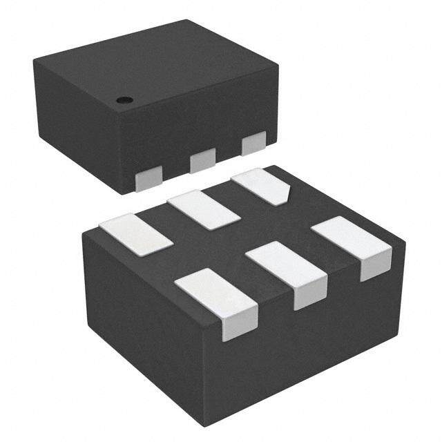
ICGOO电子元器件商城为您提供IP4256CZ5-W,115由NXP Semiconductors设计生产,在icgoo商城现货销售,并且可以通过原厂、代理商等渠道进行代购。 IP4256CZ5-W,115价格参考¥询价-¥询价。NXP SemiconductorsIP4256CZ5-W,115封装/规格:EMI/RFI 滤波器(LC,RC 网络), RC (Pi) EMI Filter 2nd Order Low Pass 2 Channel R = 100 Ohms, C = 19pF (Total) SOT-665。您可以下载IP4256CZ5-W,115参考资料、Datasheet数据手册功能说明书,资料中有IP4256CZ5-W,115 详细功能的应用电路图电压和使用方法及教程。
Nexperia USA Inc.的型号IP4256CZ5-W,115是一款EMI/RFI滤波器,属于LC/RC网络器件,主要用于抑制电磁干扰(EMI)和射频干扰(RFI)。该器件常用于提高电子设备的电磁兼容性(EMC),确保设备在复杂的电磁环境中正常工作,同时不对外界产生过多干扰。

主要应用场景包括:

1. 消费类电子产品:如智能手机、平板电脑、笔记本电脑等便携设备,用于保护USB、HDMI、DisplayPort等高速接口免受高频干扰影响,提升信号完整性。

2. 通信设备:用于有线或无线通信模块中,防止射频干扰对数据传输造成影响,确保通信质量稳定。

3. 工业控制系统:在工业自动化设备中,用于保护敏感的控制电路免受电机、变频器等高噪声设备的干扰。

4. 汽车电子系统:应用于车载娱乐系统、摄像头模块、传感器接口等,满足汽车电磁环境对高可靠性的要求。

5. 电源管理电路:用于电源输入端口,滤除来自电源线的传导干扰,提高系统稳定性。

该器件采用小型封装(如DFN),适合高密度PCB布局,具备良好的高频性能和可靠性,适用于需要高性能滤波和空间受限的设计场景。
| 参数 | 数值 |
| 产品目录 | |
| 描述 | IC EMI FILTER ESD 2CH SOT665ESD 抑制器 2CH IC EMI FILTER ESD |
| ESD保护 | 是 |
| 产品分类 | EMI/RFI 滤波器(LC、RC 网络)ESD 抑制器 |
| 品牌 | NXP Semiconductors |
| 产品手册 | |
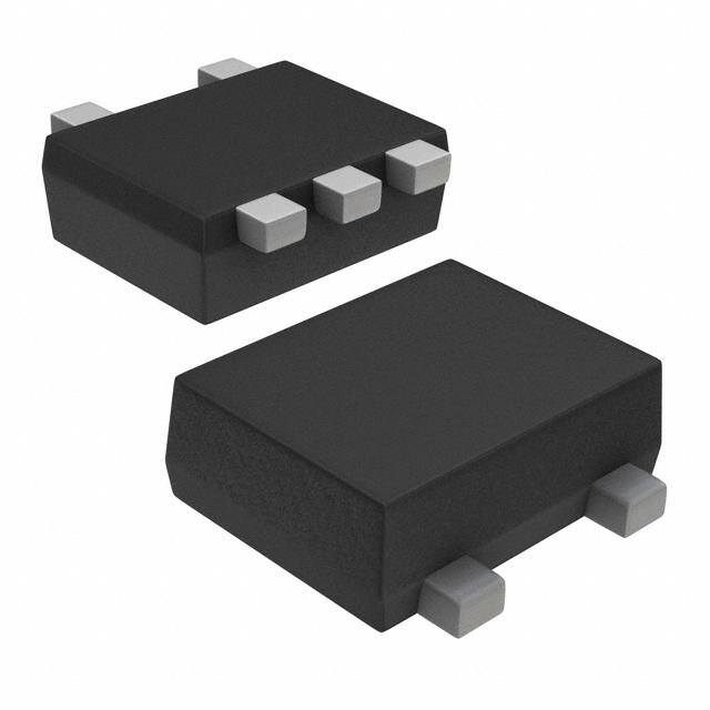
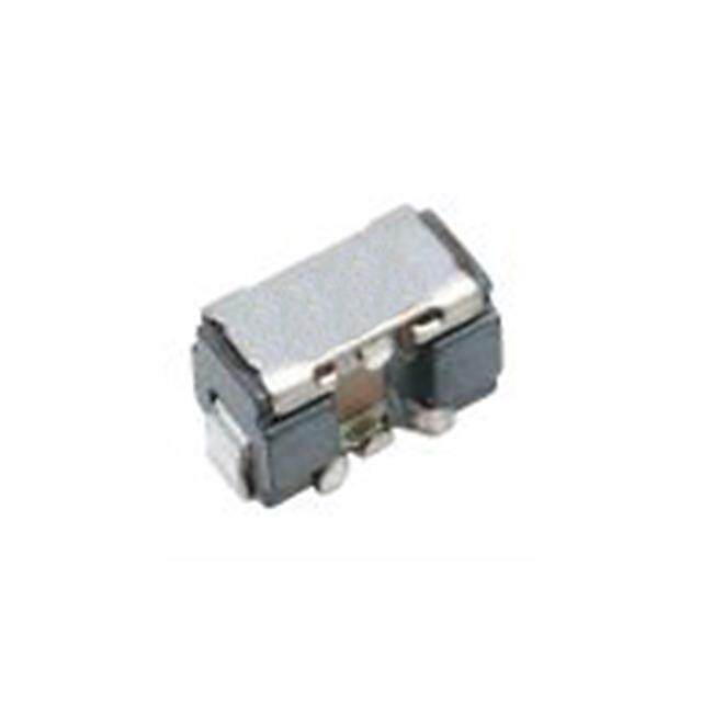
| 产品图片 |
|
| rohs | 符合RoHS无铅 / 符合限制有害物质指令(RoHS)规范要求 |
| 产品系列 | NXP Semiconductors IP4256CZ5-W,115- |
| 数据手册 | |
| 产品型号 | IP4256CZ5-W,115 |
| PCN封装 | |
| PCN设计/规格 | |
| 中心/截止频率 | - |
| 产品种类 | ESD 抑制器 |
| 其它名称 | 568-5871-6 |
| 击穿电压 | 6.8 V |
| 包装 | Digi-Reel® |
| 商标 | NXP Semiconductors |
| 大小/尺寸 | 0.063" 长 x 0.047" 宽(1.60mm x 1.20mm) |
| 封装 | Reel |
| 封装/外壳 | SOT-665 |
| 封装/箱体 | SOT-665 |
| 工作温度 | -40°C ~ 85°C |
| 工厂包装数量 | 4000 |
| 应用 | 移动设备的数据线路 |
| 应用说明 | |
| 技术 | RC(Pi) |
| 数值 | R = 100 欧姆,C = 30pF(总计) |
| 标准包装 | 1 |
| 滤波器阶数 | 2nd |
| 电容 | 30 pF |
| 电流 | - |
| 电阻-通道(Ω) | 100 |
| 端接类型 | Solder Pad |
| 类型 | 低通 |
| 衰减值 | 25dB @ 800MHz ~ 3GHz |
| 通道数 | 2 |
| 高度 | 0.024"(0.60mm) |


- 商务部:美国ITC正式对集成电路等产品启动337调查
- 曝三星4nm工艺存在良率问题 高通将骁龙8 Gen1或转产台积电
- 太阳诱电将投资9.5亿元在常州建新厂生产MLCC 预计2023年完工
- 英特尔发布欧洲新工厂建设计划 深化IDM 2.0 战略
- 台积电先进制程称霸业界 有大客户加持明年业绩稳了
- 达到5530亿美元!SIA预计今年全球半导体销售额将创下新高
- 英特尔拟将自动驾驶子公司Mobileye上市 估值或超500亿美元
- 三星加码芯片和SET,合并消费电子和移动部门,撤换高东真等 CEO
- 三星电子宣布重大人事变动 还合并消费电子和移动部门
- 海关总署:前11个月进口集成电路产品价值2.52万亿元 增长14.8%


PDF Datasheet 数据手册内容提取
Important notice Dear Customer, On 7 February 2017 the former NXP Standard Product business became a new company with the tradename Nexperia. Nexperia is an industry leading supplier of Discrete, Logic and PowerMOS semiconductors with its focus on the automotive, industrial, computing, consumer and wearable application markets In data sheets and application notes which still contain NXP or Philips Semiconductors references, use the references to Nexperia, as shown below. Instead of http://www.nxp.com, http://www.philips.com/ or http://www.semiconductors.philips.com/, use http://www.nexperia.com Instead of sales.addresses@www.nxp.com or sales.addresses@www.semiconductors.philips.com, use salesaddresses@nexperia.com (email) Replace the copyright notice at the bottom of each page or elsewhere in the document, depending on the version, as shown below: - © NXP N.V. (year). All rights reserved or © Koninklijke Philips Electronics N.V. (year). All rights reserved Should be replaced with: - © Nexperia B.V. (year). All rights reserved. If you have any questions related to the data sheet, please contact our nearest sales office via e-mail or telephone (details via salesaddresses@nexperia.com). Thank you for your cooperation and understanding, Kind regards, Team Nexperia
IP4256CZ3-M/CZ5-W/CZ6-F Single and dual-channel passive filter network with ESD protection Rev. 1 — 23 July 2010 Product data sheet 1. Product profile 1.1 General description The IP4256CZ3-M is a single-channel low-pass filter while the IP4256CZ5-W and IP4256CZ6-F are dual-channel RC low-pass filters. All devices provide high-level ElectroStatic Discharge(ESD) protection. The devices are designed to protect a range of portable communication transmitter applications against unwanted RF signals. The devices incorporate diodes to provide protection to downstream components from ESDvoltages up to ±25kV contact discharge far exceeding IEC61000-4-2, level4. The devices are manufactured using monolithic silicon technology in lead-free plastic packages. 1.2 Features and benefits (cid:132) Pb-free, Restriction of Hazardous Substances(RoHS) compliant and free of halogen and antimony(Dark Green compliant) (cid:132) 100Ω series channel resistance and 30pF channel capacitance at 0V bias voltage(DC) (cid:132) ESDprotection up to ±25kV contact discharge far exceeding IEC61000-4-2, level4 (cid:132) Single and dual-channel integrated π-type RC filter network (cid:132) IP4256CZ3-M: single-channel device in a 3-pin Quad Flat-pack No-leads(QFN) compatible MicroPak plastic package (cid:132) IP4256CZ5-W: dual-channel device in a 5-pin plastic package with 0.5mm pitch (cid:132) IP4256CZ6-F: dual-channel device in a 6-pin QFN compatible MicroPak plastic package with 0.5mm pitch 1.3 Applications (cid:132) General-purpose ElectroMagnetic Interference(EMI), Radio Frequency Interference(RFI) filtering and downstream ESD protection for: (cid:139)Cellular phone and Personal Communication System(PCS) mobile handset (cid:139)Cordless telephone (cid:139)Wireless data (WAN/LAN) system
IP4256CZ3-M/CZ5-W/CZ6-F NXP Semiconductors Single and dual-channel passive filter network with ESD protection 1.4 Quick reference data Table 1. Quick reference data Symbol Parameter Conditions Min Typ Max Unit V electrostatic all pins to ground [1] ESD discharge voltage contact discharge - - ±25 kV air discharge - - ±25 kV R channel series 80 100 120 Ω s(ch) resistance C channel capacitance for the total channel; ch f=100kHz V =0V - 30 - pF bias(DC) V =2.5V - 19 - pF bias(DC) [1] According to IEC61000-4-2 model. 2. Pinning information Table 2. Pinning Pin Description Simplified outline Graphic symbol IP4256CZ3-M(SOT883) 1 and 2 channel 1 filter 3 ground(GND) 1 Rs(ch) 3 1 2 2 Cch Cch 2 2 Transparent top view 3 018aaa042 IP4256CZ5-W(SOT665) 1 and 5 channel 1 filter 5 4 Rs(ch) 2 ground(GND) 1,3 4,5 3 and 4 channel 2 filter Cch Cch 2 2 2 1 2 3 018aaa043 IP4256CZ6-F(SOT886) 1 and 6 channel 1 filter 1 2 3 Rs(ch) 2 and 5 ground(GND) 1,3 4,6 3 and 4 channel 2 filter Cch Cch 2 2 2,5 6 5 4 018aaa044 bottom view IP4256CZ3-M_CZ5-W_CZ6-F All information provided in this document is subject to legal disclaimers. © NXP B.V. 2010. All rights reserved. Product data sheet Rev. 1 — 23 July 2010 2 of 13
IP4256CZ3-M/CZ5-W/CZ6-F NXP Semiconductors Single and dual-channel passive filter network with ESD protection 3. Ordering information Table 3. Ordering information Type number Package Name Description Version IP4256CZ3-M SC-101 leadless ultra small plastic package; 3solder lands; SOT883 body1.0×0.6×0.5 mm IP4256CZ5-W - plastic surface-mounted package; 5leads SOT665 IP4256CZ6-F XSON-6 plastic extremely thin small outline package; no leads; SOT886 6terminals; body1×1.45×0.5mm 4. Marking Table 4. Marking codes Type number Marking code IP4256CZ3-M 6M IP4256CZ5-W 6W IP4256CZ6-F 6F 5. Limiting values Table 5. Limiting values In accordance with the Absolute Maximum Rating System (IEC 60134). Symbol Parameter Conditions Min Max Unit V supply voltage −0.5 +5.6 V CC V electrostatic discharge all pins to ground [1] ESD voltage contact discharge - ±25 kV air discharge - ±25 kV IEC 61000-4-2, level4 [2] contact discharge - ±8 kV air discharge - ±15 kV P channel power dissipation T =85°C - 60 mW ch amb P total power dissipation T =85°C - 120 mW tot amb T storage temperature −55 +150 °C stg T ambient temperature −40 +85 °C amb [1] According to IEC61000-4-2 model. [2] Devices withstand up to 1000 discharges of ±25kV according to the IEC61000-4-2 model without degradation and exceeds the specified level4 (8kV contact discharge). IP4256CZ3-M_CZ5-W_CZ6-F All information provided in this document is subject to legal disclaimers. © NXP B.V. 2010. All rights reserved. Product data sheet Rev. 1 — 23 July 2010 3 of 13
IP4256CZ3-M/CZ5-W/CZ6-F NXP Semiconductors Single and dual-channel passive filter network with ESD protection 6. Characteristics Table 6. Channel characteristics T =25°C unless otherwise specified. amb Symbol Parameter Conditions Min Typ Max Unit R channel series resistance 80 100 120 Ω s(ch) C channel capacitance for the total channel; ch f=100kHz V =0V - 30 - pF bias(DC) V =2.5V - 19 - pF bias(DC) I reverse leakage current per channel; V =3.5V - - 0.1 μA RM I V breakdown voltage positive clamp; I =1mA 5.8 - 9 V BR I V forward voltage negative clamp; I =1mA −1.5 - +0.4 V F F T able 7. Frequency characteristics T =25°C unless otherwise specified. amb Symbol Parameter Conditions Min Typ Max Unit α insertion loss R =50Ω; R =50Ω il source L 800MHz<f <3GHz 20 - - dB i f =1GHz - 25 - dB i α crosstalk attenuation R =50Ω; R =50Ω; - 25 - dB ct source L 800MHz<f <3GHz i IP4256CZ3-M_CZ5-W_CZ6-F All information provided in this document is subject to legal disclaimers. © NXP B.V. 2010. All rights reserved. Product data sheet Rev. 1 — 23 July 2010 4 of 13
IP4256CZ3-M/CZ5-W/CZ6-F NXP Semiconductors Single and dual-channel passive filter network with ESD protection 7. Application information 7.1 Insertion loss The devices are specifically designed as EMI/RFI filters for multichannel interfaces. The measured insertion loss in a 50Ω system is shown in Figure2. The insertion loss was measured using a test Printed-Circuit Board(PCB) utilizing laser-drilled micro-via holes that connect the PCB ground plane to the ground pins of the device. DUT IN OUT 50 Ω TEST BOARD 50 Ω Vgen 018aaa016 Fig 1. Frequency response setup 018aaa045 0 α il (dB) (1) (2) −20 (3) (4) (5) −40 −60 10−1 1 10 102 103 104 f (MHz) (1) IP4256CZ3-M (2) IP4256CZ5-W; pins1to5 (3) IP4256CZ5-W; pins3to4 (4) IP4256CZ6-F; pins1to6 (5) IP4256CZ6-F; pins3to4 Fig 2. Frequency response curves IP4256CZ3-M_CZ5-W_CZ6-F All information provided in this document is subject to legal disclaimers. © NXP B.V. 2010. All rights reserved. Product data sheet Rev. 1 — 23 July 2010 5 of 13
IP4256CZ3-M/CZ5-W/CZ6-F NXP Semiconductors Single and dual-channel passive filter network with ESD protection 7.2 Example applications The IP4256CZ3-M, IP4256CZ5-W and IP4256CZ6-F are designed as EMI/RFI filters for multichannel interfaces. Device selection must be made taking the following into account: • the maximum clock frequency • the driver strength and the capacitive load • the capacitive load of the heat sink • the maximum applicable rise and fall times 7.2.1 Medium-speed applications: LCD interfaces The devices can be used with digital interfaces running at clock speeds up to 25MHz. Typical applications include LCD interfaces. 7.2.2 Low-speed applications: keypads, serial and control interfaces The devices are ideally suited for applications with low transfer speeds which demand robust ESDprotection and strong EMIfiltering. This includes keypads, low-speed serial interfaces and low-speed control signals. The very small footprint of the devices makes it easy to locate the ESD and EMIprotection very close to the interface to be protected. IP4256CZ3-M_CZ5-W_CZ6-F All information provided in this document is subject to legal disclaimers. © NXP B.V. 2010. All rights reserved. Product data sheet Rev. 1 — 23 July 2010 6 of 13
IP4256CZ3-M/CZ5-W/CZ6-F NXP Semiconductors Single and dual-channel passive filter network with ESD protection 8. Package outline Leadless ultra small plastic package; 3 solder lands; body 1.0 x 0.6 x 0.5 mm SOT883 L L1 2 b 3 e b1 1 e1 A A1 E D 0 0.5 1 mm scale DIMENSIONS (mm are the original dimensions) UNIT A(1) mAa1x. b b1 D E e e1 L L1 0.50 0.20 0.55 0.62 1.02 0.30 0.30 mm 0.03 0.35 0.65 0.46 0.12 0.47 0.55 0.95 0.22 0.22 Note 1. Including plating thickness OUTLINE REFERENCES EUROPEAN ISSUE DATE VERSION IEC JEDEC JEITA PROJECTION 03-02-05 SOT883 SC-101 03-04-03 Fig 3. Package outline SOT883(SC-101) IP4256CZ3-M_CZ5-W_CZ6-F All information provided in this document is subject to legal disclaimers. © NXP B.V. 2010. All rights reserved. Product data sheet Rev. 1 — 23 July 2010 7 of 13
IP4256CZ3-M/CZ5-W/CZ6-F NXP Semiconductors Single and dual-channel passive filter network with ESD protection Plastic surface-mounted package; 5 leads SOT665 D A E X S Y S HE 5 4 A 1 2 3 c e1 bp w M A Lp e detail X 0 1 2 mm scale DIMENSIONS (mm are the original dimensions) UNIT A bp c D E e e1 HE Lp w y 0.6 0.27 0.18 1.7 1.3 1.7 0.3 mm 1.0 0.5 0.1 0.1 0.5 0.17 0.08 1.5 1.1 1.5 0.1 OUTLINE REFERENCES EUROPEAN ISSUE DATE VERSION IEC JEDEC JEITA PROJECTION 04-11-08 SOT665 06-03-16 Fig 4. Package outline SOT665 IP4256CZ3-M_CZ5-W_CZ6-F All information provided in this document is subject to legal disclaimers. © NXP B.V. 2010. All rights reserved. Product data sheet Rev. 1 — 23 July 2010 8 of 13
IP4256CZ3-M/CZ5-W/CZ6-F NXP Semiconductors Single and dual-channel passive filter network with ESD protection XSON6: plastic extremely thin small outline package; no leads; 6 terminals; body 1 x 1.45 x 0.5 mm SOT886 b 1 2 3 4× L1 L (2) e 6 5 4 e1 e1 6× A (2) A1 D E terminal 1 index area 0 1 2 mm scale DIMENSIONS (mm are the original dimensions) UNIT mA(a1x) mAa1x b D E e e1 L L1 0.25 1.5 1.05 0.35 0.40 mm 0.5 0.04 0.6 0.5 0.17 1.4 0.95 0.27 0.32 Notes 1. Including plating thickness. 2. Can be visible in some manufacturing processes. OUTLINE REFERENCES EUROPEAN ISSUE DATE VERSION IEC JEDEC JEITA PROJECTION 04-07-15 SOT886 MO-252 04-07-22 Fig 5. Package outline SOT886(XSON-6/MO-252) IP4256CZ3-M_CZ5-W_CZ6-F All information provided in this document is subject to legal disclaimers. © NXP B.V. 2010. All rights reserved. Product data sheet Rev. 1 — 23 July 2010 9 of 13
IP4256CZ3-M/CZ5-W/CZ6-F NXP Semiconductors Single and dual-channel passive filter network with ESD protection 9. Revision history Table 8. Revision history Document ID Release date Data sheet status Change notice Supersedes IP4256CZ3-M_CZ5-W_ 20100723 Product data sheet - - CZ6-Fv.1 IP4256CZ3-M_CZ5-W_CZ6-F All information provided in this document is subject to legal disclaimers. © NXP B.V. 2010. All rights reserved. Product data sheet Rev. 1 — 23 July 2010 10 of 13
IP4256CZ3-M/CZ5-W/CZ6-F NXP Semiconductors Single and dual-channel passive filter network with ESD protection 10. Legal information 10.1 Data sheet status Document status[1][2] Product status[3] Definition Objective [short] data sheet Development This document contains data from the objective specification for product development. Preliminary [short] data sheet Qualification This document contains data from the preliminary specification. Product [short] data sheet Production This document contains the product specification. [1] Please consult the most recently issued document before initiating or completing a design. [2] The term ‘short data sheet’ is explained in section “Definitions”. [3] The product status of device(s) described in this document may have changed since this document was published and may differ in case of multiple devices. The latest product status information is available on the Internet at URLhttp://www.nxp.com. 10.2 Definitions malfunction of an NXP Semiconductors product can reasonably be expected to result in personal injury, death or severe property or environmental damage. NXP Semiconductors accepts no liability for inclusion and/or use of Draft — The document is a draft version only. The content is still under NXP Semiconductors products in such equipment or applications and internal review and subject to formal approval, which may result in therefore such inclusion and/or use is at the customer’s own risk. modifications or additions. NXP Semiconductors does not give any representations or warranties as to the accuracy or completeness of Applications — Applications that are described herein for any of these information included herein and shall have no liability for the consequences of products are for illustrative purposes only. NXP Semiconductors makes no use of such information. representation or warranty that such applications will be suitable for the specified use without further testing or modification. Short data sheet — A short data sheet is an extract from a full data sheet with the same product type number(s) and title. A short data sheet is intended Customers are responsible for the design and operation of their applications for quick reference only and should not be relied upon to contain detailed and and products using NXP Semiconductors products, and NXP Semiconductors full information. For detailed and full information see the relevant full data accepts no liability for any assistance with applications or customer product sheet, which is available on request via the local NXP Semiconductors sales design. It is customer’s sole responsibility to determine whether the NXP office. In case of any inconsistency or conflict with the short data sheet, the Semiconductors product is suitable and fit for the customer’s applications and full data sheet shall prevail. products planned, as well as for the planned application and use of customer’s third party customer(s). Customers should provide appropriate Product specification — The information and data provided in a Product design and operating safeguards to minimize the risks associated with their data sheet shall define the specification of the product as agreed between applications and products. NXP Semiconductors and its customer, unless NXP Semiconductors and NXP Semiconductors does not accept any liability related to any default, customer have explicitly agreed otherwise in writing. In no event however, damage, costs or problem which is based on any weakness or default in the shall an agreement be valid in which the NXP Semiconductors product is customer’s applications or products, or the application or use by customer’s deemed to offer functions and qualities beyond those described in the third party customer(s). Customer is responsible for doing all necessary Product data sheet. testing for the customer’s applications and products using NXP Semiconductors products in order to avoid a default of the applications and 10.3 Disclaimers the products or of the application or use by customer’s third party customer(s). NXP does not accept any liability in this respect. Limited warranty and liability — Information in this document is believed to Limiting values — Stress above one or more limiting values (as defined in be accurate and reliable. However, NXP Semiconductors does not give any the Absolute Maximum Ratings System of IEC60134) will cause permanent representations or warranties, expressed or implied, as to the accuracy or damage to the device. Limiting values are stress ratings only and (proper) completeness of such information and shall have no liability for the operation of the device at these or any other conditions above those given in consequences of use of such information. the Recommended operating conditions section (if present) or the Characteristics sections of this document is not warranted. Constant or In no event shall NXP Semiconductors be liable for any indirect, incidental, repeated exposure to limiting values will permanently and irreversibly affect punitive, special or consequential damages (including - without limitation - lost the quality and reliability of the device. profits, lost savings, business interruption, costs related to the removal or replacement of any products or rework charges) whether or not such Terms and conditions of commercial sale — NXP Semiconductors damages are based on tort (including negligence), warranty, breach of products are sold subject to the general terms and conditions of commercial contract or any other legal theory. sale, as published at http://www.nxp.com/profile/terms, unless otherwise Notwithstanding any damages that customer might incur for any reason agreed in a valid written individual agreement. In case an individual whatsoever, NXP Semiconductors’ aggregate and cumulative liability towards agreement is concluded only the terms and conditions of the respective customer for the products described herein shall be limited in accordance agreement shall apply. NXP Semiconductors hereby expressly objects to with the Terms and conditions of commercial sale of NXP Semiconductors. applying the customer’s general terms and conditions with regard to the purchase of NXP Semiconductors products by customer. Right to make changes — NXP Semiconductors reserves the right to make changes to information published in this document, including without No offer to sell or license — Nothing in this document may be interpreted or limitation specifications and product descriptions, at any time and without construed as an offer to sell products that is open for acceptance or the grant, notice. This document supersedes and replaces all information supplied prior conveyance or implication of any license under any copyrights, patents or to the publication hereof. other industrial or intellectual property rights. Suitability for use — NXP Semiconductors products are not designed, Export control — This document as well as the item(s) described herein authorized or warranted to be suitable for use in life support, life-critical or may be subject to export control regulations. Export might require a prior safety-critical systems or equipment, nor in applications where failure or authorization from national authorities. IP4256CZ3-M_CZ5-W_CZ6-F All information provided in this document is subject to legal disclaimers. © NXP B.V. 2010. All rights reserved. Product data sheet Rev. 1 — 23 July 2010 11 of 13
IP4256CZ3-M/CZ5-W/CZ6-F NXP Semiconductors Single and dual-channel passive filter network with ESD protection Quick reference data — The Quick reference data is an extract of the product for such automotive applications, use and specifications, and (b) product data given in the Limiting values and Characteristics sections of this whenever customer uses the product for automotive applications beyond document, and as such is not complete, exhaustive or legally binding. NXP Semiconductors’ specifications such use shall be solely at customer’s own risk, and (c) customer fully indemnifies NXP Semiconductors for any Non-automotive qualified products — Unless this data sheet expressly liability, damages or failed product claims resulting from customer design and states that this specific NXP Semiconductors product is automotive qualified, use of the product for automotive applications beyond NXP Semiconductors’ the product is not suitable for automotive use. It is neither qualified nor tested standard warranty and NXP Semiconductors’ product specifications. in accordance with automotive testing or application requirements. NXP Semiconductors accepts no liability for inclusion and/or use of non-automotive qualified products in automotive equipment or applications. 10.4 Trademarks In the event that customer uses the product for design-in and use in automotive applications to automotive specifications and standards, customer Notice: All referenced brands, product names, service names and trademarks (a) shall use the product without NXP Semiconductors’ warranty of the are the property of their respective owners. 11. Contact information For more information, please visit: http://www.nxp.com For sales office addresses, please send an email to: salesaddresses@nxp.com IP4256CZ3-M_CZ5-W_CZ6-F All information provided in this document is subject to legal disclaimers. © NXP B.V. 2010. All rights reserved. Product data sheet Rev. 1 — 23 July 2010 12 of 13
IP4256CZ3-M/CZ5-W/CZ6-F NXP Semiconductors Single and dual-channel passive filter network with ESD protection 12. Contents 1 Product profile. . . . . . . . . . . . . . . . . . . . . . . . . . 1 1.1 General description . . . . . . . . . . . . . . . . . . . . . 1 1.2 Features and benefits. . . . . . . . . . . . . . . . . . . . 1 1.3 Applications . . . . . . . . . . . . . . . . . . . . . . . . . . . 1 1.4 Quick reference data . . . . . . . . . . . . . . . . . . . . 2 2 Pinning information. . . . . . . . . . . . . . . . . . . . . . 2 3 Ordering information. . . . . . . . . . . . . . . . . . . . . 3 4 Marking. . . . . . . . . . . . . . . . . . . . . . . . . . . . . . . . 3 5 Limiting values. . . . . . . . . . . . . . . . . . . . . . . . . . 3 6 Characteristics. . . . . . . . . . . . . . . . . . . . . . . . . . 4 7 Application information. . . . . . . . . . . . . . . . . . . 5 7.1 Insertion loss . . . . . . . . . . . . . . . . . . . . . . . . . . 5 7.2 Example applications . . . . . . . . . . . . . . . . . . . . 6 7.2.1 Medium-speed applications: LCD interfaces . . 6 7.2.2 Low-speed applications: keypads, serial and control interfaces . . . . . . . . . . . . . . . . . . . . . . . 6 8 Package outline. . . . . . . . . . . . . . . . . . . . . . . . . 7 9 Revision history. . . . . . . . . . . . . . . . . . . . . . . . 10 10 Legal information. . . . . . . . . . . . . . . . . . . . . . . 11 10.1 Data sheet status . . . . . . . . . . . . . . . . . . . . . . 11 10.2 Definitions. . . . . . . . . . . . . . . . . . . . . . . . . . . . 11 10.3 Disclaimers. . . . . . . . . . . . . . . . . . . . . . . . . . . 11 10.4 Trademarks. . . . . . . . . . . . . . . . . . . . . . . . . . . 12 11 Contact information. . . . . . . . . . . . . . . . . . . . . 12 12 Contents. . . . . . . . . . . . . . . . . . . . . . . . . . . . . . 13 Please be aware that important notices concerning this document and the product(s) described herein, have been included in section ‘Legal information’. © NXP B.V. 2010. All rights reserved. For more information, please visit: http://www.nxp.com For sales office addresses, please send an email to: salesaddresses@nxp.com Date of release: 23 July 2010 Document identifier: IP4256CZ3-M_CZ5-W_CZ6-F