ICGOO在线商城 > INA223AIDSKT
 Datasheet下载
- 型号: INA223AIDSKT
- 制造商: Texas Instruments
- 库位|库存: xxxx|xxxx
- 要求:
| 数量阶梯 | 香港交货 | 国内含税 |
| +xxxx | $xxxx | ¥xxxx |
查看当月历史价格
查看今年历史价格
INA223AIDSKT产品简介:
ICGOO电子元器件商城为您提供INA223AIDSKT由Texas Instruments设计生产,在icgoo商城现货销售,并且可以通过原厂、代理商等渠道进行代购。 提供INA223AIDSKT价格参考以及Texas InstrumentsINA223AIDSKT封装/规格参数等产品信息。 你可以下载INA223AIDSKT参考资料、Datasheet数据手册功能说明书, 资料中有INA223AIDSKT详细功能的应用电路图电压和使用方法及教程。
| 参数 | 数值 |
| 产品目录 | 集成电路 (IC)半导体 |
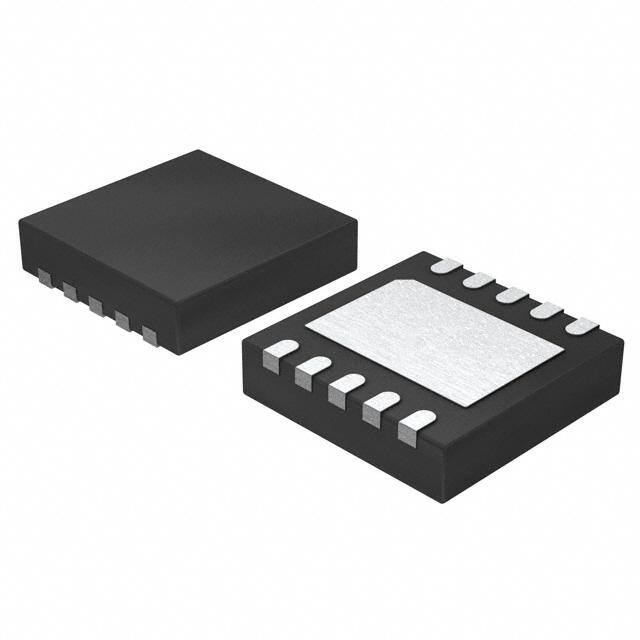
| 描述 | IC CURRENT SHUNT MONITOR 10SON电流灵敏放大器 Ana Out Crnt Shunt & Vltg Instant Pwr Mon |
| 产品分类 | |
| 品牌 | Texas Instruments |
| 产品手册 | |
| 产品图片 |
|
| rohs | 符合RoHS无铅 / 符合限制有害物质指令(RoHS)规范要求 |
| 产品系列 | 放大器 IC,电流灵敏放大器,Texas Instruments INA223AIDSKT零漂移 |
| 数据手册 | |
| 产品型号 | INA223AIDSKT |
| 产品种类 | 电流灵敏放大器 |
| 供应商器件封装 | 10-SON (2.5x2.5) |
| 共模抑制比—最小值 | 92 dB |
| 其它名称 | 296-30550-6 |
| 制造商产品页 | http://www.ti.com/general/docs/suppproductinfo.tsp?distId=10&orderablePartNumber=INA223AIDSKT |
| 功能 | 电流/电压监控器 |
| 包装 | Digi-Reel® |
| 商标 | Texas Instruments |
| 安装类型 | 表面贴装 |
| 安装风格 | SMD/SMT |
| 封装 | Reel |
| 封装/外壳 | 10-WFDFN 裸露焊盘 |
| 封装/箱体 | WSON-10 |
| 工作温度 | -40°C ~ 105°C |
| 工厂包装数量 | 250 |
| 感应方法 | 高/低端 |
| 拓扑结构 | Current Shunt Feedback |
| 最大工作温度 | + 105 C |
| 最小工作温度 | - 40 C |
| 标准包装 | 1 |
| 电压-输入 | 0 V ~ 26 V |
| 电流-输出 | - |
| 电源电压-最大 | 5.5 V |
| 电源电压-最小 | 2.7 V |
| 电源电流 | 250 uA |
| 精度 | - |
| 系列 | INA223 |
| 输出电压 | 1.5 V |


.jpg)


PDF Datasheet 数据手册内容提取
INA223 www.ti.com SBOS528–JUNE2012 Analog Output Current Shunt and Voltage Instantaneous Power Monitor CheckforSamples:INA223 FEATURES DESCRIPTION 1 • WideCommon-ModeRange:0Vto26V The INA223 is a voltage-output device that monitors 23 the current, bus voltage, and power of a supply line • ±100 µVOffset(Max,Gain=300V/V) bysensingavoltagedropacrossashuntatcommon- • Accuracy mode voltages from 0 V to 26 V. The common-mode – ±0.25%ShuntVoltageGainError(Max) voltage range is independent of the supply voltage. The low offset of the Zerø-Drift architecture enables – ±0.15%BusVoltageGainError(Max) current sensing with maximum drops across the – 1.25%PowerError(Max) shuntaslowas10mV,full-scale. – 0.3μV/°COffsetDrift(Max) The INA223 includes a two-wire interface used for – 50ppm/°CGainDrift(Max) adjusting the configuration settings of the device. The • ProgrammableGains interface is used to control the signal (current shunt voltage, bus voltage, or power) that is directed to the – CurrentShuntVoltageGains:20,128,300 device output. Multiple gain and attenuation settings – BusVoltageAttenuations:1/10,1/5,2/5 can be programmed through the two-wire interface to • Monitors/Measures/Reports: allow for application-specific configurations. The programmable gain feature also allows the device to – InstantaneousPower be operated over a much wider dynamic current load – BusVoltage range without having to switch the sensing element – LoadCurrent used. • QuiescentCurrent:250µA(Max) A shutdown feature is available to disable the device • ShutdownCurrent:1µA(Max) and effectively disconnect it from the shunt resistor and supply voltage, thus reducing the drain on the APPLICATIONS battery. • NotebookComputers The INA223 operates from a single +2.7-V to +5.5-V supply,drawingamaximumsupplycurrentof250µA. • CellPhones It is specified over the extended temperature range of • TelecomEquipment –40°C to +105°C, and is offered in an SON-10 • PowerManagement package. CBYPASS Power Supply RSHUNT 0.1mF (0V to 26V) Load VS(Supply Voltage) Attenuator RPULLUP 4.7kW VIN- VOUT SCL VIN+ Two-Wire SDA Interface A0 INA223 GND 1 Pleasebeawarethatanimportantnoticeconcerningavailability,standardwarranty,anduseincriticalapplicationsof TexasInstrumentssemiconductorproductsanddisclaimerstheretoappearsattheendofthisdatasheet. TransZorbisatrademarkofGeneralInstruments,Inc. 2 Allothertrademarksarethepropertyoftheirrespectiveowners. 3 PRODUCTIONDATAinformationiscurrentasofpublicationdate. Copyright©2012,TexasInstrumentsIncorporated Products conform to specifications per the terms of the Texas Instruments standard warranty. Production processing does not necessarilyincludetestingofallparameters.
INA223 SBOS528–JUNE2012 www.ti.com This integrated circuit can be damaged by ESD. Texas Instruments recommends that all integrated circuits be handled with appropriateprecautions.Failuretoobserveproperhandlingandinstallationprocedurescancausedamage. ESDdamagecanrangefromsubtleperformancedegradationtocompletedevicefailure.Precisionintegratedcircuitsmaybemore susceptibletodamagebecauseverysmallparametricchangescouldcausethedevicenottomeetitspublishedspecifications. PACKAGEINFORMATION(1) PACKAGE PACKAGE PRODUCT PACKAGE-LEAD DESIGNATOR MARKING INA223 SON-10 DSK P223 (1) Forthemostcurrentpackageandorderinginformation,seethePackageOptionAddendumlocatedattheendofthisdatasheet,orvisit thedeviceproductfolderatwww.ti.com. ABSOLUTE MAXIMUM RATINGS(1) Overoperatingfree-airtemperaturerange,unlessotherwisenoted. INA223 UNIT Supplyvoltage +6 V Analoginputs, Differential(VIN+)–(VIN–) –26to+26 V VIN+,VIN– (2) Common-mode(3) (GND–0.3)to+26 V Inputcurrentintoanypin(3) 5 mA Operatingtemperature –55to+150 °C Storagetemperature –65to+150 °C Junctiontemperature +150 °C Humanbodymodel(HBM) 2500 V Electrostatic discharge Charged-devicemodel(CDM) 1000 V (ESD)ratings Machinemodel(MM) 200 V (1) Stressesabovetheseratingsmaycausepermanentdamage.Exposuretoabsolutemaximumconditionsforextendedperiodsmay degradedevicereliability.Thesearestressratingsonly,andfunctionaloperationofthedeviceattheseoranyotherconditionsbeyond thosespecifiedisnotimplied. (2) V +andV –arethevoltagesatthe+INand–INpins,respectively. IN IN (3) Inputvoltageatanypinmayexceedthevoltageshownifthecurrentatthatpinislimitedto5mA. 2 SubmitDocumentationFeedback Copyright©2012,TexasInstrumentsIncorporated ProductFolderLink(s):INA223
INA223 www.ti.com SBOS528–JUNE2012 ELECTRICAL CHARACTERISTICS AtT =+25°C,V =(V +)–(V –)=10mV,V =3.3V,andV +=12V,unlessotherwisenoted. A SENSE IN IN S IN INA223 PARAMETER TESTCONDITIONS MIN TYP MAX UNIT INPUT VCM Common-modeinputrange TA=–40°Cto+105°C 0 26 V TA=–40°Cto+105°C,VIN+=0Vto+26V, 92 106 dB VSENSE=0mV,Currentshuntvoltagegain=20V/V CMR Common-moderejection TA=–40°Cto+105°C,VIN+=0Vto+26V, VSENSE=0mV,Currentshuntvoltagegain=128V/V, 100 120 dB 300V/V Currentshuntvoltagegain=20V/V ±75 ±300 μV VOS Shuntoffsetvoltage,RTI(1) Currentshuntvoltagegain=128V/V ±20 ±150 μV Currentshuntvoltagegain=300V/V ±15 ±100 μV TA=–40°Cto+105°C,currentshuntvoltagegain=20V/V 0.6 1 μV/°C dVOS/dT vstemperature TA=–40°Cto+105°C,currentshuntvoltagegain=128V/V, 0.1 0.3 300V/V VS=+2.7Vto+5.5V,currentshuntvoltagegain=20V/V ±15 ±50 μV/V PSR vspowersupply VS=+2.7Vto+5.5V,currentshuntvoltagegain=128V/V ±5 ±25 μV/V VS=+2.7Vto+5.5V,currentshuntvoltagegain=300V/V ±2.5 ±15 μV/V Busvoltagegain=0.1V/V ±2.5 ±20 mV VOS Busoffsetvoltage,RTI(1) Busvoltagegain=0.2V/V ±2.5 ±15 mV Busvoltagegain=0.4V/V ±1.5 ±10 mV TA=–40°Cto+105°C,busvoltagegain=0.1V/V 15 40 μV/°C dVOS/dT vstemperature TA=–40°Cto+105°C,busvoltagegain=0.2V/V,0.4V/V 10 30 μV/°C PSR vspowersupply VS=+2.7Vto+5.5V ±9 ±15 mV/V Enabled,VIN+,VIN– 15 18 25 μA IB Inputbiascurrent Disabled,VIN+,VIN– 1 1.5 μA Inputimpedance,differential 2.5 kΩ OUTPUT GSV Currentshuntvoltagegain 20,128,300 V/V TA=–40°Cto+105°C,VSENSE=10mVto155mV,current ±0.05% ±0.25% shuntvoltagegain=20V/V Currentshuntvoltagegain TA=–40°Cto+105°C,VSENSE=1.5mVto24mV,current ±0.05% ±0.5% error shuntvoltagegain=128V/V TA=–40°Cto+105°C,VSENSE=1mVto9mV,currentshunt ±0.2% ±1% voltagegain=300V/V TA=–40°Cto+105°C,currentshuntvoltagegain=20V/V 50 ppm/°C vstemperature TA=–40°Cto+105°C,currentshuntvoltagegain=128V/V 75 ppm/°C TA=–40°Cto+105°C,currentshuntvoltagegain=300V/V 125 ppm/°C Nonlinearityerror VSENSE=1mVto10mV ±0.01% GBV Busvoltagegain 0.1,0.2,0.4 V/V TA=–40°Cto+105°C,busvoltagegain=0.1V/V, ±0.05% ±0.2% VCM=0.5Vto26V Busvoltagegainerror TA=–40°Cto+105°C,busvoltagegain=0.2V/V, ±0.025% ±0.15% VCM=0.5Vto12V TA=–40°Cto+105°C,busvoltagegain=0.4V/V, ±0.025% ±0.15% VCM=0.5Vto6V vstemperature TA=–40°Cto+105°C 5 ppm/°C Nonlinearityerror ±0.01% (1) RTI=referred-to-input. Copyright©2012,TexasInstrumentsIncorporated SubmitDocumentationFeedback 3 ProductFolderLink(s):INA223
INA223 SBOS528–JUNE2012 www.ti.com ELECTRICAL CHARACTERISTICS (continued) AtT =+25°C,V =(V +)–(V –)=10mV,V =3.3V,andV +=12V,unlessotherwisenoted. A SENSE IN IN S IN INA223 PARAMETER TESTCONDITIONS MIN TYP MAX UNIT Currentshuntvoltagegain=20V/V;busvoltagegain=0.1 ±0.35 ±1.25 %FSR V/V,0.2V/V,0.4V/V Currentshuntvoltagegain=20V/V;busvoltagegain=0.1 ±2 %FSR V/V,0.2V/V,0.4V/VTA=–40°Cto+105°C Powermeasurementerror Currentshuntvoltagegain=128V/V,300V/V;busvoltage ±0.35 ±1.5 %FSR gain=0.1V/V,0.2V/V,0.4V/V Currentshuntvoltagegain=128V/V,300V/V;busvoltage ±2.25 %FSR gain=0.1V/V,0.2V/V,0.4V/V;TA=–40°Cto+105°C Outputimpedance 4 Ω Maximumcapacitiveload Nosustainedoscillation 1 nF VOLTAGEOUTPUT(2) SwingtoVSpower-supplyrail TA=–40°Cto+105°C,RL=10kΩtoGND VS–0.015 VS–0.035 V SwingtoGND TA=–40°Cto+105°C,RL=10kΩtoGND VGND+2.5 VGND+10 mV FREQUENCYRESPONSE Gain=300,CLOAD=10pF 10 kHz GBW Bandwidth Gain=128,CLOAD=10pF 20 kHz Gain=20,CLOAD=10pF 25 kHz SR Slewrate 0.25 V/μs NOISE,RTI(1) 0.1Hzto10Hz,currentshuntvoltagegain=20V/V 235 nV/√Hz Voltagenoisedensity 0.1Hzto10Hz,currentshuntvoltagegain=300V/V 54 nV/√Hz DIGITALINPUTS(SDAasInput,SCL,A0) Inputcapacitance 3 pF VIH High-levelinputvoltage 0.7(VS) 6 V VIL Low-levelinputvoltage –0.3 0.3(VS) V Leakageinputcurrent 0.1 1 μA Hysteresis 500 mV (2) SeeTypicalCharacteristiccurve,OutputSwingvsOutputCurrent(Figure22). 4 SubmitDocumentationFeedback Copyright©2012,TexasInstrumentsIncorporated ProductFolderLink(s):INA223
INA223 www.ti.com SBOS528–JUNE2012 ELECTRICAL CHARACTERISTICS (continued) AtT =+25°C,V =(V +)–(V –)=10mV,V =3.3V,andV +=12V,unlessotherwisenoted. A SENSE IN IN S IN INA223 PARAMETER TESTCONDITIONS MIN TYP MAX UNIT POWERSUPPLY VS Operatingrange TA=–40°Cto+105°C +2.7 +5.5 V Enabled 200 250 μA IQ Quiescentcurrent Disabled 0.1 1 μA Power-onresetthreshold 2 V TEMPERATURE Specifiedrange –40 +105 °C THERMAL INFORMATION INA223 THERMALMETRIC(1) DSK(SON) UNITS 10PINS θJA Junction-to-ambientthermalresistance 47.5 θJCtop Junction-to-case(top)thermalresistance 57.9 θJB Junction-to-boardthermalresistance 21.5 °C/W ψJT Junction-to-topcharacterizationparameter 0.8 ψJB Junction-to-boardcharacterizationparameter 21.8 θJCbot Junction-to-case(bottom)thermalresistance 4.6 (1) Formoreinformationabouttraditionalandnewthermalmetrics,seetheICPackageThermalMetricsapplicationreport,SPRA953. Copyright©2012,TexasInstrumentsIncorporated SubmitDocumentationFeedback 5 ProductFolderLink(s):INA223
INA223 SBOS528–JUNE2012 www.ti.com PIN CONFIGURATIONS DSKPACKAGE SON-10 (TOPVIEW) VIN- 1 10 VIN+ (1) (1) VIN- 2 3 9 VIN+ 2 GND 3 A2 8 A0 N V 4 I 7 SDA S VOUT 5 Thermal Pad(2) 6 SCL (1) SeeApplicationInformationsectionforadescriptionofhowtoconnectinputpinstotheshuntresistor. (2) Mustbeconnectedtoground. PINDESCRIPTIONS PIN ANALOG/DIGITAL NAME NUMBER INPUT/OUTPUT DESCRIPTION Addresspin.ConnecttoGND,SCL,SDA,orV .Table6showspinsettingsandcorresponding A0 8 Digitalinput S address. GND 3 Analog Ground SCL 6 Digitalinput Serialbusclockline SDA 7 DigitalI/O Serialbusdataline V 9 Analoginput Connecttosupplysideofshuntresistor.Thispincanalsobeconnecteddirectlytopin10. IN+ V 10 Analoginput Connecttosupplysideofshuntresistor IN+ V 1 Analoginput Connecttoloadsideofshuntresistor IN– V 2 Analoginput Connecttoloadsideofshuntresistor.Thispincanalsobeconnecteddirectlytopin1. IN– VOUT 5 Analogoutput Outputsignalselectedbymultiplexer V 4 Analog Powersupply(2.7Vto5.5V) S 6 SubmitDocumentationFeedback Copyright©2012,TexasInstrumentsIncorporated ProductFolderLink(s):INA223
INA223 www.ti.com SBOS528–JUNE2012 TYPICAL CHARACTERISTICS AtT =+25°C,V =+3.3V,V =12Vunlessotherwisenoted. A S IN+ SHUNTOFFSETVOLTAGE(G=20V/V) SHUNTOFFSETVOLTAGE(G=128V/V) PRODUCTIONDISTRIBUTION PRODUCTIONDISTRIBUTION n n o o ati ati ul ul p p o o P P 00 00 00 00 00 00 00 00 00 00 00 0 0 55 00 55 00 55 00 55 55 00 55 00 55 55 00 55 00 55 0 0 77 55 22 22 55 77 22 22 11 11 −− 11 11 22 22 3 1 −− −− −− −− −− −− −− − Input Offset Voltage (µV) G001 Input Offset Voltage (µV) G002 Figure1. Figure2. SHUNTOFFSETVOLTAGE(G=300V/V) SHUNTOFFSETVOLTAGE PRODUCTIONDISTRIBUTION vsTEMPERATURE 50 Gain = 300 V/V 0 V) µ pulation oltage ( −50 Gain = 128 V/V o V P et −100 s Off Gain = 20 V/V −150 −200 5500 4400 3030 2200 1010 00 1010 2020 3030 4040 50 60 −50 −25 0 25 50 75 100 125 −− −− −− −− −− Temperature (°C) Input Offset Voltage (µV) G004 G003 Figure3. Figure4. SHUNTINPUTCMRR(G=20V/V) SHUNTINPUTCMRR(G=128V/Vand300V/V) PRODUCTIONDISTRIBUTION PRODUCTIONDISTRIBUTION n n o o ati ati ul ul p p o o P P 0 55 00 55 00 55 00 55 00 55 44 33 22 11 00 11 22 33 44 55 6 2 11 11 −− 11 11 22 −− −− −− −− −− − −− −− Common−Mode Rejection Ratio (µV/V) G005 Common−Mode Rejection Ratio (µV/V) G006 Figure5. Figure6. Copyright©2012,TexasInstrumentsIncorporated SubmitDocumentationFeedback 7 ProductFolderLink(s):INA223
INA223 SBOS528–JUNE2012 www.ti.com TYPICAL CHARACTERISTICS (continued) AtT =+25°C,V =+3.3V,V =12Vunlessotherwisenoted. A S IN+ SHUNTINPUTCMRR SHUNTGAINERROR(G=20V/Vand128V/V) vsTEMPERATURE PRODUCTIONDISTRIBUTION 1 0.5 V) Gain = 20V/V n RR (µV/ 0 Gain = 128, 300 V/V opulatio M P C −0.5 −1 −50 −25 0 25 50 75 100 125 55 22 55 11 55 00 55 11 55 2 Temperature (°C) 0.20.2 −0.−0. 0.0.11 −0.−0. 0.00.0 0.00.0 0.0. 0.10.1 0. G007 −− −− −− Gain Error (%) G008 Figure7. Figure8. SHUNTGAINERROR(G=300V/V) SHUNTGAINERROR PRODUCTIONDISTRIBUTION vsTEMPERATURE 0.5 0.2 n %) Populatio ain Error ( 0 Gain = 20 V/V Gain = 128 V/V G −0.2 Gain = 300 V/V −0.5 6 55 44 33 22 11 00 11 22 33 44 55 −50 −25 0 25 50 75 100 125 −0. −0.−0. −0−0.. −0−0.. −0.−0. −0.−0. 0.0. 0.0. 0.0. 0.0. 0.0. Temperature (°C) G010 Gain Error (%) G009 Figure9. Figure10. BUSOFFSETVOLTAGE(G=0.1V/Vand0.2V/V) BUSOFFSETVOLTAGE(G=0.4V/V) PRODUCTIONDISTRIBUTION PRODUCTIONDISTRIBUTION n n o o ati ati ul ul p p o o P P 7.57.5 −−55 2.52.5 00 2.52.5 55 7.57.5 1010 2.5 −5−5 −4−4 −3−3 −2−2 −1−1 00 11 22 33 44 55 6 −− −− 1 Input Offset Voltage (mV) G011 Input Offset Voltage (mV) G012 Figure11. Figure12. 8 SubmitDocumentationFeedback Copyright©2012,TexasInstrumentsIncorporated ProductFolderLink(s):INA223
INA223 www.ti.com SBOS528–JUNE2012 TYPICAL CHARACTERISTICS (continued) AtT =+25°C,V =+3.3V,V =12Vunlessotherwisenoted. A S IN+ BUSOFFSETVOLTAGE BUSGAINERROR(G=0.1V/V) vsTEMPERATURE PRODUCTIONDISTRIBUTION 5 2.5 V) m Gain = 0.2, 0.4 V/V e ( on Voltag 0 opulati et Gain = 0.1 V/V P s Off −2.5 −5 −50 −25 0 25 50 75 100 125 55 55 55 00 55 55 55 11 55 5 Temperature (°C) G013 0.0.0707 −0.0−0.0 0.020.02 0.020.02 0.00.0 0.070.07 0.0. 0.120.12 0.1 −− −− Gain Error (%) G014 Figure13. Figure14. BUSGAINERROR(G=0.2V/Vand0.4V/V) BUSGAINERROR PRODUCTIONDISTRIBUTION vsTEMPERATURE 0.2 0.1 Gain = 0.1 V/V n %) Gain = 0.2 V/V atio or ( pul Err 0 Po ain Gain = 0.4 V/V G −0.1 −0.2 55 55 55 00 55 55 55 1 −50 −25 0 25 50 75 100 125 0.070.07 −0.0−0.0 0.020.02 0.020.02 0.00.0 0.070.07 0. Temperature (°C) G016 −− −− Gain Error (%) G015 Figure15. Figure16. POWERGAINERROR POWERGAIN PRODUCTIONDISTRIBUTION vsTEMPERATURE 1.5 1.2 1 n %) 0.8 Populatio ain Error ( 00..25 G 0 −0.2 −0.5 55 55 00 55 55 55 11 55 5 −50 −25 0 25 50 75 100 125 −0.−0. 0.20.2 0.20.2 0.0. 0.70.7 1.21.2 1. Temperature (°C) −− G018 Power Error (%) G017 Figure17. Figure18. Copyright©2012,TexasInstrumentsIncorporated SubmitDocumentationFeedback 9 ProductFolderLink(s):INA223
INA223 SBOS528–JUNE2012 www.ti.com TYPICAL CHARACTERISTICS (continued) AtT =+25°C,V =+3.3V,V =12Vunlessotherwisenoted. A S IN+ SHUNTINPUTCMR GAIN vsFREQUENCY vsFREQUENCY 120 60 Gain=300V/V 100 40 B) B) Gain=128V/V d d R ( 80 n ( M ai C G 20 Gain=20V/V 60 VCM = 1V + 100mVpp VCM = 1V VDIFF = 5mV VDIFF = 100mVpp Sine 40 0 1 10 100 1k 10k20k 10 100 1k 10k 100k Frequency (Hz) Frequency (Hz) G019 G020 Figure19. Figure20. PSRR OUTPUTVOLTAGESWING vsFREQUENCY vsOUTPUTCURRENT 120 V S V = 3 V to 5.5 V V −0.5 S S V −1 100 g (V) VS−S1.5 n R (dB) 80 ge Swi VSV−S−2.52 VS= 2.7 V to 5.5 V V = 2.7 V SR olta GND + 2.5 S P ut V GND + 2 60 utp GND + 1.5 VVS= =3 .13 VV + 100 mVpp O GND + 1 TTA== −+4205°°CC VCM = 5 mV GND + 0.5 TA= +105°C DIFF A 40 GND 10 100 1k 10k 20k 0 5 10 15 20 25 30 35 40 Frequency (Hz) Current (mA) G021 G022 Figure21. Figure22. INPUTBIASCURRENT INPUTBIASCURRENT vsCOMMON-MODEVOLTAGE,ENABLED vsCOMMON-MODEVOLTAGE,DISABLED 25 0.2 20 A) A) 0.15 µ µ nt ( 15 nt ( e e urr urr C 10 C 0.1 s s a a Bi Bi ut 5 ut np np 0.05 I I 0 −5 0 0 5 10 15 20 25 30 0 5 10 15 20 25 30 Common−Mode Voltage (V) Common−Mode Voltage (V) G023 G024 Figure23. Figure24. 10 SubmitDocumentationFeedback Copyright©2012,TexasInstrumentsIncorporated ProductFolderLink(s):INA223
INA223 www.ti.com SBOS528–JUNE2012 TYPICAL CHARACTERISTICS (continued) AtT =+25°C,V =+3.3V,V =12Vunlessotherwisenoted. A S IN+ INPUTBIASCURRENT QUIESCENTCURRENT vsTEMPERATURE vsTEMPERATURE 40 250 39 240 A) A) µ µ ent ( 38 ent ( 230 urr urr C C Bias 37 IB = (IB+) + (IB−) cent 220 put uies n Q I 36 210 35 200 −50 −25 0 25 50 75 100 125 −50 −25 0 25 50 75 100 125 Temperature (°C) Temperature (°C) G025 G026 Figure25. Figure26. INPUTREFERREDVOLTAGENOISE 0.1-HzTO10-Hz vsFREQUENCY VOLTAGENOISE Ö)Hz 400 V/div) e Noise (nV/ 100 G = 20 V/V Noise (200 n oltag age d V Volt put−Referre G = 300 V/V ed-to-Input G = 20 V/V In 1010 100 1k 10k 20k Referr G = 300 V/V Frequency (Hz) G027 Time (1 s/div) G028 Figure27. Figure28. SHUNTINPUTSTEPRESPONSE SHUNTINPUTSTEPRESPONSE GAIN=20V/V GAIN=128V/V 0.25 25 20 V) 0.15 mV) 15 ut ( ut ( 10 p p In 0.05 In 5 0 4 2.5 VS = 5 V V) 3 V) 2 put ( 2 put ( 1.5 ut ut 1 O 1 O 0.5 0 0 Time (50ms/div) Time (50ms/div) G029 G030 Figure29. Figure30. Copyright©2012,TexasInstrumentsIncorporated SubmitDocumentationFeedback 11 ProductFolderLink(s):INA223
INA223 SBOS528–JUNE2012 www.ti.com TYPICAL CHARACTERISTICS (continued) AtT =+25°C,V =+3.3V,V =12Vunlessotherwisenoted. A S IN+ SHUNTINPUTSTEPRESPONSE INPUTOVERLOAD GAIN=300V/V RECOVERY 14 0.25 12 mV) 10 V) 0.15 put ( 68 put ( In 4 In 0.05 2 3.5 4 Output (V) 12..15253 Output (V) 123 0.5 0 0 Time (50ms/div) Time (50ms/div) G031 G032 Figure31. Figure32. 12 SubmitDocumentationFeedback Copyright©2012,TexasInstrumentsIncorporated ProductFolderLink(s):INA223
INA223 www.ti.com SBOS528–JUNE2012 APPLICATION INFORMATION The INA223 is an analog output current shunt monitor that incorporates an analog multiplier to provide instantaneous power measurement. The INA223 features a two-wire and SMBus-compatible interface allowing the configuration settings of the device to be adjusted and changed as needed, based on the specific application requirements. The configuration options include the selection of the desired signal to be available at the output pin, switching between multiple current shunt voltage gains and bus voltage attenuation factors, as well as being abletoplacethedeviceintoadisabledstate. INA223 TYPICAL APPLICATION Figure 33 shows the typical application circuit for the INA223. The input pins, V and V , should be connected IN+ IN– ascloseaspossibletotheshuntresistortominimizeanyresistanceinserieswiththeshuntresistance.Apower- supply bypass capacitor is required for stability. Use a 0.1-μF ceramic capacitor for supply bypassing, placed as closeaspossiblebetweenthesupplyandgroundpins. C BYPASS RSHUNT 0.1mF Power Supply Load (0V to 26V) V (Supply Voltage) S Attenuator R PULLUP 4.7kW V IN- V OUT SCL V IN+ Two-Wire SDA Interface A0 INA223 GND Figure33. TypicalApplication BASIC FUNCTIONS The INA223 can be configured to monitor and report the differential voltage developed across a shunt resistor, the power supply bus voltage, or the power being delivered to the load. Through the two-wire interface, the output multiplexer (mux) can be configured to provide a proportional output signal to any one of these input signals at the output pin, VOUT. The digital interface can also be used to switch between different current shunt voltage gains, bus voltage attenuation settings, as well as place the device into a disabled mode. The multiple settings available for the current shunt voltage gains and bus voltage attenuation factors allow the INA223 to operateoverawiderinputsignalrangethanasinglefixed-settingdevicewouldallow. Copyright©2012,TexasInstrumentsIncorporated SubmitDocumentationFeedback 13 ProductFolderLink(s):INA223
INA223 SBOS528–JUNE2012 www.ti.com ShuntVoltage The INA223 has three available current shunt voltage gain options that can be selected using the two-wire interface.Thisallowsforoptimizationoftheoutputsignaltomaximizetheavailabledynamicrange.Thisflexibility providesabenefitoverafixed-gaincurrentshuntmonitor.Afixed-gaincurrentshuntmonitorhasafiniterangeof currentthatcanbemonitoredbasedonthelimitationsoftheoutputstageofthedevice. For example, in a typical application using a fixed-gain current shunt monitor, the shunt resistor is selected to achieve the maximum allowable full-scale output based on the maximum expected current to be monitored and the fixed gain value of the current shunt monitor. One limitation to a fixed gain approach is in the minimum current level that can be monitored. The minimum current than can be monitored is based on the ability of the output stage of the current shunt monitor to swing to ground. This minimum current level is calculated based on themaximumswingtogroundspecification(50mVfortheINA223),whichisthendividedbythefixedgainofthe device. This calculation provides the minimum differential voltage that can be monitored and then divided by the shunt resistor to determine the minimum current that can be monitored. After the monitored current drops below this level, further decreases in the monitored current can no longer be detected at the output. The ability to switch the current shunt voltage gain to a higher gain setting brings the output level above this saturation point andenableslowercurrentstobemonitored,thusextendingthedynamicrangeofthedevice. BusVoltageRange The INA223 monitors bus voltages that can range from 0 V to 26 V. This voltage must be internally divided down to interface with the analog multiplier and output stage circuitry. The supply voltage for the INA223 can range from 2.7 V to 5.5 V; therefore, the bus voltage must be divided down so that it does not exceed the supply voltage. If this divider ratio or attenuation factor results in an internal voltage that exceeds the supply voltage, the measurement circuitry is saturated. The device will not be damaged, but the measurement result at the output will be invalid. Having multiple attenuation factors (0.1 V/V, 0.2 V/V, 0.4 V/V) allows for the optimization of the output range based on the specific common-mode voltage present. Having multiple values that can be selected provides a helpful advantage over a single fixed-attenuation device, given the wide common-mode range of the INA223. With a single attenuation factor, the maximum common-mode voltage (26 V) must be divided down to less than the minimum supply voltage (2.7 V). A bus voltage less than 26 V results in a significantly smaller output range. The ability to switch between different attenuation settings allows the device to be configured to maximize the dynamic output range at multiple common-mode voltage levels. Additionally, because the power calculation is based on the bus voltage measurement, the larger the corresponding representation of the common-modevoltage,themoreaccuratethepowercalculation. OutputRange The power calculation has two inputs: the current shunt voltage measurement, as well as the bus voltage measurement. Both of these measurements must be valid (within the linear range of the device) to achieve a valid power calculation. Set the gain setting for the current shunt voltage and attenuation setting for the bus voltage to allow each of these two measurements to remain within the linear range of the device, based on the input conditions. Saturating one of these two measurements may not result in the output being saturated based on the internal scaling of the analog multiplier; therefore, care should be taken to ensure that the two inputs to themultiplierarevalid. ShuttingDowntheINA223 The INA223 includes a shutdown feature that is programmed through the serial interface. Setting the Enable bit in the Configuration Register to '0' places the INA223 into a disabled state. While in the disabled state, the input bias currents and device quiescent current drop below 1 μA, thus reducing the power consumption of the system when this device is not in use. The device is placed back into the active mode by setting the Enable bit high. The time required for the INA223 output to be valid after enabling the device to come out of the shutdown state is typically40µs. In addition to responding to the Enable bit, the INA223 also responds to an Enable and Disable General Call as describedintheGENERALCALLsection. 14 SubmitDocumentationFeedback Copyright©2012,TexasInstrumentsIncorporated ProductFolderLink(s):INA223
INA223 www.ti.com SBOS528–JUNE2012 CONFIGURATION REGISTER BIT D15 D14 D13 D12 D11 D10 D9 D8 D7 D6 D5 D4 D3 D2 D1 D0 BIT — — — — — — — — — EN OUT1 OUT0 GSV1 GSV0 GBV1 GBV0 NAME POR 0 0 0 0 0 0 0 0 0 1 1 0 0 0 0 1 VALUE EN Enable/DisableMode Bit6 Settingthisbitto'0'placesthedeviceintoadisabledmode. Thismodedropstheinputbiascurrentto1μAforeachoftheanaloginputsandreducesthe quiescentcurrentto1μA. OUT OutputMode Bits4,5 Controlsthesettingoftheoutputmuxtoselectthesignalthatisavailableattheoutputpin. Therearetwodifferentmodesettingsforselectingpowerattheoutputpin.TheSupplyPower outputmodesetsthebusvoltagemeasurementtobetakenattheV pintocalculatethe IN+ powerprovidedbythepowersupply.TheLoadPoweroutputmodesetsthebusvoltage measurementtobetakenattheV pintocalculatethepowerconsumedbytheload.Refer IN– toTable1. Table1.OutputModeSettings(1) OUT1 OUT0 D5 D4 OUTPUTMODE 0 0 BusVoltageMeasurement 0 1 ShuntVoltageMeasurement 1 0 SupplyPower 1 1 LoadPower (1) Shadedcellsindicatedefaultvalue. GSV CurrentShuntVoltageGain Setsthegainforthecurrentshuntvoltagemeasurement.Table2summarizesthegain Bits2,3 settings. Table2.CurrentShuntVoltageGainSettings(1) GSV1 GSV0 CURRENTSHUNTVOLTAGE D3 D2 GAIN 0 0 20V/V 0 1 128V/V 1 0 300V/V (1) Shadedcellsindicatedefaultvalue. GBV BusVoltageGain Bits0,1 Setsthegainforthebusvoltagemeasurement.RefertoTable3. Table3.BusVoltageGainSettings(1) GBV1 GBV0 D1 D0 BUSVOLTAGEGAIN 0 0 2/5V/V 0 1 1/5V/V 1 0 1/10V/V (1) Shadedcellsindicatedefaultvalue. Copyright©2012,TexasInstrumentsIncorporated SubmitDocumentationFeedback 15 ProductFolderLink(s):INA223
INA223 SBOS528–JUNE2012 www.ti.com OUTPUT The signal available at the output pin is selected by the output mode setting programmed in the Configuration Register. The default setting for the output mux is the Supply Power mode. For the power value to be valid, both the shunt voltage measurement and the bus voltage measurement must both be valid (within the linear range of thedevice). PowerCalculation The output voltage for the two power output modes is calculated as shown in Equation 1. To convert the output voltage to the corresponding power representation, the output voltage must be divided by the product of the powergainshowninTable4andthevalueoftheshuntresistor. V = (V )(V )(POWER ) OUT CM SENSE GAIN (1) V POWER = OUT (POWER )(R ) GAIN SHUNT (2) Table4.Power Values GAIN GBV GSV POWERGAIN 0.1V/V 20V/V 0.667 0.1V/V 128V/V 4.267 0.1V/V 300V/V 10 0.2V/V 20V/V 1.333 0.2V/V 128V/V 8.533 0.2V/V 300V/V 20 0.4V/V 20V/V 2.667 0.4V/V 128V/V 17.067 0.4V/V 300V/V 40 PowerCalculationExample The following example is based on Figure 34. In this example the system consists of a load current of 5 A and a common-mode voltage of 12 V. This 5-A current flowing through the 1-mΩ shunt resistor develops a differential voltage of 5 mV across the INA223 input pins. With the 3.3-V supply voltage shown here, a practical full-scale targetfortheoutputvoltageis3V. +3.3V Supply RSHUNT C0B.Y1PmAFSS 1mW +V1C2MV 5A Load Attenuator RPULLUP 4.7kW VIN- VOUT SCL VIN+ Two-Wire SDA Interface A0 INA223 GND Figure34. ExampleCircuit 16 SubmitDocumentationFeedback Copyright©2012,TexasInstrumentsIncorporated ProductFolderLink(s):INA223
INA223 www.ti.com SBOS528–JUNE2012 CurrentShuntVoltageMeasurementMode Based on the 5-mV differential voltage present at the input and the device set to Current Shunt Voltage mode, a current shunt voltage gain setting of 300 V/V is selected resulting in an output voltage of 1.5 V. A current shunt voltage gain setting less than 300 V/V could also be used in this example. The drawback of a lower gain setting is a smaller dynamic range present at the output as well as a less accurate input for the power measurement in the Power Output mode. A larger shunt resistor (2 mΩ) could also be used to increase the full-scale drop to result. One drawback of increasing the impedance of the shunt resistor is the increased power dissipation requirement the component must be able to accommodate. A higher-accuracy power measurement is obtained with the largest possible input from the current shunt voltage, while remaining within the linear range of the device. BusVoltageMeasurementMode Assuming the same 3-V target as previously discussed, and with the device set to Bus Voltage mode, an attenuation factor of 0.2 V/V results in an output voltage of 2.4 V. An attenuation factor of 0.1 V/V could also be used, but results in a lower dynamic output range. An attenuation factor of 0.4 V/V cannot be used in this examplebecauseitresultsinaninternalvoltageof4.8V,exceedingthesupplyvoltageof3.3V. PowerModes For the power output modes, the current shunt voltage and bus voltage measurements are multiplied by the Power Gain factor to yield a voltage output representing the calculated power. In this example, the 5 mV developed across the shunt resistor is multiplied by the 12-V bus voltage. This product is then multiplied by the Power Gain factor of 20 (GSV = 300 V/V, GBV = 0.2 V/V; See Table 4), and results in a 1.2-V output voltage representation of the power. Using Equation 2 and the corresponding Power Gain of 20, the power being consumed by the load is calculated to be 60 W. This corresponds to the original 5-A load current and 12-V common-modevoltageconditions. BusVoltageMeasurementLocationforPowerOutputModes For the power output mode, the bus voltage can be measured either at the V (supply side) or at the V (load IN+ IN– side) pins when the current shunt voltage gain setting is 20. When the current shunt voltage gain setting is 128 or 300, this measurement assumes a relatively small differential voltage is being developed across the sense resistor. With a small drop across the sense resistor, the voltages at V and V are very close to one another, IN+ IN– making the shunt voltage impact on the bus voltage measurement much less critical. When the device set to a gain of 20, it implies that a greater differential voltage is being developed across the sense resistor, causing the voltages at the V and V pins to be noticeably different. The power calculation can be configured to measure IN+ IN– the bus voltage either at V (Supply Power) or at V (Load Power). If the power being supplied by the power IN+ IN– supply is of interest, the Supply Power mode should be selected as the output mode setting. If the power being consumed by the load is of interest, the Load Power mode should be selected as the output mode setting. Note that the bus voltage measurement location is only available for the power calculation. For the Bus Voltage output mode,thebusvoltageisalwaysmeasuredattheV pin. IN+ Copyright©2012,TexasInstrumentsIncorporated SubmitDocumentationFeedback 17 ProductFolderLink(s):INA223
INA223 SBOS528–JUNE2012 www.ti.com InputFiltering AnobviousandstraightforwardlocationforfilteringisattheoutputoftheINA223.However,thislocationnegates the advantage of the low output impedance of the internal buffer. The only other option for filtering is at the input pinsoftheINA223.Figure35showsafilterplacedattheinputspins. Power RSHUNT Load C0B.Y1PµAFSS Supply (0V to 26V) VS (Supply Voltage) INA223 R(cid:148) F1IL0T(cid:13)ER 1/GAIN R4P.U7LkL(cid:13)-UP VIN- X VOUT - + SCL VIN+ Two-Wire SDA CFILTER - 0.1µF to 1µF Interface Ceramic Capacitor A0 DISABLE GND Figure35. InputFilter The addition of external series resistance, though, creates an additional error that is not present under normal operating conditions. An internal bias network at the input pins creates a mismatch in input bias currents when a differential voltage is applied to the device’s input pins. This results in a mismatch of voltage drops on the input lines due to the mismatch of input bias currents flowing through the additional external series filter resistors. This creates a differential error voltage that subtracts from the voltage developed at the shunt resistor. The result is a reduced differential voltage at the device input pins relative to the expected shunt voltage created by the load current flowing through the shunt resistor. Without the additional series resistance, the mismatch in input bias currentshaslittleeffectontheoperationofthedevice. The amount of variance in the differential voltage present directly at the input pins relative to the voltage developed at the shunt resistor is based both on values of external series resistance as well as the internal input resistors (R ), which is based on the shunt voltage gain setting as shown in Table 5. The reduction of the shunt INT voltage reaching the device input pins appears as a gain error when looking at the output voltage relative to the shunt voltage. A factor can be calculated to determine the amount of gain error that is introduced by the addition of external series resistance. The equation used to calculate the expected deviation from the shunt voltage to whatisseenatthedeviceinputpinsisgiveninEquation3. (1250 ⋅ R ) INT Gain Error Factor = (1250 ⋅ R ) + (1250 ⋅ R ) + (R ⋅ R ) S INT S INT Where • R istheinternalinputresistance. INT • R istheexternalseriesresistance. (3) S With the adjustment factor equation including the device internal input resistance, this factor will vary with each gainsetting. Table5.InternalResistanceValues GAINSETTING R INT 20 600kΩ 128 93kΩ 300 40kΩ 18 SubmitDocumentationFeedback Copyright©2012,TexasInstrumentsIncorporated ProductFolderLink(s):INA223
INA223 www.ti.com SBOS528–JUNE2012 UsingTheINA223withCommon-ModeTransientsAbove26V The INA223 is designed for a maximum common-mode voltage of 26 V. In applications that may be subjected to transients above 26 V, the INA223 inputs must be protected. Figure 36 is the recommended method for protecting the INA223 to these transients. Use only zener diodes or zener-type transient absorbers (also known as a TransZorb™). Most other types of transient absorbers have an unacceptable time delay. The input resistors showninFigure36shouldbekeptassmallaspossible(lessthan10Ω)tolimittheeffectsthisresistancehason thegain,asdiscussedintheInputFilteringsection. RSHUNT C0B.Y1PµAFSS Load Power Supply VS(Supply Voltage) RPROTECT INA223 ≤10Ω RPULL-UP 1/GAIN 4.7kΩ V - IN V X OUT - + SCL V + IN Two-Wire SDA Interface A0 DISABLE GND Figure36. INA223TransientProtection Low-SideCurrentSensing The bus voltage of the INA223 is measured internally at the V pin, making it a high-side-only power monitor. IN+ However, the INA223 can be used for low-side current sensing, as shown in Figure 37 (as the common-mode voltagerangesfrom0Vto26V). +3.3V CBYPASS Supply R 0.1µF SHUNT VCM Load R PULL-UP Attenuator 4.7k(cid:13) V - IN V X OUT - + SCL V + IN Two-Wire SDA Interface A0 INA223 GND Figure37. Low-SideSensingwithINA223 Copyright©2012,TexasInstrumentsIncorporated SubmitDocumentationFeedback 19 ProductFolderLink(s):INA223
INA223 SBOS528–JUNE2012 www.ti.com INA223RecommendedLayout The recommended layout is shown in Figure 38. Pins 2 and 9 should be connected directly to Pins 1 and 10, respectively. The shunt resistor should be placed as closely to the input pins, VIN+ and VIN-, to minimize any parasitics or added resistance. Use a four-wire, or kelvin, connection to the shunt to achieve the most accurate measurementacrosstheshunt. 0603 VIN- 1 10 VIN+ VIN-(1) 2 9 VIN+(1) GND 3 8 A0 VS 4 7 SDA VOUT 5 6 SCL (1) SeeApplicationInformationsectionforadescriptionofhowtoconnectinputpinstotheshuntresistor. Figure38. INA223RecommendedLayout 20 SubmitDocumentationFeedback Copyright©2012,TexasInstrumentsIncorporated ProductFolderLink(s):INA223
INA223 www.ti.com SBOS528–JUNE2012 BUS OVERVIEW The INA223 is compatible with both two-wire and SMBus interfaces. These protocols are essentially compatible with one another. The two-wire interface is used throughout this data sheet as the primary example, with the SMBusprotocolspecifiedonlywhenadifferencebetweenthetwosystemsisconsidered. Two bidirectional lines, SCL and SDA, connect the INA223 to the bus. Both SCL and SDA are open-drain connections. The device that initiates the transfer is called a master, and the devices controlled by the master are slaves. The bus must be controlled by a master device that generates the serial clock (SCL), controls the bus access, and generatesstartandstopconditions. To address a specific device, the master initiates a start condition by pulling the data signal line (SDA) from a hightoalowlogiclevelwhileSCLishigh.Allslavesonthebusshiftintheslaveaddressbyte on the rising edge of SCL, with the last bit indicating whether a read or write operation is intended. During the ninth clock pulse, the slavebeingaddressedrespondstothemasterbygeneratinganacknowledgebitandpullingSDAlow. Data transfer is then initiated and eight bits of data are sent, followed by an acknowledge bit. During data transfer, SDA must remain stable while SCL is high. Any change in SDA while SCL is high is interpreted as a startorstopcondition. After all data have been transferred, the master generates a stop condition, indicated by pulling SDA from low to highwhileSCLishigh.TheINA223includesa28-mstimeoutonitsinterfacetopreventlockingupthebus. SerialBusAddress To communicate with the INA223, the master must first address slave devices through a slave address byte. The slave address byte consists of seven address bits, and a direction bit that indicates the intent of executing a read orwriteoperation. The INA223 has one address pin, A0. Table 6 describes the pin logic levels for each of the four possible addresses.ThestateoftheA0pinissampledoneverybuscommunicationandshouldbesetbeforeanyactivity ontheinterfaceoccurs.Theaddresspinsarereadatthestartofeachcommunicationevent. Table6.INA223AddressPinsandSlaveAddresses A0 ADDRESS GND 1000000 V 1000001 S SDA 1000010 SCL 1000011 SerialInterface The INA223 operates only as a slave device on both the two-wire bus and SMBus. Connections to the bus are made through the open-drain I/O lines, SDA and SCL. The SDA and SCL pins feature integrated spike suppression filters and Schmitt triggers to minimize the effects of input spikes and bus noise. The INA223 supports the transmission protocol for fast (1 kHz to 400 kHz) and high-speed (1 kHz to 3.4 MHz) modes. All databytesaretransmittedmostsignificantbytefirst. Copyright©2012,TexasInstrumentsIncorporated SubmitDocumentationFeedback 21 ProductFolderLink(s):INA223
INA223 SBOS528–JUNE2012 www.ti.com GENERAL CALL The INA223 responds to three unique two-wire general call commands. A response occurs to a general call address (0000000) if the eighth bit is '0'. The device acknowledges the general call address and responds to commandsbasedonthesecondbyte.ThethreecommandsthattheINA223respondstoare: • GeneralCallReset(06h) • GeneralCallEnable(81h) • GeneralCallDisable(82h) The INA223 responds to the General Call Reset by resetting all of the Configuration Registers settings to the respective default power-on values. The INA223 responds to a General Call Enable or General Call Disable by enteringintoorexitingfromadisabledstate.TheINA223canalsobeenabledanddisabledbysettingorclearing the enable/disable mode (EN) bit in the Configuration Register. The General Call Enable and General Call Disable commands allow for a single command to place multiple connected INA223 devices into either an enabledordisabledstate. WRITING TO AND READING FROM THE INA223 The INA223 has a single configuration register. This register is used to configure the INA223 based on how the device is to be used. This register can also be read to determine the register contents and the current device configuration. Writing to the Configuration Register in the INA223 begins with the first byte transmitted by the master. This byte is the slave address, with the R/W bit low. The INA223 then acknowledges receipt of a valid address. The next two bytes are written to the register addressed by the register pointer. The INA223 acknowledges receipt of each databyte.Themastermayterminatedatatransferbygeneratingastartorstopcondition. When reading the Configuration Register in the INA223, the communication sequence begins the same with the first byte being transmitted by the master. This byte is the slave address, with the R/W bit high. The INA223 then acknowledges receipt of a valid address. The next byte is transmitted by the slave and is the most significant byteoftheregisterindicatedbytheregisterpointer.Thisbyteisfollowedbyanacknowledgebitfromthemaster; then the slave transmits the least significant byte. The master acknowledges receipt of the data byte. The master mayterminatedatatransferbygeneratinganot-acknowledgebitafterreceivinganydatabyte,orbygeneratinga startorstopcondition. 22 SubmitDocumentationFeedback Copyright©2012,TexasInstrumentsIncorporated ProductFolderLink(s):INA223
INA223 www.ti.com SBOS528–JUNE2012 Figure 39 and Figure 40 show read and write operation timing diagrams, respectively. Note that register bytes aresentmost-significantbytefirst,followedbytheleastsignificantbyte. 1 9 1 9 1 9 1 9 SCL SDA 1 0 0 0 0 A1 A0 R/W P7 P6 P5 P4 P3 P2 P1 P0 D15 D14 D13 D12 D11 D10 D9 D8 D7 D6 D5 D4 D3 D2 D1 D0 Start By ACK By ACK By ACK By ACK By Stop By Master INA223 INA223 INA223 INA223 Master Frame 1 Two-Wire Slave Address Byte(1) Frame 2 Register Pointer Byte Frame 3 Data MSByte Frame 4 Data LSByte (1) ThevalueoftheSlaveAddressByteisdeterminedbythesettingoftheA0pin.RefertoTable1. Figure39. TimingDiagramforWriteWordFormat 1 9 1 9 1 9 SCL SDA 1 0 0 0 0 A1 A0 R/W D15 D14 D13 D12 D11 D10 D9 D8 D7 D6 D5 D4 D3 D2 D1 D0 Start By ACK By From ACK By From No ACK By Stop By Master INA223 INA223 Master INA223 (2) Master Master Frame 1 Two-Wire (1) Frame 2 Data MSByte Frame 3 Data LSByte Slave Address Byte (1) ThevalueoftheSlaveAddressByteisdeterminedbythesettingoftheA0pin.RefertoTable1. (2) ACKbymastercanalsobesent. Figure40. TimingDiagramforReadWordFormat Copyright©2012,TexasInstrumentsIncorporated SubmitDocumentationFeedback 23 ProductFolderLink(s):INA223
INA223 SBOS528–JUNE2012 www.ti.com High-Speed Two-Wire Mode When the bus is idle, both the SDA and SCL lines are pulled high by the pull-up devices. The master generates a start condition followed by a valid serial byte containing high-speed (HS) master code 00001XXX. This transmission is made in either fast (400 kHz) or standard (100 kHz) (F/S) mode at no more than 400 kHz. The INA223 does not acknowledge the HS master code, but recognizes it and switches its internal filters to support 3.4-MHzoperation. Themasterthengeneratesarepeatedstartcondition(arepeatedstartconditionhasthesametimingasthestart condition). After this repeated start condition, the protocol is the same as F/S mode, except that transmission speeds up to 3.4 MHz are allowed. Instead of using a stop condition, repeated start conditions should be used to secure the bus in HS-mode. A stop condition ends the HS-mode and switches all the internal filters of the INA223 to support the F/S mode. Figure 41 illustrates the bus timing. Corresponding definitions are listed in Table7. t (LOW) t t t R F (HDSTA) SCL t t t t (HDSTA) (HIGH) (SUSTA) (SUSTO) t t (HDDAT) (SUDAT) SDA t (BUF) P S S P Figure41. BusTimingDiagram Table7.BusTimingDiagramDefinitions FASTMODE HIGH-SPEEDMODE SYMBOL DESCRIPTION MIN MAX MIN MAX UNITS f SCLoperatingfrequency 0.001 0.4 0.001 3.4 MHz (SCL) t Busfreetimebetweenstopandstartconditions 600 160 ns (BUF) Holdtimeafterrepeatedstartcondition. t 100 100 ns (HDSTA) Afterthisperiod,thefirstclockisgenerated. t Repeatedstartconditionsetuptime 100 100 ns (SUSTA) t Stopconditionsetuptime 100 100 ns (SUSTO) t Dataholdtime 15 15 ns (HDDAT) t Datasetuptime 100 10 ns (SUDAT) t SCLclocklowperiod 1300 160 ns (LOW) t SCLclockhighperiod 600 60 ns (HIGH) t Clock/Datafalltime 300 160 ns F Clock/Datarisetime 300 160 ns t R Clock/DatarisetimeforSCLK≤100kHz 1000 ns 24 SubmitDocumentationFeedback Copyright©2012,TexasInstrumentsIncorporated ProductFolderLink(s):INA223
PACKAGE OPTION ADDENDUM www.ti.com 6-Feb-2020 PACKAGING INFORMATION Orderable Device Status Package Type Package Pins Package Eco Plan Lead/Ball Finish MSL Peak Temp Op Temp (°C) Device Marking Samples (1) Drawing Qty (2) (6) (3) (4/5) INA223AIDSKR ACTIVE SON DSK 10 3000 Green (RoHS NIPDAU Level-1-260C-UNLIM -40 to 105 P223 & no Sb/Br) INA223AIDSKT ACTIVE SON DSK 10 250 Green (RoHS NIPDAU Level-1-260C-UNLIM -40 to 105 P223 & no Sb/Br) (1) The marketing status values are defined as follows: ACTIVE: Product device recommended for new designs. LIFEBUY: TI has announced that the device will be discontinued, and a lifetime-buy period is in effect. NRND: Not recommended for new designs. Device is in production to support existing customers, but TI does not recommend using this part in a new design. PREVIEW: Device has been announced but is not in production. Samples may or may not be available. OBSOLETE: TI has discontinued the production of the device. (2) RoHS: TI defines "RoHS" to mean semiconductor products that are compliant with the current EU RoHS requirements for all 10 RoHS substances, including the requirement that RoHS substance do not exceed 0.1% by weight in homogeneous materials. Where designed to be soldered at high temperatures, "RoHS" products are suitable for use in specified lead-free processes. TI may reference these types of products as "Pb-Free". RoHS Exempt: TI defines "RoHS Exempt" to mean products that contain lead but are compliant with EU RoHS pursuant to a specific EU RoHS exemption. Green: TI defines "Green" to mean the content of Chlorine (Cl) and Bromine (Br) based flame retardants meet JS709B low halogen requirements of <=1000ppm threshold. Antimony trioxide based flame retardants must also meet the <=1000ppm threshold requirement. (3) MSL, Peak Temp. - The Moisture Sensitivity Level rating according to the JEDEC industry standard classifications, and peak solder temperature. (4) There may be additional marking, which relates to the logo, the lot trace code information, or the environmental category on the device. (5) Multiple Device Markings will be inside parentheses. Only one Device Marking contained in parentheses and separated by a "~" will appear on a device. If a line is indented then it is a continuation of the previous line and the two combined represent the entire Device Marking for that device. (6) Lead/Ball Finish - Orderable Devices may have multiple material finish options. Finish options are separated by a vertical ruled line. Lead/Ball Finish values may wrap to two lines if the finish value exceeds the maximum column width. Important Information and Disclaimer:The information provided on this page represents TI's knowledge and belief as of the date that it is provided. TI bases its knowledge and belief on information provided by third parties, and makes no representation or warranty as to the accuracy of such information. Efforts are underway to better integrate information from third parties. TI has taken and continues to take reasonable steps to provide representative and accurate information but may not have conducted destructive testing or chemical analysis on incoming materials and chemicals. TI and TI suppliers consider certain information to be proprietary, and thus CAS numbers and other limited information may not be available for release. In no event shall TI's liability arising out of such information exceed the total purchase price of the TI part(s) at issue in this document sold by TI to Customer on an annual basis. Addendum-Page 1
PACKAGE OPTION ADDENDUM www.ti.com 6-Feb-2020 Addendum-Page 2
PACKAGE MATERIALS INFORMATION www.ti.com 29-May-2019 TAPE AND REEL INFORMATION *Alldimensionsarenominal Device Package Package Pins SPQ Reel Reel A0 B0 K0 P1 W Pin1 Type Drawing Diameter Width (mm) (mm) (mm) (mm) (mm) Quadrant (mm) W1(mm) INA223AIDSKR SON DSK 10 3000 180.0 8.4 2.8 2.8 1.0 4.0 8.0 Q2 INA223AIDSKT SON DSK 10 250 180.0 8.4 2.8 2.8 1.0 4.0 8.0 Q2 PackMaterials-Page1
PACKAGE MATERIALS INFORMATION www.ti.com 29-May-2019 *Alldimensionsarenominal Device PackageType PackageDrawing Pins SPQ Length(mm) Width(mm) Height(mm) INA223AIDSKR SON DSK 10 3000 182.0 182.0 20.0 INA223AIDSKT SON DSK 10 250 182.0 182.0 20.0 PackMaterials-Page2
GENERIC PACKAGE VIEW DSK 10 WSON - 0.8 mm max height 2.5 x 2.5 mm, 0.5 mm pitch PLASTIC SMALL OUTLINE - NO LEAD Images above are just a representation of the package family, actual package may vary. Refer to the product data sheet for package details. 4225304/A
PACKAGE OUTLINE DSK0010A WSON - 0.8 mm max height SCALE 4.000 PLASTIC SMALL OUTLINE - NO LEAD 2.6 A B 2.4 PIN 1 INDEX AREA 2.6 2.4 C 0.8 MAX SEATING PLANE 0.08 C (0.2) TYP EXPOSED THERMAL PAD 1.2 0.1 0.05 0.00 6 5 2X 11 2 2 0.1 1 10 8X 0.5 0.3 PIN 1 ID 10X 00..4355 10X 0.2 (OPTIONAL) 0.1 C A B 0.05 C 4218903/A 01/2018 NOTES: 1. All linear dimensions are in millimeters. Any dimensions in parenthesis are for reference only. Dimensioning and tolerancing per ASME Y14.5M. 2. This drawing is subject to change without notice. 3. The package thermal pad must be soldered to the printed circuit board for thermal and mechanical performance. www.ti.com
EXAMPLE BOARD LAYOUT DSK0010A WSON - 0.8 mm max height PLASTIC SMALL OUTLINE - NO LEAD 10X (0.6) (1.2) 10 1 10X (0.25) 11 SYMM (2) 8X (0.5) (0.75) (R0.05) TYP 5 6 (0.35) ( 0.2) VIA TYP SYMM (2.3) LAND PATTERN EXAMPLE SCALE:20X 0.07 MAX 0.07 MIN ALL AROUND ALL AROUND SOLDER MASK METAL METAL UNDER SOLDER MASK OPENING SOLDER MASK OPENING NON SOLDER MASK DEFINED SOLDER MASK (PREFERRED) DEFINED SOLDER MASK DETAILS 4218903/A 01/2018 NOTES: (continued) 4. This package is designed to be soldered to a thermal pad on the board. For more information, see Texas Instruments literature number SLUA271 (www.ti.com/lit/slua271). 5. Vias are optional depending on application, refer to device data sheet. If some or all are implemented, recommended via locations are shown. www.ti.com
EXAMPLE STENCIL DESIGN DSK0010A WSON - 0.8 mm max height PLASTIC SMALL OUTLINE - NO LEAD 10X (0.6) SYMM 1 10 METAL 10X (0.25) TYP SYMM 11 8X (0.5) (0.89) (R0.05) TYP 5 6 (1.13) (2.3) SOLDER PASTE EXAMPLE BASED ON 0.125 mm THICK STENCIL EXPOSED PAD 11 84% PRINTED SOLDER COVERAGE BY AREA SCALE:20X 4218903/A 01/2018 NOTES: (continued) 6. Laser cutting apertures with trapezoidal walls and rounded corners may offer better paste release. IPC-7525 may have alternate design recommendations. www.ti.com
IMPORTANTNOTICEANDDISCLAIMER TI PROVIDES TECHNICAL AND RELIABILITY DATA (INCLUDING DATASHEETS), DESIGN RESOURCES (INCLUDING REFERENCE DESIGNS), APPLICATION OR OTHER DESIGN ADVICE, WEB TOOLS, SAFETY INFORMATION, AND OTHER RESOURCES “AS IS” AND WITH ALL FAULTS, AND DISCLAIMS ALL WARRANTIES, EXPRESS AND IMPLIED, INCLUDING WITHOUT LIMITATION ANY IMPLIED WARRANTIES OF MERCHANTABILITY, FITNESS FOR A PARTICULAR PURPOSE OR NON-INFRINGEMENT OF THIRD PARTY INTELLECTUAL PROPERTY RIGHTS. These resources are intended for skilled developers designing with TI products. You are solely responsible for (1) selecting the appropriate TI products for your application, (2) designing, validating and testing your application, and (3) ensuring your application meets applicable standards, and any other safety, security, or other requirements. These resources are subject to change without notice. TI grants you permission to use these resources only for development of an application that uses the TI products described in the resource. Other reproduction and display of these resources is prohibited. No license is granted to any other TI intellectual property right or to any third party intellectual property right. TI disclaims responsibility for, and you will fully indemnify TI and its representatives against, any claims, damages, costs, losses, and liabilities arising out of your use of these resources. TI’s products are provided subject to TI’s Terms of Sale (www.ti.com/legal/termsofsale.html) or other applicable terms available either on ti.com or provided in conjunction with such TI products. TI’s provision of these resources does not expand or otherwise alter TI’s applicable warranties or warranty disclaimers for TI products. Mailing Address: Texas Instruments, Post Office Box 655303, Dallas, Texas 75265 Copyright © 2020, Texas Instruments Incorporated