ICGOO在线商城 > 射频/IF 和 RFID > RF 收发器模块 > IMP002-S-US-TR
 Datasheet下载
- 型号: IMP002-S-US-TR
- 制造商: Electric Imp Inc
- 库位|库存: xxxx|xxxx
- 要求:
| 数量阶梯 | 香港交货 | 国内含税 |
| +xxxx | $xxxx | ¥xxxx |
查看当月历史价格
查看今年历史价格
IMP002-S-US-TR产品简介:
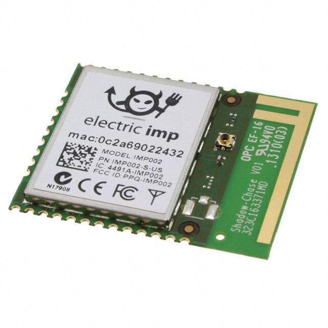
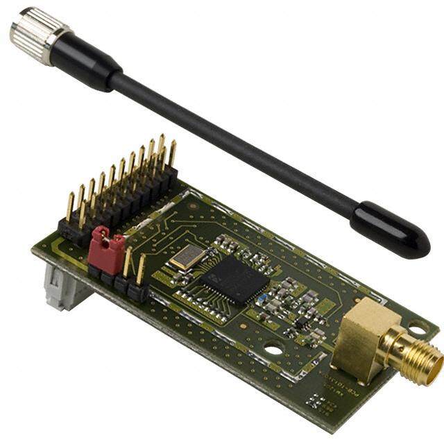
ICGOO电子元器件商城为您提供IMP002-S-US-TR由Electric Imp Inc设计生产,在icgoo商城现货销售,并且可以通过原厂、代理商等渠道进行代购。 IMP002-S-US-TR价格参考。Electric Imp IncIMP002-S-US-TR封装/规格:RF 收发器模块, WiFi 802.11b/g/n Transceiver Module 2.4GHz 集成式,跟踪 表面贴装。您可以下载IMP002-S-US-TR参考资料、Datasheet数据手册功能说明书,资料中有IMP002-S-US-TR 详细功能的应用电路图电压和使用方法及教程。
Electric Imp Inc. 的 IMP002-S-US-TR 是一款集成了Wi-Fi功能的无线通信模块,属于RF收发器模块的一种。该模块主要用于物联网(IoT)设备中,实现设备与互联网之间的无线数据传输。

其典型应用场景包括:

1. 智能家居设备:如智能照明、温控器、安防系统等,IMP002可通过Wi-Fi连接家庭网络,实现远程控制与数据上传。
2. 工业监测与控制系统:用于远程监测温度、湿度、压力等参数,并通过云端实现设备状态监控与管理。
3. 农业物联网:如土壤湿度监测、环境数据采集等,支持远程农业管理。
4. 医疗健康设备:如远程健康监测设备,将患者数据实时上传至云端供医生分析。
5. 零售与物流管理:用于智能货架、资产追踪、库存管理系统中,提升运营效率。

IMP002-S-US-TR模块内置处理器和Wi-Fi功能,支持TLS加密通信,具备较高的安全性和易集成性,适合需要稳定、安全无线连接的中小型物联网项目。
| 参数 | 数值 |
| 产品目录 | |
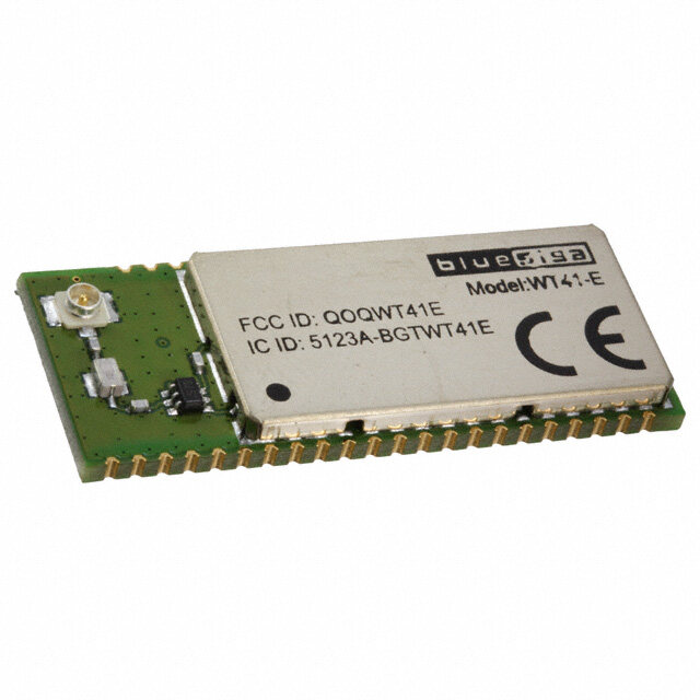
| 描述 | IMP 802.11B/G/N NODE MODULE |
| 产品分类 | RF 接收器、发射器及收发器的成品装置 |
| 品牌 | Electric Imp Inc |
| 数据手册 | |
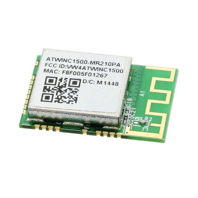
| 产品图片 |
|
| 产品型号 | IMP002-S-US-TR |
| rohs | 无铅 / 符合限制有害物质指令(RoHS)规范要求 |
| 产品系列 | - |
| 其它名称 | 1413-1001-2 |
| 功率-输出 | 16.75dBm |
| 功能 | 收发器, 802.11 b/g/n, WLAN |
| 应用 | 无线 LAN |
| 接口 | I²C, SPI, UART |
| 数据速率(最大值) | 1Mbps |
| 标准包装 | 500 |
| 灵敏度 | -97dBm |
| 特性 | - |
| 电压-电源 | 1.8 V ~ 3.6 V |
| 调制或协议 | 802.11 b/g/n |
| 频率 | 2.4GHz |


PDF Datasheet 数据手册内容提取
specification: imp002 version 20150716 http://www.electricimp.com
Electric Imp, inc. 1. Product description 1.1 General description The imp is a complete wireless network node in a module. It is available both in a memory card form-factor (imp001) and in a solder-down module form-factor (imp002). It works in conjunction with the imp service to allow easy connection of any device to the internet. There are two versions of imp002; the imp002-s uses the built-in antenna and the imp002-c uses an external antenna. This document covers specifications for both versions of the imp002. 1.2 Features • 802.11 b/g/n WiFi • 20MHz 11n channels, 1 x 1 • -97dBm typical sensitivity (1Mbps) • Integrated antenna with 2.5dBi max gain • TX power • 802.11b 16.5dBm +/-1.5dBm • 802.11g 14.0dBm +/-1.5dBm • 802.11n 12.75dBm +/-1.5dBm • 32-bit Cortex M3 processor • Robust embedded operating system with fail-safe firmware updates • Virtual machine for vendor firmware • LED drive for red/green status LEDs • Phototransistor input for our patent-pending BlinkUp technology to provide optical configuration • 12 user selectable I/Os • GPIO, PWM, Analog input & output • SPI (2 channels), UART (4.5 channels), I2C (2 channels) • Low power 6uA sleep mode • FCC, CE, IC C-Tick modular certification Ordering information Part number Description imp002-s-us-tr imp module with built-in antenna, US/CAN version, tape & reel imp002-s-eu-tr imp module with built-in antenna, EU/AUS/NZ version, tape & reel imp002-c-us-tr imp module which uses external antenna, US/CAN version, tape & reel imp002-c-eu-tr imp module which uses external antenna, EU/AUS/NZ version, tape & reel imp002 is rated at MSL 3 Electric Imp imp002 specification 2
Electric Imp, inc. 2. Imp terminology Term Description Electric Imp http://electricimp.com/aboutus/ The Application Programming Interface through which imp scripts may access hardware and API cloud functions Our patent-pending optical programming process for commissioning an imp using a smart BlinkUp device (phone or tablet) Initializing an imp by associating it with a user account and WiFi credentials, usually via Commissioning BlinkUp Blessing The process by which an imp card or module becomes associated with host hardware Server The electric imp cloud service with which imps communicate User-defined code that runs within a virtual machine. Device Firmware runs on the Electric Firmware Imp Hardware. Agent Firmware runs in the Electric Imp Cloud. A virtual machine within the Electric Imp Cloud. Each Electric Imp device is paired with exactly Agent one Agent. Integrated Development Environment. Used to develop and maintain your Electric Imp IDE Firmware. Push new code to devices from any place at any time. Ops Console Gain more insight into your factory production lines and scale to millions of devices Electric Imp imp002 specification 3
Electric Imp, inc. 3. Pin assignments 4. Pin description Pin Pin Name Description number 1, 7, 13, 17, 23– GND1 to 15 Ground 32, 35 18, 33 V Power Input DD 2 OPTO_BIAS Phototransistor power; connects to collector of phototransistor OPTO_IN Phototransistor signal; connects to emitter of phototransistor, which is connected to 6 ground with a bias resistor 3 LED_GREEN Green LED Output 4 LED_RED Red LED Output Active-high output for boost DC/DC enable. POWER_EN is driven high when the module requires a 2.5-3.3V power supply, which is typically when WiFi is active. This 5 POWER_EN pin has an internal pulldown while the imp is awake, which is disabled when the imp enters deep sleep. If this pin will be used while the imp is in deep sleep, an external pull-down is required. 34 V ADC reference voltage input. If unused, connect to V DDA DD Electric Imp imp002 specification 4
Electric Imp, inc. 8-12, 14- Pin1, Pin2, Pin5- I/O, please refer to Pin mux table 16, 19-22 PinE 4. LED drive The indicator LED should be bicolor, because red, green and amber (red+green) are used to indicate status. The LED drive pins will auto-detect common anode or common cathode parts. The detection is done by looking to see which way up the LED_RED pin is idling at boot; to ensure this works correctly, please place a 10kΩ resistor in parallel with the red LED. The current drive on these pins is 20mA maximum. Please refer to paragraph 12 for the recommended LEDs. Common anode diagram Common cathode diagram 5. Phototransistor The phototransistor is used to receive BlinkUp configuration data. The bias resistor connected between OPTO_IN and GND may need to be adjusted to ensure adequate sensitivity and response time - in general you need at least 500mV swing on the OPTO_IN pin between black and white states, with the worst (dimmest) BlinkUp sender you can find. End-user BlinkUp send data at between 30 and 60 bits per second, depending on the user’s device. For factory configuration, data is typically sent at 120 bits per second using red LED(s) in a test fixture. If your application does not require optical configuration, config can be sent electrically at 120 bits per second from another micro using the OPTO_IN pin. Please contact us for more details. Please refer to paragraph 12 for the recommended phototransistors. Electric Imp imp002 specification 5
Electric Imp, inc. Electric Imp imp002 specification 6
Electric Imp, inc. 6. External antenna The imp002-c is the version of imp002 that uses an external antenna. Please refer to paragraph 12 for the recommended antenna, which is used in our FCC approval. 7. Pin mux In addition to acting as a GPIO, each pin on the imp002 can be configured to one of several specialized functions. While pins may only have one function at a time, they may be reconfigured during run-time to change function as needed. For example, a pin may first be configured as a DAC and then reconfigured as an ADC. Additionally, not all the pins in a hardware function need to be assigned to that function. For example, pins 8 and 9 could be used as UART and pins 1 and 2 could be used as I2C. All I/O pins are initially tri-stated. The imp002 can be woken from low power sleep mode with a rising edge on PIN1. If this signal is pulsed, the minimum pulse width is 20ms. Pin GPIO UART I2C SPI DAC ADC PWM Pulse Count Wake PIN 1 Yes U1-CTS, U3-TX I1-SCL SPI1-SCLK Yes Yes Yes Yes Yes PIN 2 Yes U1-RTS, U3-RX I1-SDA SPI2-MISO Yes Yes PIN 5 Yes U2-TX SPI2-SCLK Yes Yes Yes PIN 6 Yes U6-TX PIN 7 Yes U2-RX SPI2-MOSI Yes Yes PIN 8 Yes U1-TX I2-SCL SPI1-MOSI Yes Yes PIN 9 Yes U1-RX I2-SDA SPI1-MISO Yes Yes PIN A Yes Yes PIN B Yes U4-RX Yes PIN C Yes Yes PIN D Yes PIN E Yes U6-RX Electric Imp imp002 specification 7
Electric Imp, inc. 8. Electrical characteristics Parameter Description Min Typ Max Unit. Operating temperature -20 55 ℃ VDD Operating voltage 1.8[1] 3.3 3.6 V VDDA Analog power input 1.8 VDD VDD V Normal operation, WiFi on 80 250[2] mA Normal operation, WiFi power-save 5 250[2] mA IDD mode enabled WiFi is off, processor sleep, RTC on, 6 µA nvram preserved IDDA Current input on VDDA 70 500 µA VIH I/O input high level voltage 0.7VDD 3.6 V VIL I/O input low level voltage VSS-0.3 0.3VDD V Output current on any single I/O pin -8 8 mA Output current on LED_RED pin -20 20 mA IOUT Output current on LED_GREEN pin -20 20 mA Total output current on all I/O pins -80 80 mA including LED_RED & LED_GREEN I/O input leakage current VSS ≦ VIN ≦ VDD 4 µA Pins 1 to 9 20 pF Load capacitance Pins A to E 5 pF [1] WiFi requires 2.5v minimum for operation, but user code can run at 1.8v. The POWER_EN pin is driven to enable an external boost converter that will provide 2.5v+ during WiFi usage. [2] 250mA current is during worst-case TX events. These are a maximum of ~4.8ms long (802.11b 1Mbps) Electric Imp imp002 specification 8
Electric Imp, inc. 9. Typical Application Circuit Electric Imp imp002 specification 9
Electric Imp, inc. 10. Package outline PCB dimensions (all dimensions are in mm unless otherwise specified) Electric Imp imp002 specification 10
Electric Imp, inc. Overall module dimensions (all dimensions are in mm unless otherwise specified) Electric Imp imp002 specification 11
Electric Imp, inc. Tape & reel dimensions Electric Imp imp002 specification 12
Electric Imp, inc. Reel disk dimensions Electric Imp imp002 specification 13
Electric Imp, inc. 11. Recommended Footprint (all dimensions are in mm unless otherwise specified) Notes: 1. Copper under solder mask is allowed in the “No Exposed Copper” region. Vias, even with full tenting, should not be placed in this region. 2. The “Copper and FR4 Keepout” guideline only applies to imp002-s which uses the built-in antenna. Electric Imp imp002 specification 14
Electric Imp, inc. 12. Recommended Layout 1: imp002 recommended layout with ground pours hidden 2: imp002 recommended layout with ground pours shown Electric Imp imp002 specification 15
Electric Imp, inc. 3: imp002 recommended layout shown in 3D 4: imp002 recommended layout shown in 3D, bottom of board Electric Imp imp002 specification 16
Electric Imp, inc. Notes: 1. Do not place copper or board material in the antenna keepout area. 2. Ground planes must be poured on the top and bottom layer across the imp footprint, and stitched together with a row of vias between pin 1 and pin 35 on the imp002. 3. Bypass and filter capacitors should be placed as close as possible to the V and V pins. DD DDA Electric Imp imp002 specification 17
Electric Imp, inc. 13. Recommended components Bi-color LED Manufacturer Manufacturer’s part number Surface mount SunLED XZMDKVG59W-1 top-view Liteon LTST-C195KGJRKT SunLED XZMDKVG88W side-view Bivar SM1204BC Through-hole SunLED XLMDKVG34M 3mm Liteon LTL1BEKVJNN Phototransistor Manufacturer Manufacturer’s part number Surface mount Everlight PT17-21C/L41/TR8 top-view Fairchild KDT00030TR SunLED XZRNI56W-1 side-view Everlight PT12-21C/TR8 Through-hole SunLED XRNI30W-1 3mm Honeywell SDP8405-003 Antenna Manufacturer Manufacturer’s part number for imp002-c-xx Mag Layers EDA-8709-2G4R2-A37 FCC Caution: To assure continued compliance, (example - use only shielded interface cables when connecting to computer or peripheral devices). Any changes or modifications not expressly approved by the party responsible for compliance could void the user’s authority to operate this equipment. This device complies with Part 15 of the FCC Rules. Operation is subject to the following two conditions: (1) This device may not cause harmful interference, and (2) this device must accept any interference received, including interference that may cause undesired operation. Electric Imp imp002 specification 18
Electric Imp, inc. 14. Reflow Solder Profile 240° to 250° 3s Max 220° 180° (Max) C 150° (Min) s e e r g e D Pre-heating Reflow 120s Max 60s Max Electric Imp imp002 specification 19
Electric Imp, inc. Version Change description 20121217 updated mechanical drawings to reflect the smaller coax connector 20130103 updated recommended footprint to have a cleaner look 20130122 changed PIN 10 to 14 to PIN A to E 20130218 added FCC caution statement 20130219 added TX power in paragraph 1.2 20130221 updated TX power values 20130312 PWM was incorrectly listed as a pinmux option for PINA/PINB 20130313 Removed bogus U1-RX from PIND. added suggested opto components in paragraph 10 20130321 added application diagrams & t&r info 20130429 added MSL info & change VREF to VDDA 20130605 added common cathode diagram, updated overall module tolerances 20130611 updated electrical characteristics table 20130710 added IDDA typ value and reel disk drawing 20130819 added ordering information table, added paragraph 7 and amended paragraph 12 20140224 updated tape & reel info due to new packaging 20140225 Changed source format, updated branding. 20140226 Added application circuit and recommended layout 20140616 Fixed error in BlinkUp section: please use 10kΩ resistor across LED_RED. 20140722 Added Solder Profile 20141012 Removed Kingbright APT2012P3BT phototransistor rec, added Fairchild KDT00030TR 20150716 Clarified internal pulldown behavior on POWER_EN pin Electric Imp imp002 specification 20