ICGOO在线商城 > IFX27001TFV
 Datasheet下载
- 型号: IFX27001TFV
- 制造商: Infineon
- 库位|库存: xxxx|xxxx
- 要求:
| 数量阶梯 | 香港交货 | 国内含税 |
| +xxxx | $xxxx | ¥xxxx |
查看当月历史价格
查看今年历史价格
IFX27001TFV产品简介:
ICGOO电子元器件商城为您提供IFX27001TFV由Infineon设计生产,在icgoo商城现货销售,并且可以通过原厂、代理商等渠道进行代购。 提供IFX27001TFV价格参考以及InfineonIFX27001TFV封装/规格参数等产品信息。 你可以下载IFX27001TFV参考资料、Datasheet数据手册功能说明书, 资料中有IFX27001TFV详细功能的应用电路图电压和使用方法及教程。
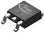
IFX27001TFV 是英飞凌(Infineon Technologies)推出的高性能线性稳压器(LDO),采用PG-TO263-7(即TO-263-7)封装,具有高精度、低噪声、高PSRR(电源抑制比)和优异的瞬态响应特性。其典型输入电压范围为2.95 V 至 40 V,输出电压可调(通过外部电阻分压器设定),最大输出电流达1.5 A,静态电流仅约35 µA(关断模式下低至1 µA),支持使能(EN)控制与电源良好(PG)信号输出。

该器件主要面向对供电质量要求严苛的汽车电子与工业应用:
✅ 车载信息娱乐系统(IVI):为DSP、音频ADC/DAC、触摸控制器等敏感模拟/混合信号电路提供低噪声、高稳定性的后级稳压电源;
✅ 高级驾驶辅助系统(ADAS):如摄像头模组、雷达传感器中的图像信号处理器(ISP)、MCU核心电源,需低纹波与强抗扰能力;
✅ 车身电子模块:如网关ECU、座椅/灯光控制单元中,为CAN/LIN收发器、EEPROM或精密传感器供电;
✅ 工业控制与医疗设备:适用于PLC I/O模块、便携式诊断设备等需宽输入电压、高可靠性及AEC-Q100 Grade 1(−40°C 至 +125°C)认证的场景。

其集成过流、过热与反向电流保护,并通过汽车级认证(AEC-Q100),确保在严苛温变、振动及电气干扰环境下长期稳定运行。
| 参数 | 数值 |
| 产品目录 | 集成电路 (IC)半导体 |
| 描述 | IC REG LDO ADJ 1A TO252-3低压差稳压器 Linear Voltage Regulator |
| 产品分类 | |
| 品牌 | Infineon Technologies |
| 产品手册 | |
| 产品图片 |
|
| rohs | 符合RoHS无铅 / 符合限制有害物质指令(RoHS)规范要求 |
| 产品系列 | 电源管理 IC,低压差稳压器,Infineon Technologies IFX27001TFV- |
| 数据手册 | http://www.infineon.com/dgdl/Infineon-IFX27001-DS-v01_01-en.pdf?folderId=db3a30431ff988150120802bce1d257a&fileId=db3a304320d39d590120f62f022a6a03&ack=t |
| 产品型号 | IFX27001TFV |
| 产品种类 | 低压差稳压器 |
| 供应商器件封装 | PG-TO252-3 |
| 其它名称 | IFX27001TFVINDKR |
| 包装 | Digi-Reel® |
| 商标 | Infineon Technologies |
| 回动电压—最大值 | 1 V |
| 安装类型 | 表面贴装 |
| 安装风格 | SMD/SMT |
| 封装 | Reel |
| 封装/外壳 | TO-252-3,DPak(2 引线+接片),SC-63 |
| 封装/箱体 | PG-TO-252-3 |
| 工作温度 | -40°C ~ 125°C |
| 工厂包装数量 | 2500 |
| 最大工作温度 | + 125 C |
| 最大输入电压 | 40 V |
| 标准包装 | 1 |
| 电压-跌落(典型值) | 1.3V @ 1A |
| 电压-输入 | 最高 40 V |
| 电压-输出 | 可调 |
| 电流-输出 | 1A |
| 电流-限制(最小值) | 1A |
| 稳压器拓扑 | 正,可调式 |
| 稳压器数 | 1 |
| 系列 | IFX27001 |
| 负载调节 | 0.5 mV |
| 输出电压 | Adj |
| 输出电流 | 1 A |
| 输出端数量 | 1 Output |
| 输出类型 | Adjustable |
| 零件号别名 | IFX27001TFVATMA1 SP000624090 |


- 商务部:美国ITC正式对集成电路等产品启动337调查
- 曝三星4nm工艺存在良率问题 高通将骁龙8 Gen1或转产台积电
- 太阳诱电将投资9.5亿元在常州建新厂生产MLCC 预计2023年完工
- 英特尔发布欧洲新工厂建设计划 深化IDM 2.0 战略
- 台积电先进制程称霸业界 有大客户加持明年业绩稳了
- 达到5530亿美元!SIA预计今年全球半导体销售额将创下新高
- 英特尔拟将自动驾驶子公司Mobileye上市 估值或超500亿美元
- 三星加码芯片和SET,合并消费电子和移动部门,撤换高东真等 CEO
- 三星电子宣布重大人事变动 还合并消费电子和移动部门
- 海关总署:前11个月进口集成电路产品价值2.52万亿元 增长14.8%


PDF Datasheet 数据手册内容提取
IFX27001 Linear Voltage Regulator IFX27001TFV15 IFX27001TFV18 IFX27001TFV26 IFX27001TFV33 Data Sheet Rev. 1.01, 2009-10-19 Standard Power
Linear Voltage Regulator IFX27001 1 Overview Features • 1.5V, 1.8V, 2.6V, 3.3 V, 5.0V or Adj. output voltage • 1.0 A output current • Low dropout voltage, 1V (typ.) • Short circuit protection • Overtemperature protection • Input Votlage up to 40 V • Wide temperature range of T = -40 to 125 °C j • Green Product (RoHS compliant) PG-TO252-3 Applications • Manufacturing Automation • Appliances • HDTV Televisions • Game Consoles • Network Routers For automotive and transportation applications, please refer to the Infineon TLE and TLF voltage regulator series Description The IFX27001 is a monolithic integrated NPN type voltage regulator that can supply loads up to 1.0 A. The chip is housed in a surface mount PG-TO252-3 package (DPAK). It is designed to supply microprocessor systems or other loads under the severe conditions and therefore it is equipped with additional protection against overload, short circuit and overtemperature. An large input voltage V in the range of (V + V ) < V < 40 V is regulated to V . The dropout voltage V ranges I Q DR I Q DR from 1.1 V to 1.4 V depending on the load current level. The device operates in the temperature range of T = -40 to 125 °C.. j Type Package Marking IFX27001TFV15 PG-TO252-3 2700115 IFX27001TFV18 PG-TO252-3 2700118 IFX27001TFV26 PG-TO252-3 2700126 IFX27001TFV33 PG-TO252-3 2700133 IFX27001TFV50 PG-TO252-3 2700150 IFX27001TFV PG-TO252-3 27001V Data Sheet 2 Rev. 1.01, 2009-10-19
IFX27001 Block Diagram 2 Block Diagram I Q Control with Overtemperature Protection; Internal Overcurrent Reference Protection GND AES02840 Figure1 Block Diagram for Fixed Output Voltage (1.5V, 1.8V, 2.6V, 3.3V, 5.0V) I Q Control with Overtemperature Adjust Protection; Internal Overcurrent Reference Protection AES02839 Figure2 Block Diagram for Adjustable Output Voltage Data Sheet 3 Rev. 1.01, 2009-10-19
IFX27001 Pin Configuration 3 Pin Configuration 3.1 Pin Assignment Fixed Output Adjustable Output Voltage Version Voltage Version Q Q 1 1 Q Q GND I ADJ I AEP02817 AEP02821 Figure3 Pin Configuration (top view) 3.2 Pin Definitions and Functions Table1 Pin Definitions and Functions Fixed Output Voltage Versions Pin No. Symbol Function 1 GND Ground 2, Tab Q Output; Connect a capacitor C ≥10 µF with ESR ≤ 10Ω between pin Q and GND Q Connect to heatsink area. 3 I Input Table2 Pin Definitions and Functions Adjustable Output Version Pin No. Symbol Function 1 ADJ Adjust; defines output voltage by external voltage divider between Q, ADJ and GND. 2, Tab Q Output; the output voltage is defined by the external voltage divider between Q, Adjust and Ground. Connect a capacitor C ≥10 µF with ESR ≤ 10Ω between pin Q and GND Q Connect to heatsink area. 3 I Input Data Sheet 4 Rev. 1.01, 2009-10-19
IFX27001 General Product Characteristics 4 General Product Characteristics 4.1 Absolute Maximum Ratings Absolute Maximum Ratings1) T =-40°C to 150 °C; all voltages with respect to ground, (unless otherwise specified) j Pos. Parameter Symbol Limit Values Unit Test Condition Min. Max. Input I 4.1.1 Voltage V -0.3 40 V – I Input - Output Voltage Differential (Applies to Adjustable Output Version Only)I 4.1.2 Voltage V - V -0.3 40 V – I Q Output Q 4.1.3 Voltage V -0.3 40 V – Q Temperature 4.1.4 Junction temperature T -40 150 °C – j 4.1.5 Storage temperature T -50 150 °C – stg ESD Susceptibility 4.1.6 ESD Absorption V -2 2 kV Human Body Model ESD,HBM (HBM)2) 4.1.7 V -500 500 V Charge Device ESD,CDM Model (CDM)3) 4.1.8 -750 750 V Charge Device Model (CDM)3) at corner pins 1) not subject to production test, specified by design 2) ESD susceptibility Human Body Model “HBM” according to AEC-Q100-002 - JESD22-A114 3) ESD susceptibility Charged Device Model “CDM” according to ESDA STM5.3.1 Note:Stresses above the ones listed here may cause permanent damage to the device. Exposure to absolute maximum rating conditions for extended periods may affect device reliability. Note:Integrated protection functions are designed to prevent IC destruction under fault conditions described in the data sheet. Fault conditions are considered as “outside” normal operating range. Protection functions are not designed for continuous repetitive operation. Data Sheet 5 Rev. 1.01, 2009-10-19
IFX27001 General Product Characteristics 4.2 Functional Range Pos. Parameter Symbol Limit Values Unit Remarks Min. Max. 4.2.1 Input voltage V V + V 40 V I I DR 4.2.2 Junction temperature T -40 125 °C – j Note:Within the functional or operating range, the IC operates as described in the circuit description. The electrical characteristics are specified within the conditions given in the Electrical Characteristics table. 4.3 Thermal Resistance Note:This thermal data was generated in accordance with JEDEC JESD51 standards. For more information, go to www.jedec.org. Pos. Parameter Symbol Limit Values Unit Conditions Min. Typ. Max. PG-TO252-3 4.3.1 Junction to Case1) R – 4 – K/W measured to heat thJC slug 4.3.2 Junction to Ambient1) R – 27 – K/W 2) thJA 4.3.3 R – 57 – K/W 300mm² heatsink thJA area3) 4.3.4 R – 42 – K/W 600mm² heatsink thJA area3) 1) Not subject to production test, specified by design. 2) Specified R value is according to Jedec JESD51-2,-5,-7 at natural convection on FR4 2s2p board; The Product thJA (Chip+Package) was simulated on a 76.2 x 114.3 x 1.5 mm³ board with 2 inner copper layers (2 x 70µm Cu, 2 x 35µm Cu). Where applicable a thermal via array under the exposed pad contacted the first inner copper layer. 3) Specified R value is according to Jedec JESD 51-3 at natural convection on FR4 1s0p board; The Product thJA (Chip+Package) was simulated on a 76.2 × 114.3 × 1.5 mm3 board with 1 copper layer (1 x 70µm Cu). Data Sheet 6 Rev. 1.01, 2009-10-19
IFX27001 Electrical Characteristics 5 Electrical Characteristics 5.1 Electrical Characteristics Voltage Regulator Table3 Electrical Characteristics IFX27001TFV DV (adjustable output voltage) -40°C<T <125°C; V - V = 13.5V, I = 10mA; unless otherwise specified j I Q Q Parameter Symbol Limit Values Unit Measuring Conditions min. typ. max. Reference voltage V 1) 1.20 1.25 1.30 V – REF Line regulation ΔV – 0.5 1.50 % 2) 3 V ≤ (V – V ) ≤ 40 V Q I Q Load regulation ΔV – 0.2 0.4 % 2) 10 mA ≤ I ≤ 800mA; 4) Q Q V = 3.0V; V = V I Q REF – 0.25 0.5 % 2) 10 mA ≤ I ≤ 1.0A; 4) Q V = 3.0V; V = V I Q REF Dropout voltage V – 1.00 1.20 V I =100 mA 3) DR Q – 1.05 1.30 V I =500 mA 3) Q – 1.10 1.35 V I =800 mA 3) Q – 1.30 1.40 V I =1.0A 3) Q Current consumption I – 100 120 μA I =10mA; q Q I =I –I q I Q Adjust current I – 75 120 μA I =10mA ADJ Q Adjust current change ΔI – 2 5 μA I =10mA ADJ Q 3 V ≤ (V – V ) ≤ 40 V 4) I Q – 2 5 μA 10 mA ≤ I ≤ 200 mA; Q V - V = 3 V 4) I Q Temperature stability – – 0.6 – % 5) Minimum load current 6) I – 1 5 mA V < 40 V; Q I V = V Q REF Current limit I 1000 – 2200 mA 1.4V < V - V < 18V; Qmax I Q V = V -100 mV Q nom 50 200 – mA V = 40 V; I V = V -100 mV Q nom T = 25 °C j RMS Output Noise – – 30 – ppm ppm of V ; T = 25 °C; Q j 10 Hz ≤ f ≤ 10kHz 5) Power Supply Ripple Rejection PSRR – 65 – dB V = 10 V, f = 120 Hz, Q r V =0.5V , C = 0 μF 5) r PP ADJ – 65 – dB V = 10 V, f = 120 Hz, Q r V =0.5V , C = 10 μF r PP ADJ 5) 1) V = V –V REF Q ADJ 2) Related to V measured at constant junction Temperature Q, 3) Dropout voltage measured when the output voltage has dropped 100mV from the nominal value obtained at V =V . Q REF 4) Constant Junction Temperature 5) Not subject to production test - specified by design. 6) Minimum Output Current to maintain regulation Data Sheet 7 Rev. 1.01, 2009-10-19
IFX27001 Electrical Characteristics Table4 Electrical Characteristics IFX27001TFV15DV15 (1.5V fixed output voltage) -40°C<T <125°C; V =13.5V, I = 10mA; unless otherwise specified j I Q Parameter Symbol Limit Values Unit Measuring Conditions min. typ. max. Output voltage V 1.45 1.5 1.55 V 10 mA ≤ I ≤ 1000 mA; Q Q 2.9V ≤ V ≤ 16 V I – 1.5 – V 10 mA ≤ I ≤ 1000 mA; Q 16 V ≤ V ≤ 40 V 1) I Line regulation ΔV – 4.8 22.5 mV 2.9 V ≤ V ≤ 40 V Q I Load regulation ΔV – 2.6 5.2 mV 10 mA ≤ I ≤ 800mA; 2) Q Q V = V + V I Qnom DR – 3.1 6.25 mV 10 mA ≤ I ≤ 1.0A 2) Q V = V + V I Qnom DR Dropout voltage V – 1.00 1.20 V I =100 mA 3) DR Q – 1.05 1.30 V I =500 mA 3) Q – 1.10 1.35 V I =800 mA 3) Q – 1.30 1.40 V I =1.0A 3) Q Current consumption I – 0.8 1.6 mA I =10mA q Q I =I –I q I Q Temperature stability – – 8.8 – mV 4) Current limit I 100 0 – 2200 mA V – V <18V; Qmax I Q V = V - 100 mV Q nom 50 200 – mA V = 40 V; I V = V - 100 mV Q nom T = 25 °C j RMS Output Noise – – 30 – ppm ppm of V , T = 25 °C Q j 10 Hz ≤ f ≤ 10 kHz 4) Power Supply Ripple Rejection PSRR – 65 – dB f =120Hz, V=0.5V , r r PP C = 0 μF 4) ADJ – 65 – dB f = 120 Hz, V =0.5V , r r PP C = 10 μF 4) ADJ 1) Device is usable within given range without destruction, but the accuracy of the output voltage can only be guarantied in the range specified in the line above. 2) Measured at constant junction temperature 3) Dropout voltage measured when the output voltage has dropped 100mV from the nominal value. 4) Not subject to production test - specified by design. Data Sheet 8 Rev. 1.01, 2009-10-19
IFX27001 Electrical Characteristics Table5 Electrical Characteristics IFX27001TFV18DV18 (1.8V fixed output voltage) -40°C<T <125°C; V =13.5V, I = 10mA; unless otherwise specified j I Q Parameter Symbol Limit Values Unit Measuring Conditions min. typ. max. Output voltage V 1.75 1.8 1.85 V 10 mA ≤ I ≤ 1000 mA; Q Q 3.2V ≤ V ≤ 16 V I – 1.8 – V 10 mA ≤ I ≤ 1000 mA; Q 16 V ≤ V ≤ 40 V 1) I Line regulation ΔV – 7.2 27 mV 3.2 V ≤ V ≤ 40V Q I Load regulation ΔV – 3.4 7.6 mV 10 mA ≤ I ≤ 800mA 2) Q Q V=V + V I Qnom DR – 4.8 9 mV 10 mA ≤ I ≤ 1.0A 2) Q V=V + V I Qnom DR Dropout voltage V – 1.00 1.20 V I =100 mA 3) DR Q – 1.05 1.30 V I =500 mA 3) Q – 1.10 1.35 V I =800 mA 3) Q – 1.30 1.40 V I =1.0A 3) Q Current consumption I – 0.8 1.6 mA I =10mA q Q I =I –I q I Q Temperature stability – – 11 – mV 4) Current limit I 100 0 – 2200 mA V – V < 18V; Qmax I Q V = V - 100 mV Q nom 50 200 – mA V = 40 V; I V = V - 100 mV Q nom T = 25 °C j RMS Output Noise – – 30 – ppm ppm of V , T = 25 °C Q j 10 Hz ≤ f ≤ 10 kHz 4) Power Supply Ripple Rejection PSRR – 65 – dB f =120Hz; V = 0.5 V r r PP C = 0 μF 4) ADJ – 65 – dB f = 120 Hz; V =0.5 V , r r PP C = 10 μF 4) ADJ 1) Device is usable within given range without destruction, but the accuracy of the output voltage can only be guarantied in the range specified in the line above. 2) Measured at constant junction temperature 3) Dropout voltage measured when the output voltage has dropped 100mV from the nominal value. 4)Not subject to production test - specified by design. Data Sheet 9 Rev. 1.01, 2009-10-19
IFX27001 Electrical Characteristics Table6 Electrical Characteristics IFX27001TFV26DV26 (2.6V fixed output voltage) -40°C<T <125°C; V =13.5V, I = 10mA; unless otherwise specified j I Q Parameter Symbol Limit Values Unit Measuring Conditions min. typ. max. Output voltage V 2.52 2.60 2.68 V 10 mA ≤ I ≤ 1000 mA; Q Q 4.0V ≤ V ≤ 16 V I – 2.60 – V 10 mA ≤ I ≤ 1000 mA; Q 16 V ≤ V ≤ 40 V 1) I Line regulation ΔV – 11 40 mV 4.0 V ≤ V ≤ 40 V Q I Load regulation ΔV – 5 11 mV 10 mA ≤ I ≤ 800mA; 2) Q Q V = V + V I Qnom DR – 7 13 mV 10 mA ≤ I ≤ 1.0A 2) Q V =V + V I Qnom DR Dropout voltage V – 1.00 1.20 V I =100 mA 3) DR Q – 1.05 1.30 V I =500 mA 3) Q – 1.10 1.35 V I =800 mA 3) Q – 1.30 1.40 V I =1.0A 3) Q Current consumption; I – 0.8 1.6 mA I =10mA q Q I =I –I q I Q Temperature stability – – 16 – mV 4) Current limit I 100 0 – 2200 mA V – V <18V; Qmax I Q V = V - 100 mV Q nom 50 200 – mA V = 40 V; I V = V - 100 mV Q nom T = 25 °C j RMS Output Noise – – 30 – ppm ppm of V , T = 25 °C Q j 10 Hz ≤ f ≤ 10 kHz 4) Power Supply Ripple Rejection PSRR – 65 – dB f =120Hz, V=0.5V , r r PP C = 0 μF 4) ADJ – 65 – dB f = 120 Hz, V =0.5V , r r PP C = 10 μF 4) ADJ 1) Device is usable within given range without destruction, but the accuracy of the output voltage can only be guarantied in the range specified in the line above. 2) Measured at constant junction temperature 3) Dropout voltage measured when the output voltage has dropped 100mV from the nominal value. 4) Not subject to production test - specified by design. Data Sheet 10 Rev. 1.01, 2009-10-19
IFX27001 Electrical Characteristics Table7 Electrical Characteristics IFX27001TFV33DV33 (3.3V fixed output voltage) -40°C<T <125°C; V =13.5V, I = 10mA; unless otherwise specified j I Q Parameter Symbol Limit Values Unit Measuring Conditions Min. Typ. Max. Output voltage V 3.20 3.3 3.40 V 10 mA ≤ I ≤ 1000 mA; 4.7 Q Q V ≤ V ≤ 16 V I – 3.3 – V 10 mA ≤ I ≤ 1000 mA ; 16 Q V ≤ V ≤ 40 V 1) I Line regulation ΔV – 15 50 mV 4.7 V ≤ V ≤ 40 V Q I Load regulation ΔV – 6 13 mV 10 mA ≤ I ≤ 800 mA 2) Q Q V = V + V I Qnom DR – 8 16 mV 10 mA ≤ I ≤ 1.0 A 2) Q V = V + V I Qnom DR Dropout voltage V – 1.00 1.20 V I = 100 mA 3) DR Q – 1.05 1.30 V I = 500 mA 3) Q – 1.10 1.35 V I = 800 mA 3) Q – 1.30 1.40 V I = 1.0 A 3) Q Current consumption I – 0.8 1.6 mA I = 10 mA q Q I = I - I q I Q Temperature stability – – 20 – mV 4) Current limit I 1000 – 2200 mA V – V < 18V; Qmax I Q V = V - 100 mV Q nom 50 200 – mA V = 40 V; I V = V - 100 mV Q nom T = 25 °C j RMS Output Noise – – 30 – ppm ppm of V ; T = 25 °C; Q j 10 Hz ≤ f ≤ 10 kHz 4) Power Supply Ripple Rejection PSRR – 65 – dB f = 120 Hz; V = 0.5 Vpp; r r C = 0 μF 4) ADJ – 65 – dB f = 120 Hz; V = 0.5 Vpp; r r C = 10 μF 4) ADJ 1) Device is usable within given range without destruction, but the accuracy of the output voltage can only be guarantied in the range specified in the line above. 2) Measured at constant junction temperature. 3) Dropout voltage measured when the output voltage has dropped 100mV from the nominal value. 4) Not subject to production test - specified by design. Data Sheet 11 Rev. 1.01, 2009-10-19
IFX27001 Electrical Characteristics Table8 Electrical Characteristics IFX27001TFV50DV50 (5.0V fixed output voltage) -40°C<T <125°C; V =13.5V, I = 10mA; unless otherwise specified j I Q Parameter Symbol Limit Values Unit Measuring Conditions min. typ. max. Output voltage V 4.85 5.00 5.15 V 10 mA ≤ I ≤ 1000mA; Q Q 6.4V ≤ V ≤ 16V I – 5.00 – V 10 mA ≤ I ≤ 1000mA; Q 16V ≤ V ≤ 40 V 1) I Line regulation ΔV – 20 75 mV 6.4V ≤ V ≤ 40V Q I Load regulation ΔV – 9 20 mV 10 mA ≤ I ≤ 800mA 2) Q Q V = V + V I Qnom DR – 12 24 mV 10 mA ≤ I ≤ 1.0A 2) Q V = V + V I Qnom DR Dropout voltage V – 1.00 1.20 V I =100 mA 3) DR Q – 1.05 1.30 V I =500 mA 3) Q – 1.10 1.35 V I =800 mA 3) Q – 1.30 1.40 V I =1.0A 3) Q Current consumption I – 0.8 1.6 mA I =10mA q Q I =I –I q I Q Temperature stability – – 30 – mV 4) Current limit I 100 0 – 2200 mA V – V <18V; Qmax I Q V = V - 100 mV Q nom 50 200 – mA V = 40 V; I V = V - 100 mV Q nom T = 25 °C j RMS Output Noise – – 30 – ppm ppm of V , T = 25 °C Q j 10 Hz ≤ f ≤ 10 kHz 4) Power Supply Ripple Rejection PSRR – 65 – dB f =120Hz, V=0.5V , r r PP C = 0 μF 4) ADJ – 65 – dB f =120Hz, V=0.5V , r r PP C = 10 μF 4) ADJ 1) Device is usable within given range without destruction, but the accuracy of the output voltage can only be guarantied in the range specified in the line above. 2) Measured at constant junction temperature 3) Dropout voltage measured when the output voltage has dropped 100mV from the nominal value. 4) Not subject to production test - specified by design. Data Sheet 12 Rev. 1.01, 2009-10-19
IFX27001 Electrical Characteristics IFX27001TFV I I I Q I Q V 3 2 I C I C 100 nF Q V Q 1 GND I GND IFX27001TFV I I I I Q Q V 3 2 I C I C 100 nF Q R 1 1 V Q ADJ I ADJ R 2 Figure4 Measuring Circuit of fixed output voltage versions and adjustable output voltage version Data Sheet 13 Rev. 1.01, 2009-10-19
IFX27001 Electrical Characteristics 5.2 Typical Performance Characteristics Voltage Regulator Current Consumption I versus Current Consumption I versus q q Junction Temperature T Input Voltage V J I 1_Iq-Tj.vsd 3_Iq-VI.vsd I [mA] I [mA] q q VI = 13.5V VI = 13.5V I = 10mA Q 10 10 IQ = 1mA I = 10mA Q I = 500mA Q I = 1000mA Q 1 1 5.0V-Version 3.3V-Version 2.6V-Version 0.1 0.1 1.8V-Version 1.5V-Version 0.01 0.01 -40 -20 0 20 40 60 80 100 120 140 0 10 20 30 40 T [°C] V [V] j I Current Consumption I versus Adjust Current I and Reference Voltage V q ADJ Ref Output Current I versus Junction Temperature T Q J 2_IQ-IQ.VSD 1.248 4_IADJ_TJ.VSD 76 I [mA] q VREF IQ=10mA IADJ [V] [µA] 10 IADJ T = 150°C j 1.244 74 T = 25°C j T = -40°C j 1 1.242 V 73 REF 1.24 72 0.1 1.238 71 1.236 70 0.01 -40 -20 0 20 40 60 80 100 120 140 0.0001 0.001 0.01 0.1 1 IQ [A] Tj[°C] Data Sheet 14 Rev. 1.01, 2009-10-19
IFX27001 Electrical Characteristics Output Voltage V versus Power Supply Ripple Rejection versus Q InputVoltage V Frequency I 6.00 11_VI-VQ.vsd 90 13_PSRR.VSD T = 25 °C V = 0.5 V V [V] a PSRR RIPPLE Q 5.0V-Version IQ = 100mA [dB] VIN = 13.5 V C = 10 µF Tantalum ADJ I = 10mA T = 25 °C Q a I = 10 mA 4.00 70 Q 3.3V-Version I = 125 mA Q 3.00 2.6V-Version 60 I = 250 mA Q I = 500 mA 2.00 1.8V-Version 50 Q I = 1000 mA Q 1.5V-Version 1.00 40 I = 500mA I = 1000mA Q Q 0 10 20 30 40 10 100 1k 10k 100k V [V] f [Hz] I Stability Region: Equivalent Serial Resistor ESR Power Supply Ripple Rejection versus versus Output Current I Frequency Q 12_ESR-IQ.VSD 13_PSRR.VSD 1000 90 ESRCQ CTjQ = = - 4100.µ..F150°C P[SdBR]R VVRIP P=L E1 3=. 50 .V5 V [Ω] V = 6...25V IN I CADJ = 10 µF Tantalum T = 25 °C a 100 I = 10 mA Q 70 C = 2.2µF Q T = -40...150°C j I = 125 mA V = 6...25V Q 10 I 60 I = 250 mA Q I = 500 mA Stable 50 Q I = 1000 mA Region Q 1 40 0.1 0.1 1 10 100 1000 10 100 1k 10k 100k I [mA] f [Hz] Q Data Sheet 15 Rev. 1.01, 2009-10-19
IFX27001 Application Information 6 Application Information Note:The following information is given as a hint for the implementation of the device only and shall not be regarded as a description or warranty of a certain functionality, condition or quality of the device. IFX27001TFV I Q V 3 2 V I Q C C C I1 I2 Q2 1 GND IFX27001TFV I Q V 3 2 V I Q C C C I1 I2 Q2 R 1 V - V = V 1 Q ADJ REF ADJ I ADJ R C 2 ADJ AES02815 Figure5 Application Diagram Application Hints Adjustable Version At the fixed voltage IFX27001 devices, the output voltage is divided internally and compared to an internal reference of 1.25V typical. The regulation loop controls the output voltage to achieve the output voltage of 5V, 3.3V, 2.6V, 1.8V or 1.5V. The variable version compares the voltage difference between the adjust pin ADJ and the output pin Q to the internal reference of typically 1.25V. The output voltage is adjusted by an external voltage divider between Q, ADJ and GND and calculates: R V = V ×⎛1+ ----2-⎞ +I ×R Q REF ⎝ R ⎠ ADJ 2 1 Data Sheet 16 Rev. 1.01, 2009-10-19
IFX27001 Application Information For the variable regulator IFX27001TFV, a minimum load current of 5mA is necessary in order to keep the output voltage regulated. If the application does not assure this minimum load requirement, the output voltage divider should be dimensioned sufficiently low-ohmic: R ≤240 Ω. 1 For the variable voltage type an additional decoupling a capacitor C at the adjust pin improves the ripple ADJ rejection ratios. Placing C requires an increased output capacitance of C ≥22 µF. ADJ Q Output The output current limitation is reduced as a function of the input voltage for high input voltages above 25V. The IFX27001 requires a 10µF output capacitor with 0.1Ω ≤ ESR ≤ 10Ω for the stability of the regulation loop. At the input of the regulator a capacitor is necessary for compensation of line influences. A series diode should be used to eliminate negative voltages from the input. As a minimum, a 100nF ceramic input capacitor should be used. If the regulator is used in an environment with long input lines, an input capacitance of 10µF is recommended. Data Sheet 17 Rev. 1.01, 2009-10-19
IFX27001 Package Outlines 7 Package Outlines +0.15 6.5 -0.05 A +0.05 2.3 5.4±0.1 -0.10 (5) B 0.5+0.08 -0.04 1 0. ± 1 +0.20 0.9 -0.01 9.98±0.5 6.22-0.2 (4.24) 0.8±0.15 0..N..0.15 MI 1 0.15 MAX. 3x 0.5 per side +0.08 0.75±0.1 0.5-0.04 2.28 0.1 B 4.57 0.25 M A B All metal surfaces tin plated, except area of cut. Figure6 PG-TO252-3 Green Product (RoHS compliant) To meet the world-wide customer requirements for environmentally friendly products and to be compliant with government regulations the device is available as a green product. Green products are RoHS-Compliant (i.e Pb-free finish on leads and suitable for Pb-free soldering according to IPC/JEDEC J-STD-020). For further information on packages, please visit our website: http://www.infineon.com/packages. Dimensions in mm Data Sheet 18 Rev. 1.01, 2009-10-19
IFX27001 Revision History 8 Revision History Revision Date Changes 1.01 2009-10-19 Coverpage changed Overview page: Inserted reference statement to TLE/TLF series. 1.0 2009-04-28 Initial Release Data Sheet 19 Rev. 1.01, 2009-10-19
Edition 2009-10-19 Published by Infineon Technologies AG 81726 Munich, Germany © 2009 Infineon Technologies AG All Rights Reserved. Legal Disclaimer The information given in this document shall in no event be regarded as a guarantee of conditions or characteristics. With respect to any examples or hints given herein, any typical values stated herein and/or any information regarding the application of the device, Infineon Technologies hereby disclaims any and all warranties and liabilities of any kind, including without limitation, warranties of non-infringement of intellectual property rights of any third party. Information For further information on technology, delivery terms and conditions and prices, please contact the nearest Infineon Technologies Office (www.infineon.com). Warnings Due to technical requirements, components may contain dangerous substances. For information on the types in question, please contact the nearest Infineon Technologies Office. Infineon Technologies components may be used in life-support devices or systems only with the express written approval of Infineon Technologies, if a failure of such components can reasonably be expected to cause the failure of that life-support device or system or to affect the safety or effectiveness of that device or system. Life support devices or systems are intended to be implanted in the human body or to support and/or maintain and sustain and/or protect human life. If they fail, it is reasonable to assume that the health of the user or other persons may be endangered.
Mouser Electronics Authorized Distributor Click to View Pricing, Inventory, Delivery & Lifecycle Information: I nfineon: IFX27001TF V15 IFX27001TF V33 IFX27001TFV