ICGOO在线商城 > Labels, Signs, Barriers, Identification > Accessories > HW-RIBBON14
 Datasheet下载
- 型号: HW-RIBBON14
- 制造商: Xilinx
- 库位|库存: xxxx|xxxx
- 要求:
| 数量阶梯 | 香港交货 | 国内含税 |
| +xxxx | $xxxx | ¥xxxx |
查看当月历史价格
查看今年历史价格
HW-RIBBON14产品简介:
ICGOO电子元器件商城为您提供HW-RIBBON14由Xilinx设计生产,在icgoo商城现货销售,并且可以通过原厂、代理商等渠道进行代购。 HW-RIBBON14价格参考。XilinxHW-RIBBON14封装/规格:Accessories, Parallel Cable IV and MultiPRO - Cable Assembly。您可以下载HW-RIBBON14参考资料、Datasheet数据手册功能说明书,资料中有HW-RIBBON14 详细功能的应用电路图电压和使用方法及教程。
Xilinx Inc. 的 HW-RIBBON14 是一款用于 FPGA 开发的配件(分类:Accessories),主要用于连接 FPGA 开发板与外部扩展模块或目标系统。该型号为 14 针带状电缆,常用于信号传输和调试接口,典型应用场景包括:

1. 开发板与子板连接:HW-RIBBON14 可将 Xilinx FPGA 开发板(如 Spartan 或 Artix 系列开发套件)与各类 I/O 扩展子板、传感器板或原型板相连,实现数据与控制信号的可靠传输。

2. 调试与编程接口:在系统调试过程中,该线缆可用于连接板载 JTAG 或其他调试接口,辅助进行 FPGA 配置、固件下载和硬件诊断。

3. 教学与实验平台:广泛应用于高校实验室和培训课程中,帮助学生理解 FPGA 外设连接与嵌入式系统设计。

4. 工业原型开发:在工业控制、通信设备等领域的原型设计中,用于快速搭建 FPGA 与外围电路的物理连接,缩短开发周期。

HW-RIBBON14 具有良好的电气性能和机械稳定性,适用于低速至中速数字信号传输,是 Xilinx 生态系统中常用的互连配件之一。
| 参数 | 数值 |
| 产品目录 | 编程器,开发系统 |
| 描述 | CABLE FOR CABLE IV OR MULTIPRO |
| 产品分类 | |
| 品牌 | Xilinx Inc |
| 数据手册 | |
| 产品图片 |
|
| 产品型号 | HW-RIBBON14 |
| rohs | 含铅 / 不符合限制有害物质指令(RoHS)规范要求 |
| 产品系列 | - |
| 产品目录页面 | |
| 其它名称 | 122-1476 |
| 标准包装 | 1 |
| 特色产品 | http://www.digikey.cn/product-highlights/cn/zh/analog-devices-solutions-for-xilinx-fpgas/3178 |
| 配件类型 | 缆线组件 |
| 配套使用产品/相关产品 | 并行线缆 IV 和 MultiPRO |


- 商务部:美国ITC正式对集成电路等产品启动337调查
- 曝三星4nm工艺存在良率问题 高通将骁龙8 Gen1或转产台积电
- 太阳诱电将投资9.5亿元在常州建新厂生产MLCC 预计2023年完工
- 英特尔发布欧洲新工厂建设计划 深化IDM 2.0 战略
- 台积电先进制程称霸业界 有大客户加持明年业绩稳了
- 达到5530亿美元!SIA预计今年全球半导体销售额将创下新高
- 英特尔拟将自动驾驶子公司Mobileye上市 估值或超500亿美元
- 三星加码芯片和SET,合并消费电子和移动部门,撤换高东真等 CEO
- 三星电子宣布重大人事变动 还合并消费电子和移动部门
- 海关总署:前11个月进口集成电路产品价值2.52万亿元 增长14.8%


PDF Datasheet 数据手册内容提取
36 Platform Cable USB II DS593 (v1.5.1) August 6, 2018 Features (cid:129) High-performance FPGA and PROM programming and (cid:129) Reliable configuration (cid:129) Backwards compatibility with Platform Cable USB, (cid:129) Includes innovative FPGA-based acceleration including Pb-Free (RoHS-compliant) firmware encapsulated in a small form factor pod (cid:129) USB Integrators Forum (USB-IF) certified attached to the cable (cid:129) CE and FCC compliant (cid:129) Leverages high-speed slave-serial mode (cid:129) Leverages industry standards, including JTAG programming interface boundary-scan IEEE 1149.1, SPI and USB 2.0 Note: Slave-serial mode is supported in Xilinx® (cid:129) Programs and configures all Xilinx devices iMPACT software v10.1. (cid:129) Recommended for prototyping use only (cid:129) XC18V00 ISP PROMs (cid:129) Easy to use (cid:129) Platform Flash XCF00S/XCF00P/XL PROMs (cid:129) Fully integrated and optimized for use with Xilinx (cid:129) All UltraScale™, 7 series, Virtex®, and Spartan® iMPACT software FPGA families, and Zynq-7000 SoCs (cid:129) Intuitive multiple cable management from a single (cid:129) XC9500XL and CoolRunner™ XPLA3 / application CoolRunner-II CPLDs (cid:129) Supported on the following operating systems: Note: Xilinx iMPACT software or Vivado design tools are required for programming and configuration. See the Note: See the Xilinx design tool release notes for design tool release notes for supported devices. supported operating systems. (cid:129) Third-party PROM device programming support - Microsoft Windows XP Professional (cid:129) Directly programs selected Serial Peripheral - Microsoft Windows Vista Interface (SPI) flash memory devices - Red Hat Enterprise Linux Note: Direct SPI flash memory programming supported - SUSE Linux Enterprise in Xilinx iMPACT software v10.1. (cid:129) Automatically senses and adapts to target I/O (cid:129) Indirectly programs selected SPI or parallel flash voltage memory devices via FPGA JTAG port (cid:129) Interfaces to devices operating at 5V (TTL), 3.3V (cid:129) Highly optimized for use with Xilinx design tools (LVCMOS), 2.5V, 1.8V and 1.5V (cid:129) Vivado® design tools or ISE® design tools (cid:129) Intuitive flyleads-to-cable interface labeling (cid:129) Embedded Development Kit (cid:129) ChipScope™ Pro Analyzer (cid:129) System Generator for DSP Platform Cable USB II Description Much more than just a simple USB cable, Platform Cable PROMs and CPLDs, and directly programming third-party USB II (Figure1) provides integrated firmware (hardware SPI flash devices. In addition, the cable provides a means of and software) to deliver high-performance, reliable and indirectly programming Platform Flash XL, third-party SPI easy-to-perform configuration of Xilinx devices. flash memory devices, and third-party parallel NOR flash memory devices via the FPGA JTAG port. Furthermore, Platform Cable USB II attaches to user hardware for the Platform Cable USB II is a cost effective tool for debugging purpose of configuring Xilinx FPGAs, programming Xilinx © Copyright 2008–2018 Xilinx, Inc. Xilinx, the Xilinx logo, Artix, ISE, Kintex, Spartan, Virtex, Vivado, Zynq, and other designated brands included herein are trademarks of Xilinx in the United States and other countries. All other trademarks are the property of their respective owners. DS593 (v1.5.1) August 6, 2018 www.xilinx.com PN 0011051 04 1
Platform Cable USB II embedded software and firmware when used with applications such as Xilinx's Embedded Development Kit and ChipScope Pro Analyzer. Platform Cable USB II is an upgrade to and replaces Platform Cable USB. Similar to its popular predecessor, Platform Cable USB II is intended for prototyping environments only. Platform Cable USB II is backwards Compatible with Platform Cable USB and is supported by all Xilinx design tools that support Platform Cable USB. Platform Cable USB II attaches to the USB port on a desktop or laptop PC using an off-the-shelf Hi-Speed USB A–B cable. The cable derives all operating power from the hub port controller — no external power supply is required. Note: Sustained data transfer rates in a Hi-Speed USB environment vary according to the number of USB devices sharing the hub bandwidth. Native signaling rate (480MHz) is not directly correlated to application throughput. Device configuration and programming operations using Platform Cable USB II are supported by Xilinx iMPACT download software using boundary-scan (IEEE 1149.1/IEEE 1532), slave-serial mode, or serial peripheral interface (SPI). The Vivado design tools support device configuration with the Platform Cable USB II using boundary-scan (IEEE 1149.1). Note: iMPACT software is bundled with the ISE design tools and WebPACK™ ISE software. The slave-serial mode and direct SPI are only supported in limited versions of the ISE iMPACT tool. In addition, Platform Cable USB II is optimized for use with the Xilinx Embedded Development Kit, ChipScope Pro Analyzer, and System Generator for DSP. When used with these software tools, the cable provides a connection to embedded target systems for hardware configuration, software download, and real-time debug and verification. Target clock speeds are selectable from 750kHz to 24MHz. Platform Cable USB II attaches to target systems using a 14-conductor ribbon cable designed for high-bandwidth data transfers. An optional adapter for attaching a flying lead set is included for backward compatibility with target systems not using a ribbon cable connector. X-Ref Target - Figure 1 DS593_01_021408 Figure 1: Xilinx Platform Cable USB II DS593 (v1.5.1) August 6, 2018 www.xilinx.com 2
Platform Cable USB II Physical Description The Platform Cable USB II electronics are housed in a recyclable, fire-retardant plastic case (Figure2). An internal EMI shield attenuates internally generated emissions and protects against susceptibility to radiated emissions. X-Ref Target - Figure 2 RoHmSpliant ® 2mm STATUS o C CONNECTOR Platform Cable USB II SIGNALS JTAGorSerialorSPI Model DLC10 HALT INIT WP PGND 53.3 mm Top View Power 5V 0.15A ---- ---- ---- Gnd TDI DIN MOSI Gnd Serial XU - 12345 TDO DONE MISO Gnd TCK CCLK SCK Gnd TMS PROG SS Gnd HI-SPEED VREF VREF VREF ---- USB CERTIFIED Made in U.S.A. 1.5 < VREF < 5.0 VDC 115.6 mm Side View 16.5 mm 25.4 mm DS593_02_021908 Figure 2: Plastic Case Physical Description Operation This section describes how to connect and use Platform Cable USB II. Minimum Host System Requirements The host computer must contain a USB Host Controller with one or more USB ports. The controller can reside on the PC motherboard, or can be added using an expansion or PCMCIA card. Platform Cable USB II is designed to take full advantage of the bandwidth of USB 2.0 ports, but it is also backward- compatible with USB 1.1 ports. Refer to USB Hub Types and Cable Performance, page29 for additional information on connection environments and bandwidth. For Platform Cable USB II compatibility with Vivado design tools, see the Vivado design tools release notes. The Architecture Support and Requirements chapter in the release notes lists the supported operating systems and cable installation requirements. DS593 (v1.5.1) August 6, 2018 www.xilinx.com 3
Platform Cable USB II For Platform Cable USB II compatibility with ISE design tools, see the ISE design tools release notes. The Architecture Support and Requirements chapter in the release notes lists supported operating systems and cable installation requirements. Table1 lists Platform Cable USB II compatibility with the Xilinx design tools. Table 1: Platform Cable USB II Software Compatibility Software Version Vivado Design Tools 2013.1 and later ISE Foundation/ISE WebPACK 6.3i SP3 and later ChipScope Pro Analyzer 6.3i SP3 and later Embedded Development Kit 7.1i and later System Generator for DSP 8.1i and later Notes: 1. An installer must be run to enable Platform Cable USB II for use with Xilinx design tools prior to 10.1. Refer to Device Driver Installation, page4 for additional details. The minimum system requirements for Vivado design tools are outlined in the Vivado design tools release notes. The Architecture Support and Requirements chapter in the release notes lists supported operating systems and cable installation requirements. The minimum system requirements for ISE design tools are outlined in the ISE design tools release notes. The Architecture Support and Requirements chapter in the release notes lists supported operating systems and cable installation requirements. Note: To receive the current enhancements and bug fixes, Xilinx recommends using the newest version of a tool and applying the latest service pack. Operating Power Platform Cable USB II is a bus-powered device (drawing less than 150mA from the host USB port under all operating conditions), automatically adapting to the capabilities of the host USB port to achieve the highest possible performance. Platform Cable USB II enumerates on any USB port type: USB ports on root hubs, external bus-powered hubs, external self- powered hubs and legacy USB 1.1 hubs (see USB Hub Types and Cable Performance, page29). However, performance is not optimal when attached to USB 1.1 hubs (refer to Hot Plug and Play, page5 for an explanation of USB enumeration). Device Driver Installation For a complete guide to installation of the Platform Cable USB II refer to the USB Cable Installation Guide (UG344). A proprietary device driver is required to use Platform Cable USB II. This driver is automatically installed when a supported Xilinx design tool is installed. Note: Automatic driver installation is available beginning with version 10.1 of Xilinx design tools. For earlier versions, a driver installer must be run prior to using the cable. Refer to the USB Cable Installation Guide for instructions on downloading and running the installer. Firmware Updates The Platform Cable USB II firmware resides in an USB microcontroller and a FPGA/PROM. The microcontroller is RAM- based and firmware is downloaded each time the cable is connected and detected by the host operating system. Additional firmware can also be downloaded to the microcontroller once a design tool establishes a connection with the cable. The USB protocol guarantees that the firmware is successfully downloaded. Upgraded firmware for the USB microcontroller is periodically distributed in Xilinx design tool releases or, on rare occasions, in a Xilinx Answer Record. In most cases, an upgrade requires replacing one or more of the design tool's application files and depending on operating system, one or more cable driver files. Platform Cable USB II contains a Xilinx Spartan-3A FPGA with an in-system programmable Xilinx XCF02S PROM. Each time a design tool establishes a connection with the cable, the firmware version stored in the PROM is examined. The PROM DS593 (v1.5.1) August 6, 2018 www.xilinx.com 4
Platform Cable USB II is automatically reprogrammed over the cable if the firmware version is out of date. If an update is required, the design tool displays the following warning message: Warning: USB Cable firmware must be updated. This operation may take up to 40 seconds. Do not stop the process or disconnect the cable prior to completion. The cable STATUS LED will be RED for the duration of the update process. Similarly, upgraded firmware for the FPGA/PROM is periodically distributed in Xilinx design tool releases or, on rare occasions, in a Xilinx Answer Record. In most cases, an upgrade requires replacing a single design tool application file. The PROM is reprogrammed with the new firmware the next time the tool connects to the cable. PROM reprogramming takes approximately 40 seconds over a USB 2.0 port and 60 seconds over a USB 1.1 port. Reprogramming times vary depending on the Xilinx design tool version, the type of USB port and the performance of the host system. During a PROM update, the cable's status LED illuminates red (Figure8, page11), and a progress bar indicates communication activity. PROM updates should never be interrupted. When an update is complete, the status LED returns to either amber or green, and the cable is ready for normal operation. Hot Plug and Play Platform Cable USB II can be attached and removed from the host computer without the need to power-down or reboot. There is a momentary delay after connecting the cable to an available port before the status LED illuminates — this process is called enumeration. Connecting to the Cable in the Vivado Design Tools For instructions on connecting the cable in the Vivado design tools, see the Setting Up section in the Vivado Design Suite Tutorial: Programming and Debugging. Connecting to the Cable in iMPACT Software This section describes some of the ways to connect to Platform Cable USB II using the Xilinx iMPACT graphical user interface (GUI). For cable communication using other Xilinx design tools or methods, please refer to the appropriate software user guide. Select a Flow From the iMPACT GUI, select a flow on the Modes tab (Figure3). Double-click on the desired flow. X-Ref Target - Figure 3 DS593_03_021408 Figure 3: iMPACT (9.2i) Modes Tab DS593 (v1.5.1) August 6, 2018 www.xilinx.com 5
Platform Cable USB II Note: For a description of the different flows, please refer to iMPACT → Help. Establishing a Connection Once a flow is selected, there are a number of ways to establish a connection with the cable. Two common options are described here: Option 1: Cable Auto Connect To auto connect the cable, select Output → Cable Auto Connect (Figure4). Note: During the auto-connect sequence, the iMPACT tool selects Parallel Cable IV (PC4) as the active cable if both PC4 and Platform Cable USB II are connected to the same host system. If two or more USB cables are connected to the same host, the active cable is the first USB cable physically connected to the host system. See Multiple USB Cable Management, page7, for information on controlling more than one USB cable from a single application. X-Ref Target - Figure 4 DS593_04_021408 Figure 4: iMPACT Software (9.2i) Output Pull-Down Menu Option 2: Manual Cable Connect To manually connect the cable, select Output → Cable Setup. Select the Xilinx USB Cable radio button in the Cable Communication Setup dialog box (Figure5). DS593 (v1.5.1) August 6, 2018 www.xilinx.com 6
Platform Cable USB II X-Ref Target - Figure 5 DS593_05_021408 Figure 5: iMPACT Software (10.1) Cable Communication Setup It is necessary to perform a cable disconnect when switching from boundary-scan or Direct SPI Configuration mode to slave- serial mode, or vice versa. iMPACT software can be disconnected from the cable using Output → Cable Disconnect (Figure4, page6). After the mode switch is complete, reestablish the cable connection using the Output → Cable Setup dialog. It is not necessary, however, to perform a cable disconnect when switching between boundary-scan and Direct SPI Configuration modes. If an iMPACT session is active when an Output → Cable Disconnect or Output → Disconnect All Cables operation is performed, or if the cable is physically disconnected from the host system, the Cable Status Bar (Figure7, page10) at the bottom, right-hand edge of the GUI immediately indicates a No Cable Connection. Xilinx design tools employ system semaphores to manage access to Xilinx cables, allowing multiple applications to simultaneously access (connect to) a single cable (but only one application can perform cable operations at a given time). For example, assume two instances of iMPACT (instance A and instance B) are connected to a single cable. If A begins a programming operation, and B then attempts a programming operation, B is temporarily blocked from accessing the cable. B receives a message indicating that the cable is locked, and the operation must be attempted again later. Multiple USB Cable Management Platform Cable USB II contains a 64-bit electronic serial number used by applications to uniquely identify and access a specific USB cable when multiple USB cables (up to 127) are connected to the same host. iMPACT software provides a dialog box (Figure6, page8) allowing users to select a specific cable from a list of attached cables. When one of the cables in the list is highlighted, the status LED on the appropriate cable blinks, allowing users to make a logical-to-physical association. When the desired cable is connected and the dialog box closed, the status LED no longer blinks. The Cable Setup Information dialog box (Figure6) appears when the Advanced USB Cable Setup button is pressed in the Cable Communication Setup dialog box (Figure5). Note: The multiple USB cable management feature is only available in iMPACT software version 10.1 and later. Refer to the iMPACT section of Xilinx ISE software manuals for additional details on this feature. DS593 (v1.5.1) August 6, 2018 www.xilinx.com 7
Platform Cable USB II X-Ref Target - Figure 6 DS593_06_021408 Figure 6: iMPACT (10.1) Cable Setup Information Configuration Clock Speed The Platform Cable USB II configuration clock (TCK_CCLK_SCK) frequency is selectable. Table2 shows the complete set of available TCK_CCLK_SCK speed selections. Table 2: Configuration Speed Selections TCK_CCLK_SCK Frequency Notes 24MHz 24MHz is supported in limited versions of the ISE iMPACT tool up to version 11.5. 12MHz 6MHz (Default) 3MHz 1.5MHz 750kHz iMPACT 7.1i (and later) provides a feature wherein the BSDL file of each device in a target JTAG chain is scanned to determine the maximum boundary-scan clock (JTAG TCK) frequency. iMPACT 7.1i (and later) automatically restricts the available TCK_CCLK_SCK selections to frequencies less than or equal to the slowest device in the chain. By default, iMPACT 7.1i (or later) selects either 6MHz or the highest common frequency when any device in the JTAG chain is not capable of 6MHz operation. Table3 shows the maximum supported JTAG TCK frequency for a variety of Xilinx devices. See the device data sheet or BSDL file for maximum JTAG TCK specifications. Note: Certain Xilinx design tools and iMPACT versions earlier than 7.1i do not restrict the TCK_CCLK_SCK selections in JTAG mode. Accordingly, users should take care to select a TCK_CCLK_SCK frequency matching the JTAG TCK specifications for the slowest device in the target chain. In slave-serial or direct SPI configuration mode, the TCK_CCLK_SCK speed can be set to any one of the available selections. By default, the TCK_CCLK_SCK speed is set to 6MHz. Users should take care to select a TCK_CCLK_SCK frequency matching the slave-serial clock (CCLK or SPI clock) specification of the target device. Table 3: Maximum JTAG Clock Frequencies Device Family Maximum JTAG Clock Frequency (MHz) Zynq-7000 66 MHz Virtex-7 15–66MHz Kintex-7 15–66MHz Artix-7 15–66MHz DS593 (v1.5.1) August 6, 2018 www.xilinx.com 8
Platform Cable USB II Table 3: Maximum JTAG Clock Frequencies (Cont’d) Device Family Maximum JTAG Clock Frequency (MHz) Virtex-6 33–66MHz Spartan-6 18–33MHz XC9500XL 10 XPLA3 10 CoolRunner-II 33 XC18V00 10 XCF00S/XCF00P 15 Virtex 33 Virtex-II 33 Virtex-II Pro 33 Virtex-4 33 Virtex-5 33 Spartan-II 33 Spartan-3 33 Spartan-3A 33 Spartan-3AN 33 (50, 200 and 400 densities) Spartan-3AN 20 (700 and 1400 densities) Spartan-3E 30 Notes: 1. See the individual device data sheet for the maximum JTAG TCK clock frequency. DS593 (v1.5.1) August 6, 2018 www.xilinx.com 9
Platform Cable USB II iMPACT Cable Status Bar A status bar on the bottom edge of the iMPACT GUI (Figure7) provides information about cable operating conditions. For example, if the host port is USB 2.0, Platform Cable USB II connects at Hi-Speed and the status bar shows usb-hs. If the host port is USB 1.1, Platform Cable USB II connects at full-speed, and the status bar shows usb-fs. Finally, the status bar displays the active cable and TCK_CCLK_SCK frequency. X-Ref Target - Figure 7 DS593_07_021908 Figure 7: iMPACT (10.1) Cable Status Bar Status Indicator Platform Cable USB II uses a tri-color status LED to indicate the presence of target voltage and to indicate that a cable firmware update is in progress (Figure8). When the cable is connected (using a ribbon cable, or flying leads) to a mating connector on the target system, the status LED is illuminated as a function of the voltage present on pin 2 (V ). Users must design their system hardware with pin 2 REF attached to a voltage plane suppling the JTAG, SPI, or slave-serial pins on the target device(s). Some devices have separate power pins for this purpose (V ), while others have a common supply for both V and the JTAG pins (TCK, TMS, TDI, AUX CCIO and TDO). Refer to the target device data sheet for details on JTAG, slave serial, or SPI pins. The status LED is amber when any one or more of the following conditions exist: (cid:129) The cable is not connected to a target system (cid:129) The target system is not powered (cid:129) The voltage on the V pin is ≤ +1.3V. REF The status LED is green when all of the following conditions exist: (cid:129) The cable is connected to a target system (cid:129) The target system is powered ≥ (cid:129) The voltage on the V pin is +1.5V. REF Note: There is 200mV of hysteresis in the V detection circuit. If V drops below 1.3V, the status LED turns amber and does not REF REF turn green until V is raised above 1.5V. REF The status LED is red whenever a cable firmware update is in progress. DS593 (v1.5.1) August 6, 2018 www.xilinx.com 10
Platform Cable USB II The status LED is off whenever Platform Cable USB II enters a suspend state (see System Suspend, page12), is disconnected from a USB port, or is connected to an un-powered USB port. Table4 summarizes the various status LED states. Table 4: Interpreting the Status LED LED Color LED State Condition OFF Continuous Host power OFF AMBER Continuous Target V ≤ 1.3V REF AMBER Blinking Target V ≤ 1.3V AND multiple cable identification active REF ≥ GREEN Continuous Target V 1.5V REF ≥ GREEN Blinking Target V 1.5V AND multiple cable identification active REF RED Continuous FPGA firmware update in progress X-Ref Target - Figure 8 Amber indicates no target voltage (V ) REF Green indicates target voltage (V ) present REF Red indicates cable firmware update DS593_08_120307 Figure 8: Cable Status LED DS593 (v1.5.1) August 6, 2018 www.xilinx.com 11
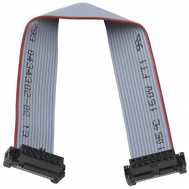
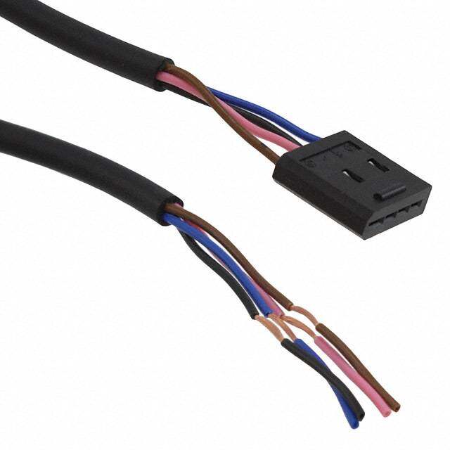
Platform Cable USB II System Suspend The cable's status LED is extinguished when the host system enters a suspend (power-saving) state. A system can suspend for a number of reasons. For example: (cid:129) The user puts the host system into standby or hibernate. (cid:129) The suspend function key on a laptop computer is pressed. (cid:129) The display panel of a laptop is closed. (cid:129) The host system is configured to suspend (standby or hibernate) after a specified amount of inactivity. The current drawn by the cable while suspended depends on the type of suspend state: standby or hibernate. While the host system is in standby, the cable draws approximately 350µA from the USB port. When the host is hibernating, all power is removed from the USB ports so the cable draws no current while in this state. The target interface output drivers are not powered while the host is suspended. These signals float to any DC bias level provided by the target hardware during suspend. If an iMPACT (10.1 or later) operation is in progress when suspend is attempted, iMPACT displays a message (Figure9) indicating that suspend is blocked until the operation is complete or manually aborted. Note: This feature is not supported in earlier versions of iMPACT, while iMPACT is operating in batch mode, or by other Xilinx design tools. In these cases, it is recommended that suspend be disabled in the host system when performing long, continuous operations. The cable is automatically disconnected when the host system is suspended. A reconnect is necessary when the host re- awakens from the suspend state (see Connecting to the Cable in iMPACT Software, page5). X-Ref Target - Figure 9 DS593_09_021408 Figure 9: Suspend Warning When iMPACT (10.1 or later) is Busy Platform Cable USB II Connections This section discusses physical connections from Platform Cable USB II to the host PC and the target system. High Performance Ribbon Cable A 6-inch ribbon cable is supplied and recommended for connection to target systems (Figure10). The cable incorporates multiple signal-ground pairs and facilitates error-free connections. The Xilinx product number for the 6-inch ribbon cable is HW-RIBBON14. To take advantage of the ribbon cable, a mating connector must be incorporated into the target system. This connector is normally installed only during prototype checkout. When the production hardware is functional and the ISP devices can be configured from alternate sources, the connector can be eliminated to reduce cost. Maintaining the footprint for this connector is recommended if space permits. DS593 (v1.5.1) August 6, 2018 www.xilinx.com 12
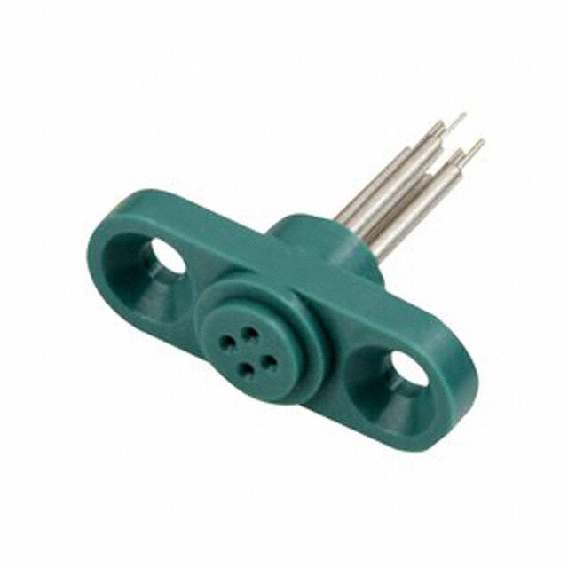
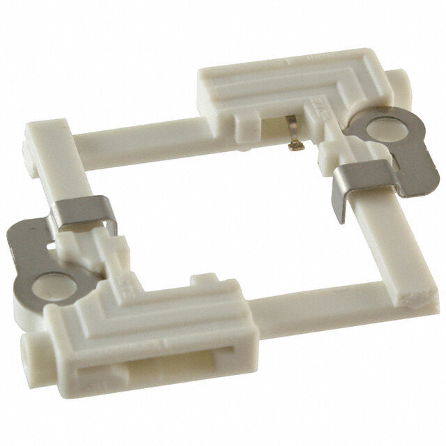
Platform Cable USB II The connector is a 2mm shrouded keyed header. See Table5, page15 for vendor part numbers and pin assignments. X-Ref Target - Figure 10 DS593_10_112607 Notes: 1. Ribbon Cable: 14-pin conductor, 1.0mm center, round-conductor flat cable, 28 AWG (7x36) stranded conductors, gray PVC with pin 1 edge marked. 2. 2mm ribbon female polarized connector, IDC connection to ribbon. Contacts are beryllium copper plated 30 micro-inches gold plating over 50-micro-inches nickel. The connectors mate to 0.5mm square posts on 2mm centers. Figure 10: High Performance Ribbon Cable Flying Wire Adapter An adapter with wires (Figure11) is provided for attachment to legacy target systems that do not incorporate a shrouded 2mm connector. The adapter makes it possible to use flying wires for connections to distributed terminals on a target system. The adapter is a small circuit board with two connectors (Figure12). The connector on the bottom side of the adapter mates with the 14-pin Platform Cable USB II male 2mm connector. A 7-pin right-angle header on the top side of the adapter mates with the standard Xilinx flying wire set. Note: This method of connection is not recommended because it can result in poor signal integrity. Additionally, damage can result if the leads are unintentionally connected to high voltages. The Xilinx product number for the flying wire set is HW-USB-FLYLEADS-G. X-Ref Target - Figure 11 RCooHmSpliant ® CON2NmEmCTOR STATUS Platform Cable USB II SIGNALS MPoowdeerl 5DVL C 1 00.15AHJTATA-LD-GT--IorSIeDN-rI-iIaNT--loMrOWS--SPP--II GGPGnnddND JTAG / SERIAL / SPI VRGENFD // GVNRDE F // GVNRDEF CERTIFIEDUHI-SSPEEBD MSaedrei ainl U .XS.UA. - 12345 VTTTRDMCE1OKS.F5 <PDCV RVORCORNELGEKEFFV M<SRI SC5SEO.KSF0 VDCGGG----nnnddd HTTACDTLKODT I // / / DC IDNOCIINLNTKE // // M WSMOCIPSSKIO TMS / PROG / SS ADAPTER DS593_11_021908 Figure 11: Flying Wire Adaptor (Top) with Wires DS593 (v1.5.1) August 6, 2018 www.xilinx.com 13
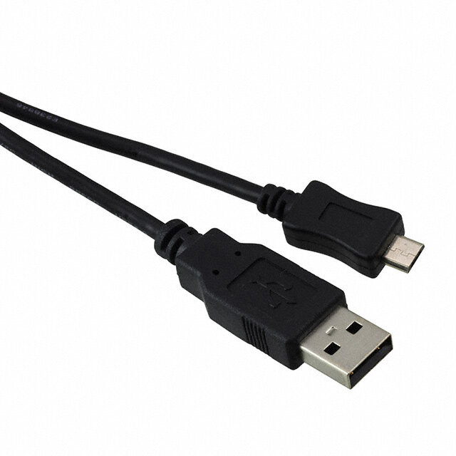
Platform Cable USB II X-Ref Target - Figure 12 Adapter Circuit Board DS593_12_012508 Figure 12: Flying Wire Adapter (Side) without Wires Physical Connection to the Host Each Platform Cable USB II includes a detachable, Hi-Speed-USB-certified, 1.8-meter A–B cable (Figure13). Under no circumstances should user-supplied cables exceed 5meters. Sub-channel cables (intended for low-speed 1.5Mb/s signaling) should not be used with Platform Cable USB II. A standard series B receptacle (Figure13) is incorporated into the case for mating with the detachable Hi-Speed A–B cable. A separate chassis ground is attached to the A–B cable drain wire and returns ESD current to the host system ground. X-Ref Target - Figure 13 DS593_13_112607 Figure 13: Standard A-B Host Interface Cable and Series B Receptacle DS593 (v1.5.1) August 6, 2018 www.xilinx.com 14
Platform Cable USB II Target Interface Connectors Mating connectors for attachment of the high-performance ribbon cable to a target system are available in both through-hole and surface mount configurations (Figure14). Shrouded and keyed versions should always be used to guarantee proper orientation when inserting the cable. The connector requires only 105mm2 of board space. The target system voltage applied to pin 2 of this connector is used as a power source for the output buffers that drive the output pins (see Target Interface Reference Voltage and Signals, page20). Table5, page15 provides some third-party sources for mating connectors that are compatible with the Platform Cable USBII ribbon cable. X-Ref Target - Figure 14 6.30 mm 7.59 mm 2.00 mm Slave 12.00 mm SPI Serial JTAG WP INIT HALT 14 13 PGND NC NC NC 12 11 GND 2.00 mm MOSI DIN TDI 10 9 GND TYP. MISO DONE TDO 8 7 GND 16.66 mm SCK CCLK TCK 6 5 GND SS PROG TMS 4 3 GND Vref Vref Vref 2 1 0.50 mm DS593_14_012508 Figure 14: Target Interface Connector Dimensions and Signal Assignments Table 5: Mating Connectors for 2mm pitch, 14-Conductor Ribbon Cable SMT, Through-Hole, Through-Hole, Manufacturer(1) Web Site Vertical Vertical Right Angle Molex 87832-1420 87831-1420 87833-1420 www.molex.com FCI 98424-G52-14 98414-G06-14 98464-G61-14 www.fciconnect.com Comm Con Connectors 2475-14G2 2422-14G2 2401R-G2-14 www.commcon.com Notes: 1. Some manufacturer pin assignments do not conform to Xilinx pin assignments. Please refer to the manufacturer’s data sheet for more information. 2. Additional ribbon cables can be purchased separately from the Xilinx Online Store. DS593 (v1.5.1) August 6, 2018 www.xilinx.com 15
Platform Cable USB II Target System Connections This section provides examples of the various configuration topologies supported by Platform Cable USB II. Each example incorporates the 2mm connector (see Target Interface Connectors, page15) as the cable interface. Diagrams in this section provide a functional relationship between the cable interface and the target devices. Note: Signal integrity is not considered in these examples. Refer to Signal Integrity, page28 for details on buffering and termination. JTAG and Slave Serial Multiple devices can be cascaded when using either a JTAG or slave-serial topology in target systems. Figure15 and Figure17, page18 show typical routing for JTAG and slave-serial topologies, respectively. Note: The cable supports the slave-serial topology with iMPACT v10.1 only. The Vivado Design Tools do not support slave-serial with the cable. Platform Cable USB II provides a multi-use signal on its target interface connector called pseudo ground (PGND). The PGND pin is connected to an open-drain driver (see Pseudo Ground Signal in iMPACT, page23); hence, it is either Low or high-Z. The behavior of PGND is determined by the host application connected to the cable. In iMPACT, PGND is active-Low during JTAG, slave-serial and SPI operations (for example, programming, configuration, read back, etc.) and high-Z when the cable is idle. Figure16, page17 shows a typical use of PGND as a control signal to manage a target system’s JTAG chain. PGND drives the select (S) term on a set of multiplexers that switch between the primary configuration source and the cable. When PGND is active-Low, the cable drives the JTAG chain. When PGND is high-Z, the primary configuration source drives the JTAG chain. This capability allows Platform Cable USB II to remain attached to the target system while remaining isolated from the primary configuration source. A similar scheme can be used with slave-serial topologies. Note: PGND is supported in Vivado Hardware Manager and Xilinx SDK tools. These tools drive PGND Low while the application is connected to the cable. PGND is high-Z when all applications are disconnected from the cable. Note: PGND is supported in iMPACT versions 10.1 and later. PGND remains high-Z in earlier versions of iMPACT and in Xilinx design tools that do not support PGND. The DONE pin on FPGAs can be programmed to be an open-drain or active driver. For cascaded slave-serial topologies, an external pull-up resistor should be used, and all devices should be programmed for open-drain operation. X-Ref Target - Figure 15 2-mm Connector VCCAUX(1) VREF 2 TDO 8 ISP FPGA CPLD TDI 10 TDI PROM TDO TDI TDO TDI TDO TMS 4 TMS TCK TMS TCK TMS TCK TCK 6 GND(2) * DS593_15_011508 Notes: 1. Example implies that V , V , and V for various devices are set to the same voltage. Refer to the device data sheet for the CCO CCJ CCAUX appropriate JTAG voltage-supply levels. 2. Attach the following 2mm connector pins to digital ground: 3, 5, 7, 9, and 11. Figure 15: Example of JTAG Chain Topology DS593 (v1.5.1) August 6, 2018 www.xilinx.com 16
Platform Cable USB II X-Ref Target - Figure 16 V CCAUX 1 1 1 0 0 0 K K K Ω Ω Ω e urc TDO JTAG CHAIN o (4) on Sary) TDI A Y uratiPrim TMS B TDI TDO g( nfi S Co TCK TMS TCK (4) A Y V (1) 2-mm CCAUX B Connector S (4) A V 2 REF Y B TDO 8 B II S S e Uary) TDI 10 VCCAUX bld an TMS 4 Co MUX Truth Table orm (Sec TCK 6 PRuellq-Uuipre(3d) 1 KΩ S Output atf H Y = A PlPGND(5) 13 L Y = B GND(2) * DS593_16_021408 Notes: 1. Example implies that V , V , and/or V for various devices in the JTAG chain are set to the same voltage. CCO CCJ CCAUX 2. Attach the following 2mm connector pins to digital ground: 3, 5, 7, 9, and 11. 3. The cable uses an open-drain driver to control the pseudo ground (PGND) signal — an external pull-up resistor is required. 4. Assumes that the multiplexor supply voltages pins are connected to V . CCAUX 5. Pin 13 is grounded on legacy Xilinx USB cables (models DLC9, DLC9G and DLC9LP), and Parallel Cable IV (model DLC7). These cables need to be manually detached from the 2mm connector to allow the primary configuration source to have access to the JTAG chain. Figure 16: Example Using PGND in a JTAG Chain with the ISE iMPACT Tool DS593 (v1.5.1) August 6, 2018 www.xilinx.com 17
Platform Cable USB II Direct SPI Platform Cable USB II can connect directly to a single SPI flash device. Figure18, page19 shows an example SPI flash connection. The application note Configuring Xilinx FPGAs with SPI Serial Flash (XAPP951) provides additional details of the cable connections necessary to program a FPGA bitstream into a SPI flash device. Note: See Configuring Xilinx FPGAs with SPI Serial Flash for a list of supported SPI devices. Direct SPI is supported with iMPACT v10.1 only. The Vivado Design Tools do not support direct SPI with the cable. By connecting PGND to PROG_B of the FPGA (Figure17), the FPGA can be commanded to set its SPI signals to high-Z while the cable programs a SPI flash device. PGND is pulled Low when the cable is driving its SPI signals in SPI mode and set to high-Z when the cable is not driving its SPI signals. PGND eliminates the need for a hardware jumper to ground on the PROG_B signal and the need for additional control logic. PGND is controlled by an open-drain driver. Note: PGND control for SPI programming is available in iMPACT versions 9.2i and later. X-Ref Target - Figure 17 VCCAUX(2) 2-mm Connector 470Ω(4) VCCAUX(2) VREF 2 DONE 8 PROG DONE PROG DONE PROG DONE PROG 4 DIN 10 DIN FPGA1 DOUT DIN FPGA2 DOUT DIN FPGAn DOUT INIT 14 VCCO(2) INIT CCLK(1) INIT CCLK(1) INIT CCLK(1) CCLK 6 GND(3) * DS593_17_021408 Notes: 1. Set mode pins (M2-M0) on each FPGA to slave-serial mode when using the USB cable, so the CCLK is treated as an input. 2. Example uses generalized nomenclature for the voltages-supply levels. Refer to the device data sheet for the appropriate serial configuration voltage-supply levels. 3. Attach the following 2mm connector pins to digital ground: 3, 5, 7, 9, and 11. 4. A pull-up is required when two or more devices are cascaded and programmed for open-drain operation. 5. This diagram is not applicable to the Vivado Design Tools. The Vivado Design Tools do not support the slave-serial topology. Figure 17: Example of Cascaded Slave-Serial Topology with the iMPACT Software DS593 (v1.5.1) August 6, 2018 www.xilinx.com 18
Platform Cable USB II X-Ref Target - Figure 18 + 3.3V 2 mm Connector 2 V REF 8 MISO 10 MOSI 4 SS 6 SCK 13 PGND * GND(4) +2.5V +3.3V +1.2V +3.3V V V V V C C C C C C C C AUX O_2 O_0 INT VCC MOSI D W ‘1’ DIN SPI Bus(5) Q ST Micro Spartan-3E(2) M25Pxx(1) FPGA SPI Flash CSO_B S HOLD ‘1’ CCLK C + 2.5V GND Ω(3) k 7 4. GND PROG_B DS593_18_021508 Notes: 1. The pin names for a ST Microsystems M25Pxx serial flash device are shown in this example. SPI flash devices from other vendors can have different pin names and requirements. Refer to the SPI flash data sheet for the equivalent pins and device requirements. 2. The example shows the interconnect and device requirements for a Xilinx Spartan-3E FPGA. Other SPI-capable FPGAs can have different pin names and requirements. Please refer to the FPGA data sheet for equivalent pins and device requirements. 3. The cable uses an open-drain driver to control the pseudo ground (PGND) signal — an external pull-up resistor is required. 4. Attach the following 2mm connector pins to digital ground: 3, 5, 7, 9 and 11. 5. Typically, an FPGA and other slave SPI devices (not shown) are connected to the SPI bus. The other devices on the SPI bus must be disabled when the cable is connected to the 2mm connector to avoid signal contention. When a Xilinx FPGA is connected to the SPI bus, the cable holds the FPGA PROG_B pin Low to insure the FPGA SPI pins are 3-stated. 6. This diagram is not applicable to the Vivado Design Tools. The Vivado Design Tools do not support the direct SPI topology. Figure 18: Example of Direct SPI Topology with the iMPACT Software Indirect SPI When used with Xilinx design tools, Platform Cable USB II can be used to indirectly program some third-party SPI serial flash PROMs via the target FPGA's JTAG port. For a complete description on using Platform Cable USB II for indirect programming of third-party SPI serial flash PROMs and for a complete list of supported SPI serial flash memories, refer to the application note Indirect Programming of SPI Serial Flash PROMs with Spartan-3A FPGAs (XAPP974). DS593 (v1.5.1) August 6, 2018 www.xilinx.com 19
Platform Cable USB II Indirect BPI When used with the ISE design tools, Platform Cable USB II can be used to indirectly program Platform Flash XL, or some third-party NOR flash memories (BPI PROMs) via the target FPGA's JTAG port. For a description of the indirect Platform Flash programming solution, see the Platform Flash XL User Guide (UG438). For a complete description on using Platform Cable USB II for indirect programming of third-BPI PROMs and for a complete list of supported BPI PROMs, refer to the iMPACT Flash device support table. Target Interface Reference Voltage and Signals Target Reference Voltage Sensing (V ) REF Platform Cable USB II incorporates an over-voltage clamp on the V pin of the 2mm ribbon cable connector. The clamped REF voltage (V ) supplies high-slew-rate buffers that drive each of the output signals (see Output Driver Structure). REF_CLAMP V must be a regulated voltage. REF Note: Do not insert a current-limiting resistor in the target system between the V supply and pin 2 on the 2mm connector. REF When Platform Cable USB II is idle, a nominal amount of current is drawn from the target system V . Figure19 shows the REF V current as a function of V voltage. REF REF No damage to Platform Cable USB II occurs if the A–B cable is unplugged from the host while the ribbon cable or flying leads are attached to a powered target system. Similarly, no damage to target systems occurs if Platform Cable USB II is powered and attached to the target system while the target system power is off. Bidirectional Signal Pins Platform Cable USB II provides five bidirectional signal pins: TDI_DIN_MOSI, TDO_DONE_MISO, TCK_CCLK_SCK, TMS_PROG_SS and HALT_INT_WP. Each pin incorporates the same I/O structure. The state of each pin (reading or writing) is determined by the current mode of the cable (JTAG, SPI, or slave-serial). Output Driver Structure Each output signal is routed through a NC7SZ126 ultra high-speed CMOS buffer (Figure20, page21). Series-damping resistors (30.1Ω) reduce reflections. Weak pull-up resistors (20kΩ) terminating at V maintain a defined logic level REF_CLAMP when the buffers are set to high-Z. Schottky diodes provide the output buffers with undershoot protection. The FPGA sets the output buffers to high-Z when V drops below 1.30 V. In addition, an over-voltage Zener on V REF REF clamps V to approximately 3.9V. REF_CLAMP Figure21, page22 shows the relationship between the output drive voltage and V . REF Note: The output drivers are enabled only during cable operations; otherwise, they are set to high-Z between operations. Xilinx design tools actively drive the outputs to logic 1 before setting the respective buffer to high-Z, avoiding the possibility of a slow rise-time transition caused by a charge path through the pull-up resistor into parasitic capacitance on the target system. DS593 (v1.5.1) August 6, 2018 www.xilinx.com 20
Platform Cable USB II X-Ref Target - Figure 19 DS593_19_021408 Figure 19: V Current vs. V Voltage REF REF X-Ref Target - Figure 20 V REF_CLAMP Ω FPGA NC7SZ126 V 20 k REF_CLAMP 2-mm Connector Output 30.1Ω I/O Pin High-Z Control BAT54 To input buffer DS593_20_021408 Figure 20: Target Interface Driver Topology DS593 (v1.5.1) August 6, 2018 www.xilinx.com 21
Platform Cable USB II X-Ref Target - Figure 21 ) V ( e g a olt V e v ri D ut p ut O V Voltage (VDC) REF DS593_21_021408 Figure 21: Output Drive Voltage vs. V REF Input Receive Structure Figure22 shows the input receive structure. Each input signal is routed through a NC7WZ07 ultra high-speed CMOS, open- drain receive buffer. Series-termination resistors (499Ω) provide current limit protection for positive and negative excursions. Schottky diodes provide the input buffers with undershoot protection. The receive buffers are biased by an internal 1.8V power supply. See Table9, page33 for V and V specifications. The receive buffers can tolerate voltages higher than the IL IH bias voltage without damage, compensating for target system drivers in multi-device chains where the last device in the chain might be referenced to a voltage other than V (for example, the TDO output at the end of a JTAG chain). REF X-Ref Target - Figure 22 To output buffer FPGA NC7WZ07 2 mm Connector Input 499Ω I/O Pin BAT54 DS593_22_021408 Figure 22: Target Interface Receiver Topology DS593 (v1.5.1) August 6, 2018 www.xilinx.com 22
Platform Cable USB II Pseudo Ground Signal in iMPACT The pseudo ground (PGND) pin on target interface connector is routed to a ultra-high-speed buffer with an open-drain output (Figure23). A pull-up resistor is required on target systems that utilize this signal. The buffer can tolerate a pull-up voltage as high as 6.0V. X-Ref Target - Figure 23 FPGA NC7WZ07 2-mm Connector PGND_CNTL A Y PGND Input Output A Y H Z L L DS593_23_021508 Figure 23: PGND Signal HALT_INIT_WP Signal in iMPACT Platform Cable USB II provides a second multi-use signal on its target interface connector called HALT_INIT_WP (this signal is referred to as HALT when the cable is in JTAG mode). The HALT_INIT_WP pin is connected to a three-state CMOS driver (see Bidirectional Signal Pins, page20). The behavior of HALT_INIT_WP is determined by the host application connected to the cable. iMPACT provides the option of enabling the HALT pin during JTAG operations (Figure24). This option is accessed by clicking on the Xilinx FPGA in the iMPACT GUI and selecting Edit → Set Programming Properties… to open the Device Programming Properties dialog box. Check “Assert Cable INIT during programming” to enable the HALT signal. When enabled in iMPACT, HALT is active-Low while the cable is performing JTAG operations on any Xilinx FPGA and high- Z when the cable is idle. HALT is active-High while JTAG operations are being performed on other devices. The HALT signal remains high-Z when not enabled (iMPACT default) or when the cable is in slave-serial or SPI modes. Note: HALT signal control is available in iMPACT 9.2i and later. The Vivado Design Tools do not support the HALT function. HALT remains high-Z in earlier versions of iMPACT and in Xilinx design tools where the HALT signal is not supported. DS593 (v1.5.1) August 6, 2018 www.xilinx.com 23
Platform Cable USB II X-Ref Target - Figure 24 DS593_24_021408 Figure 24: Enabling the HALT Signal in iMPACT (9.2i) Timing Specifications For JTAG, SPI, and slave-serial configuration modes, the TDI_DIN_MOSI and TMS_PROG_SS outputs change on falling edges of TCK_CCLK_SCK (Figure25). Target devices sample TDI_DIN_MOSI and TMS_PROG_SS on rising edges of TCK_CCLK_SCK. The minimum setup time T for target device sampling of TDI_DIN_MOSI or TMS_PROG_SS is: TSU(MIN) T = T – T TSU(MIN) CLK/2 CPD(MAX) = 20.8ns – 16.0ns = 4.8ns where: T = TCK_CCLK_SCK low time at 24MHz, CLK/2 T = Maximum TDI_DIN_MOSI or TMS_PROG_SS propagation delay relative to TCK_CCLK_SCK inherent in CPD(MAX) the output stage of the cable. Reducing the TCK_CCLK_SCK frequency increases the data setup time at the target. Note: Timing specifications apply when V = 3.3V. Operations at 24MHz might not be possible when using a V below 3.3V due to REF REF the increased propagation delay through the output buffer stage of the cable. TDO/MISO Timing Considerations Designers of target systems must take care to observe specific timing requirements for TDO (JTAG chains) or MISO (dedicated SPI in-system programming) when incorporating the 2mm IDC connector. In particular, if an open-drain or open- collector buffer is inserted between TDO (MISO) and the cable, the value of the pull-up resistor at the output of such buffers must be relatively small (for example, less than 330Ω) to avoid delays associated with parasitic capacitance. Figure26, page26 and Figure27, page27 show the timing relationship between TCK and TDO. The signal TDO_SMPL is an internal logic signal not available at the target interface, but is shown to highlight the location of the TDO sampling point. In Figure26, the negative TCK transition at G1 causes the last device in the target system JTAG chain to drive TDO, which propagates to the cable at G2. The time from G1 to G2 is the sum of the propagation delays in the driver stage of the target device and the receiver stage of the cable (37ns in this example). In Figure27, the cursors show the total setup time (42ns) before TDO is sampled by the cable. Figure28, page28 is an analog representation of the logical condition shown in Figure26 and Figure27 captured at the target system. DS593 (v1.5.1) August 6, 2018 www.xilinx.com 24
Platform Cable USB II Note: The propagation delay from TCK to TDO is 26ns. Because Figure26 shows a propagation delay of 37ns, the difference of 11ns is attributable exclusively to input delays in the cable. At 12MHz, there is still sufficient setup time before the cable samples prior to the next negative TCK transition. X-Ref Target - Figure 25 TMS_PROG changes on Negative TDI_DIN Changes Edge of TCK_CCLK (G1) on Negative Edge of TCK_CCLK (G2) DS593_25_021408 Figure 25: TDI_DIN_MOSI and TMS_PROG_SS Timing with Respect to TCK_CCLK_SCK DS593 (v1.5.1) August 6, 2018 www.xilinx.com 25
Platform Cable USB II X-Ref Target - Figure 26 Negative TCK transition at G1 causes target device to change TDO state, which propagates to the cable at G2 in less than ½ clock cycle in this 12-MHz example. DS593_26_021408 Figure 26: TDO Sampling Example at 12MHz (TDO Propagation Delay) DS593 (v1.5.1) August 6, 2018 www.xilinx.com 26
Platform Cable USB II X-Ref Target - Figure 27 TDO setup time prior to internal sampling clock (G2 – G1) is 42ns in this 12-MHz example. DS593_27_011508 Figure 27: TDO Sampling Example at 12MHz (TDO Setup Time Relative to Sampling Point) DS593 (v1.5.1) August 6, 2018 www.xilinx.com 27
Platform Cable USB II X-Ref Target - Figure 28 Propagation delay from A to B (26 ns) captured directly at the target represents 70% of the total propagation delay seen by the cable (Figure 25). TDO Sampling Point TCK TDO TDO Sampling Point DS593_28_021408 Figure 28: TDO Sampling Example at 12MHz (Analog Signals on Target System) Signal Integrity Platform Cable USB II uses high-slew-rate buffers to drive its output pins. Each buffer has a 30.1Ω series termination resistor. Users should pay close attention to PCB layout to avoid transmission line effects. Visit the Xilinx Signal Integrity Central website for detailed signal integrity assistance. If the target system has only one programmable device, the 2mm connector should be located as close as possible to the target device. If there are multiple devices in a JTAG or slave-serial single chain on the target system, users should consider buffering TCK_CCLK_SCK. Differential driver/receiver pairs provide excellent signal quality when the rules identified in Figure29 are followed. Buffering is essential if target devices are distributed over a large PCB area. X-Ref Target - Figure 29 Route A & B traces for each differential SN65LVDS105 pair in parallel with equal length and Four Differential consistent spacing Drivers SN65LVDS2 (2) Series Termination Resistor (20Ω −30Ω) TCK_CCLK_SCK 1 TCK_CCLK_SCK1 Four Buffered Clocks 4 TCK_CCLK_SCK4 Locate one receiver adacent to each target device Locate driver package adjacent to 2-mm connector DS593_29_021408 Figure 29: Differential Clock Buffer Example Each differential driver and/or receiver pair contributes approximately 5ns of propagation delay. This delay is insignificant when using 12MHz or slower clock speeds. DS593 (v1.5.1) August 6, 2018 www.xilinx.com 28
Platform Cable USB II Each differential receiver can drive multiple target devices if there are no branches on the PCB trace and the total trace length is less than four inches. A series termination resistor should be placed adjacent to the single-ended output of the differential receiver. Note: If the target chain has, for example, a JTAG or slave-serial topology and a 24MHz clock rate is desired, it is recommended that matching buffers be used for both TCK_CCLK_SCK and TMS_PROG_SS. Matching buffers maintains a consistent phase relationship between TCK_CCLK_SCK and TMS_PROG_SS. A buffer is not needed for TDI_DIN_MOSI, because it sees only one load. USB Hub Types and Cable Performance There are two important hub specifications affecting the performance of Platform Cable USB II: maximum port current and total bandwidth. Maximum Port Current Platform Cable USB II is a bus-powered device, drawing less than 150mA from the host USB port under all operating conditions. Note: Some older USB root hubs or external bus-powered hubs might restrict peripherals to 100mA. Platform Cable USB II cannot enumerate on hubs with the 100mA restriction. Total Bandwidth The maximum theoretical bandwidth is 480Mb/s for a single USB 2.0 Hi-Speed device and 12Mb/s for a single USB 1.1 full- speed device. However, because hub bandwidth must be shared among all connected devices, actual bandwidth is in practice lower than these theoretical values. Platform Cable USB II performance is optimal when enumerated on a USB 2.0 Hi-Speed port. Hi-Speed USB operation is guaranteed only if the cable is attached directly to a USB 2.0 root hub (Figure30E), or to an external, self-powered USB 2.0 hub connected directly to a USB 2.0 root hub (Figure30D). If Platform Cable USB II is attached to a USB 1.1 root hub (Figure30A) or to USB 2.0 external hub connected to a USB 1.1 root hub (Figure30B), the cable enumerates as a full-speed device and cable performance is degraded. Communication and protocol overhead limits any given USB device to approximately 30% of total bandwidth. For USB 1.1 hubs, the maximum achievable throughput is approximately 3.6Mb/s. Certain self-powered, USB 2.0 hubs can continue to function as USB 1.1 hubs when disconnected from their external power source (Figure30C). When no external power source is present, these hubs draw their power from their upstream USB port. If Platform Cable USB II is connected to such a hub while operating at USB 1.1 speeds, the cable enumerates as a full- speed device. Furthermore, bus-powered hubs can only deliver a total of 500mA to all connected devices. If individual ports on bus-powered hubs are limited to less than 150mA, Platform Cable USB II does not enumerate and is unavailable for use by host software applications. DS593 (v1.5.1) August 6, 2018 www.xilinx.com 29
Platform Cable USB II X-Ref Target - Figure 30 (A) (B) (C) (D) (E) 12 Mb/s Bus Speed 12 Mb/s Bus Speed 480 Mb/s Bus Speed 480 Mb/s Bus Speed 480 Mb/s Bus Speed 1.X Root Hub 1.X Root Hub 2.0 Root Hub 2.0 Root Hub 2.0 Root Hub 500 500 500 500 500 mA mA mA mA mA Power Power 2.0 External 2.0 External 2.0 External Platform Cable Platform Cable Bus-Powered Self-Powered Self-Powered USB II USB II Hub Hub Hub Enumerates at Enumerates at full speed because < 500 < 500 500 Hi-Speed — best root hub only mA mA mA performance due to operates at full high bus speed. speed — degraded performance due to slow bus speed Platform Cable Platform Cable Platform Cable USB II USB II USB II Enumerates at Enumerates at full speed Enumerates at full speed because because 2.0 external Hi-Speed — best root hub only hub operates at full performance due to operates at full speed — degraded high bus speed. speed — degraded performance due to slow performance due bus speed. Cable may to slow bus speed not enumerate. DS593_30_021408 Figure 30: Platform Cable USB II Performance with Various Hub Types Interface Pin Descriptions Table 6: JTAG/SPI/Slave Serial Port: 2mm Connector Signals MODE Pin Direction(2) Description Number JTAG SPI Slave-Serial Configuration Programming(1) Configuration Target Reference Voltage(3). This pin should be connected to a voltage bus on the target system that serves the JTAG, SPI, or 2 V V V In slave-serial interface. For example, when REF REF REF programming a CoolRunner-II device using JTAG, V should be connected to the REF target V bus. AUX JTAG Test Mode Select. This pin is the JTAG mode signal establishing appropriate 4 TMS – – Out TAP state transitions for target ISP devices sharing the same data stream. JTAG Test Clock. This pin is the clock signal for JTAG operations and should be 6 TCK – – Out connected to the TCK pin on all target ISP devices sharing the same data stream. JTAG Test Data Out. This pin is the serial 8 TDO – – In data stream received from the TDO pin on the last device in a JTAG chain. DS593 (v1.5.1) August 6, 2018 www.xilinx.com 30
Platform Cable USB II Table 6: JTAG/SPI/Slave Serial Port: 2mm Connector Signals (Cont’d) MODE Pin Direction(2) Description Number JTAG SPI Slave-Serial Configuration Programming(1) Configuration JTAG Test Data In. This pin outputs the 10 TDI – – Out serial data stream transmitted to the TDI pin on the first device in a JTAG chain. JTAG Pseudo Ground. Use of this pin is optional. PGND is pulled Low during JTAG operations; otherwise, it is high-Z. This pin is 13 PGND – – Out connected to an open-drain driver and requires a pull-up resistor on the target system.(4) JTAG Halt. Use of this pin is optional. Host applications can customize the behavior of 14 HALT – – Out this signal. See HALT_INIT_WP Signal in iMPACT, page23. SPI Select. This pin is the active-Low SPI 4 – SS – Out chip select signal and should be connected to the S(1) pin on the SPI flash device. SPI Clock. This pin is the clock signal for 6 – SCK – Out SPI operations and should be connected to the C(1) pin on the SPI flash PROM. SPI Master-Input, Slave-Output. This pin is the target serial output data stream and 8 – MISO – In should be connected to the Q(1) pin on the SPI flash device. SPI Master-Output Slave-Input. This pin outputs the target serial input data stream 10 – MOSI – Out for SPI operations and should be connected to the D(1) pin on the SPI flash device. SPI Pseudo Ground. PGND is pulled Low during SPI operations; otherwise, it is high- Z. When connected to PROG_B on an FPGA, the FPGA will high-Z its SPI signals 13 – PGND – Out while the cable is programming the SPI flash. This pin is connected to an open-drain driver and requires a pull-up resistor on the target system.(4) SPI Write Protect. This pin is reserved for 14 – WP – – future use. Do not connect for SPI programming. Slave Serial Configuration Reset. This pin is used to force a reconfiguration of the target FPGA(s) and should be connected to 4 – – PROG Out the PROG_B pin of the target FPGA for a single-device system, or to the PROG_B pin of all FPGAs in parallel in a daisy-chain configuration. Slave Serial Configuration Clock. FPGAs load one configuration bit per CCLK cycle in slave-serial mode. CCLK should be 6 – – CCLK Out connected to the CCLK pin on the target FPGA for single-device configuration, or to the CCLK pin of all FPGAs in parallel in a daisy-chain configuration. DS593 (v1.5.1) August 6, 2018 www.xilinx.com 31
Platform Cable USB II Table 6: JTAG/SPI/Slave Serial Port: 2mm Connector Signals (Cont’d) MODE Pin Direction(2) Description Number JTAG SPI Slave-Serial Configuration Programming(1) Configuration Slave Serial Configuration Done. This pin indicates to Platform Cable USB II that target FPGAs have received the entire configuration bitstream and should be 8 – – Done In connected to the Done pin on all FPGAs in parallel for daisy-chained configurations. Additional CCLK cycles are issued following the positive transition of Done to insure that the configuration process is complete. Slave Serial Configuration Data Input. This pin outputs the serial input data stream for target FPGAs and should be connected 10 – – DIN Out to the DIN pin of the target FPGA in a single- device system, or to the DIN pin of the first FPGA in a daisy-chain configuration. Slave Serial Pseudo Ground. Use of this pin is optional. PGND is pulled Low during slave-serial operations; otherwise, it is high- 13 – – PGND Out Z. This pin is connected to an open-drain driver and requires a pull-up resistor on the target system.(4) Slave Serial Configuration Initialization. This pin indicates that configuration memory is being cleared and should be connected to 14 – – INIT In the INIT_B pin of the target FPGA for a single-device system, or to the INIT_B pin on all FPGAs in parallel in a daisy-chain configuration. Digital Ground. All ground pins should be 3, 5, 7, 9, – – – – connected to digital ground on the target 11 system to minimize crosstalk. 1, 12 – – – – Not Connected. Notes: 1. The listed SPI pin names match those of SPI flash devices from ST Microelectronics. Pin names of compatible SPI devices from other vendors can vary. Consult the vendor's SPI device data sheet for equivalent pin names. 2. The signal pins (HALT_INIT_WP, TDI_DIN_MOSI, TDO_DONE_MISO, TCK_CCLK_SCK, TMS_PROG_SS) are bidirectional. Their directions during cable operations are defined by the current configuration or programming mode (JTAG, SPI, or slave-serial). 3. The target reference voltage must be regulated and not have a current-limiting resistor in series with the V pin. REF 4. For more details, see Target System Connections, page16 and Pseudo Ground Signal in iMPACT, page23. Platform Cable USB II Operating Characteristics Table 7: Absolute Maximum Ratings(1) Symbol Description Conditions Value Units V USB Port Supply Voltage 5.25 V BUS V Target Reference Voltage 6.00 V REF I Target Supply Current V = 5.25V 100 mA REF REF ° T Ambient Operating Temperature 70 C A DS593 (v1.5.1) August 6, 2018 www.xilinx.com 32
Platform Cable USB II Table 7: Absolute Maximum Ratings(1) (Cont’d) Symbol Description Conditions Value Units DC Output Current (TCK_CCLK_SCK, I TMS_PROG_SS, TDI_DIN_MOSI, and ±24 ±mA OUT INIT) Notes: 1. Exposure to absolute rating conditions for extended periods of time can affect product reliability. The values listed in this table are stress ratings only. Functional operation of the product at these or any other conditions beyond those listed under Table8: Recommended DC Operating Conditions is not implied or recommended. Table 8: Recommended DC Operating Conditions Symbol Description Conditions Min Max Units V USB Port Supply Voltage 4.00 5.25 V BUS V Target Reference Voltage 1.5 5.00 V REF T Ambient Operating Temperature 0 70 oC A T Storage Temperature –40 +85 oC STG Table 9: DC Electrical Characteristics Symbol Description Conditions Min Max Units V = 3.3V 15 REF V = 2.5V 3 REF I Target Supply Current mA REF V = 1.8V 1 REF V = 1.5V 1 REF V = 3.3V; I = –8mA 2.25 REF OH V = 2.5V; I = –8mA 2.15 REF OH V High-Level Output Voltage V OH V = 1.8V; I = –8mA 1.55 REF OH V = 1.5V; I = –8mA 1.30 REF OH V = 3.3V; I = 16mA 0.40 REF OH V Low-Level Output Voltage V = 2.5V; I = 8mA 0.30 V OL REF OH V = 1.5V; I = 4mA 0.24 REF OH V High-Level Input Voltage V = 1.5V to 3.3V 1.35 V IH REF V Low-Level Input Voltage V = 1.5V to 3.3V 0.45 V IL REF I Dynamic Current(1) V = 5.25V: TCK = 24MHz 85 110 mA CC1 BUS I Dynamic Current(2) V = 5.25V; TCK = 6MHz 85 100 mA CC2 BUS I Suspend Current V = 5.25V 250 350 μA CCSU BUS Notes: 1. Operating at Hi-Speed on a USB 2.0 port. 2. Operating at full-speed on a USB 1.1 port. Table 10: Switching Characteristics Symbol Description Conditions Min Max Units T Clock Period 750kHz 1333 ns CLK TCK 24MHz 41.66 ns T Cable Propagation Delay Time CPD (TDI or TMS relative to the negative V = 1.5V to 3.3V 16 ns REF edge of TCK) DS593 (v1.5.1) August 6, 2018 www.xilinx.com 33
Platform Cable USB II Table 10: Switching Characteristics (Cont’d) Symbol Description Conditions Min Max Units T Target Setup Time TSU (TDI or TMS relative to the V = 1.5V to 3.3V 4.8 ns REF positive edge of TCK) T Cable Setup Time CSU (TDO relative to the V = 1.5V to 3.3V 15.8 ns REF negative edge of TCK) T Target Propagation Delay Time TPD (TDO relative to the V = 1.5V to 3.3V 24.6 ns REF negative edge of TCK) X-Ref Target - Figure 31 Target devices samples TMS_PROG_SS and TDI_DIN_MOSI on the rising edge of TCK_CCLK_SCK Target device asserts TDO_DONE_MISO on the falling edge of TCK_CCLK_SCK T CLK T TSU TCK_CCLK_SCK T CPD TMS_PROG_SS / TDI_DIN_MOSI Platform Cable USB II asserts TMS_PROG_SS and TTPD TDI_DIN_MOSI on the falling T edge of TCK_CCLK_SCK CSU TDO_DONE_MISO Platform Cable USB II samples TDO_DONE_MISO on the falling edge of TCK_CCLK_SCK DS593_31_021408 Notes: 1. All times are in nanoseconds and are relative to the target system interface connector. 2. T Min is the minimum setup time guaranteed by Platform Cable USB II relative to the positive edge of TCK_CCLK_SCK. TSU 3. T Min is the minimum setup required by Platform Cable USB II to properly sample TDO_DONE_MISO. CSU 4. Propagation delays associated with buffers on the target system must be taken into account to satisfy the minimum setup times. Figure 31: Platform Cable USB II Timing Diagram USB-IF Compliance Platform Cable USB II is certified by the USB Integrators Forum (USB-IF). Certification is achieved when a product passes a battery of tests required by the USB-IF Compliance Program. These tests (performed at an independent test facility) measure a product's conformity with Universal Serial Bus Specification Revision 2.0 and establish a reasonable level of DS593 (v1.5.1) August 6, 2018 www.xilinx.com 34
Platform Cable USB II acceptability. Products that pass this level of acceptability are added to the USB-IF Integrator's List and receive the rights of usage for the USB logo. FCC Notice This equipment has been tested and found to comply with the limits for a Class A digital device, pursuant to Part 15 of the FCC Rules. These limits are designed to provide reasonable protection against harmful interference when the equipment is operated in a commercial environment. This equipment generates, uses, and can radiate radio frequency energy and, if not installed and used in accordance with the data sheet, could cause harmful interference to radio communications. Operation of this equipment in a residential area is likely to cause harmful interference, in which case, the user is required to correct the interference at his own expense. Industry Canada Information This Class A digital apparatus complies with Canadian ICES-003. Ordering Information Platform Cable USB II ships with each of the items shown in Table11 plus a 1.8-meter, Hi-Speed USB, A-B cable. Table 11: Ordering Information Item Product Number Platform Cable USB II HW-USB-II-G Ribbon Cable, 6-inch HW-RIBBON14 Flying Wire Set HW-USB-FLYLEADS-G Marking Information Table 12: Marking Information Model Name Serial Prefix Description DLC10 XU Platform Cable USB II DS593 (v1.5.1) August 6, 2018 www.xilinx.com 35
Platform Cable USB II Revision History The following table shows the revision history for this document: Date Version Description of Revisions 03/03/2008 1.0 Initial Xilinx release. 05/14/2008 1.1 (cid:129) Updated trademark references. (cid:129) Added support for Platform Flash XL. 06/09/2008 1.2 Corrected the functional descriptions of pins 6 and 8 in Table6, page30. 03/17/2011 1.2.1 Converted document to latest template containing current Xilinx logos and colors. 06/25/2014 1.3 Updated support information for Xilinx tools and added references to the Vivado Design Suite throughout the data sheet. Updated the devices listed in Table3. Updated the Notice of Disclaimer. 01/16/2015 1.4 Updated note for 24MHz in Table2. Updated notes about PGND in JTAG and Slave Serial. Removed obsolete XC4000, XC9500, XC9500XV, and Spartan devices from Features, Table3, and Signal Integrity. 06/23/2015 1.5 In Figure16, removed note 6 about the Vivado tools not supporting the cable PGND signal. In Pseudo Ground Signal in iMPACT, removed sentences stating that the Vivado tools do not support the PGND function. 08/06/2018 1.5.1 Editorial updates only. No technical content updates. Notice of Disclaimer The information disclosed to you hereunder (the “Materials”) is provided solely for the selection and use of Xilinx products. To the maximum extent permitted by applicable law: (1) Materials are made available "AS IS" and with all faults, Xilinx hereby DISCLAIMS ALL WARRANTIES AND CONDITIONS, EXPRESS, IMPLIED, OR STATUTORY, INCLUDING BUT NOT LIMITED TO WARRANTIES OF MERCHANTABILITY, NON-INFRINGEMENT, OR FITNESS FOR ANY PARTICULAR PURPOSE; and (2) Xilinx shall not be liable (whether in contract or tort, including negligence, or under any other theory of liability) for any loss or damage of any kind or nature related to, arising under, or in connection with, the Materials (including your use of the Materials), including for any direct, indirect, special, incidental, or consequential loss or damage (including loss of data, profits, goodwill, or any type of loss or damage suffered as a result of any action brought by a third party) even if such damage or loss was reasonably foreseeable or Xilinx had been advised of the possibility of the same. Xilinx assumes no obligation to correct any errors contained in the Materials or to notify you of updates to the Materials or to product specifications. You may not reproduce, modify, distribute, or publicly display the Materials without prior written consent. Certain products are subject to the terms and conditions of Xilinx’s limited warranty, please refer to Xilinx’s Terms of Sale which can be viewed at www.xilinx.com/legal.htm#tos; IP cores may be subject to warranty and support terms contained in a license issued to you by Xilinx. Xilinx products are not designed or intended to be fail-safe or for use in any application requiring fail-safe performance; you assume sole risk and liability for use of Xilinx products in such critical applications, please refer to Xilinx’s Terms of Sale which can be viewed at www.xilinx.com/legal.htm#tos. DS593 (v1.5.1) August 6, 2018 www.xilinx.com 36