ICGOO在线商城 > 传感器,变送器 > 光学传感器 - 光电二极管 > HSDL-5400#031

 Datasheet下载
- 型号: HSDL-5400#031
- 制造商: Lite-On
- 库位|库存: xxxx|xxxx
- 要求:
| 数量阶梯 | 香港交货 | 国内含税 |
| +xxxx | $xxxx | ¥xxxx |
查看当月历史价格
查看今年历史价格
HSDL-5400#031产品简介:
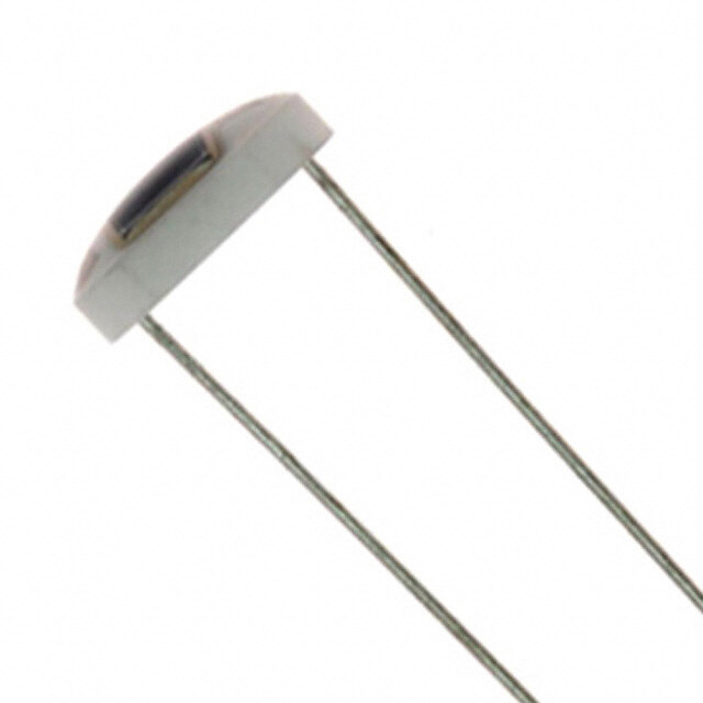
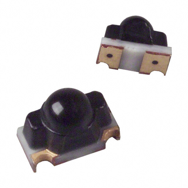
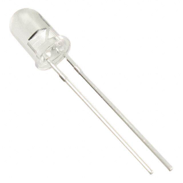
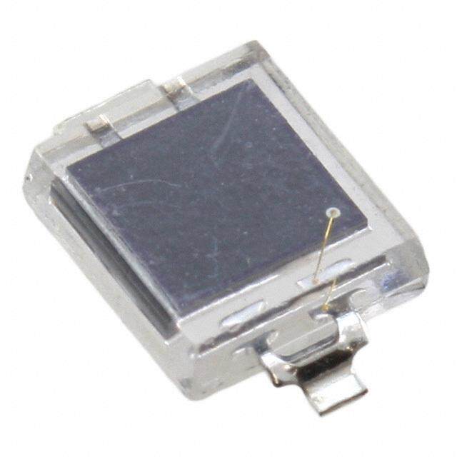
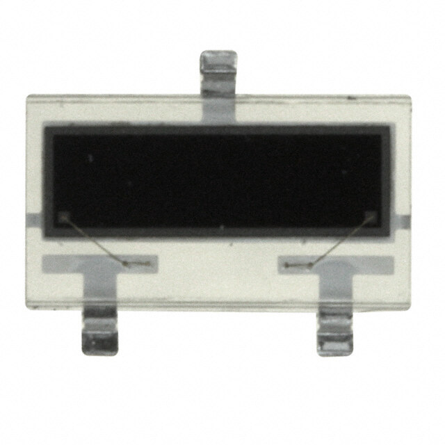
ICGOO电子元器件商城为您提供HSDL-5400#031由Lite-On设计生产,在icgoo商城现货销售,并且可以通过原厂、代理商等渠道进行代购。 HSDL-5400#031价格参考。Lite-OnHSDL-5400#031封装/规格:光学传感器 - 光电二极管, Photodiode 875nm 110° 2-SMD, Z-Bend。您可以下载HSDL-5400#031参考资料、Datasheet数据手册功能说明书,资料中有HSDL-5400#031 详细功能的应用电路图电压和使用方法及教程。
HSDL-5400#031 是隶属于 Lite-On Inc. 旗下的一款光电二极管传感器,属于光学传感器的一种。它通常用于检测可见光或近红外光,并将光信号转换为电信号,适用于多种自动化和检测系统。

该型号的典型应用场景包括:

1. 光控开关:用于自动照明系统,如路灯或室内照明,根据环境光强度自动开启或关闭灯具,实现节能。

2. 光学编码器:在工业自动化设备中,用于检测旋转或线性运动的位置、速度和方向,常见于电机控制和机器人系统中。

3. 安全系统:如红外线探测器或光幕系统,用于检测物体或人员的通过,广泛应用于门禁系统、自动门和安防设备。

4. 消费电子产品:例如用于手机、平板电脑等设备的环境光传感器,自动调节屏幕亮度以提升用户体验并延长电池寿命。

5. 测量仪器:用于光强测量、颜色识别或光谱分析设备中,作为光信号采集的核心元件。

6. 工业检测设备:用于生产线上的产品计数、位置检测或缺陷检测,提升生产效率和自动化水平。

HSDL-5400#031具备响应速度快、灵敏度高、稳定性好等特点,适合在多种光感应应用中使用。
| 参数 | 数值 |
| 产品目录 | |
| 描述 | PHOTODIODE PIN FLAT 110DEG ZBEND |
| 产品分类 | |
| 品牌 | Lite-On Inc |
| 数据手册 | |
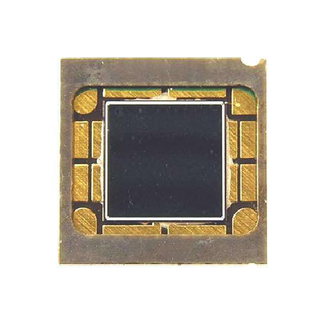
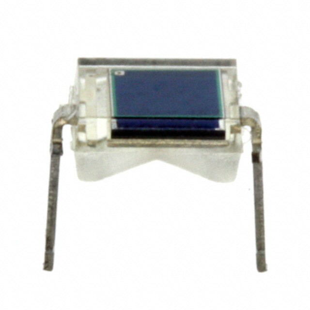
| 产品图片 |
|
| 产品型号 | HSDL-5400#031 |
| rohs | 无铅 / 符合限制有害物质指令(RoHS)规范要求 |
| 产品系列 | HSDL-5400 |
| 不同nm时的响应度 | - |
| 二极管类型 | 引脚 |
| 其它名称 | 160-1917-1 |
| 响应时间 | - |
| 封装/外壳 | 2-SMD,Z形弯曲d |
| 工作温度 | -40°C ~ 85°C |
| 有效面积 | 0.15mm² |
| 标准包装 | 1 |
| 波长 | 875nm |
| 电压-DC反向(Vr)(最大值) | 40V |
| 电流-暗(典型值) | 1nA |
| 视角 | 110° |
| 频谱范围 | 770nm ~ 1000nm |
| 颜色-增强 | - |


- 商务部:美国ITC正式对集成电路等产品启动337调查
- 曝三星4nm工艺存在良率问题 高通将骁龙8 Gen1或转产台积电
- 太阳诱电将投资9.5亿元在常州建新厂生产MLCC 预计2023年完工
- 英特尔发布欧洲新工厂建设计划 深化IDM 2.0 战略
- 台积电先进制程称霸业界 有大客户加持明年业绩稳了
- 达到5530亿美元!SIA预计今年全球半导体销售额将创下新高
- 英特尔拟将自动驾驶子公司Mobileye上市 估值或超500亿美元
- 三星加码芯片和SET,合并消费电子和移动部门,撤换高东真等 CEO
- 三星电子宣布重大人事变动 还合并消费电子和移动部门
- 海关总署:前11个月进口集成电路产品价值2.52万亿元 增长14.8%

PDF Datasheet 数据手册内容提取
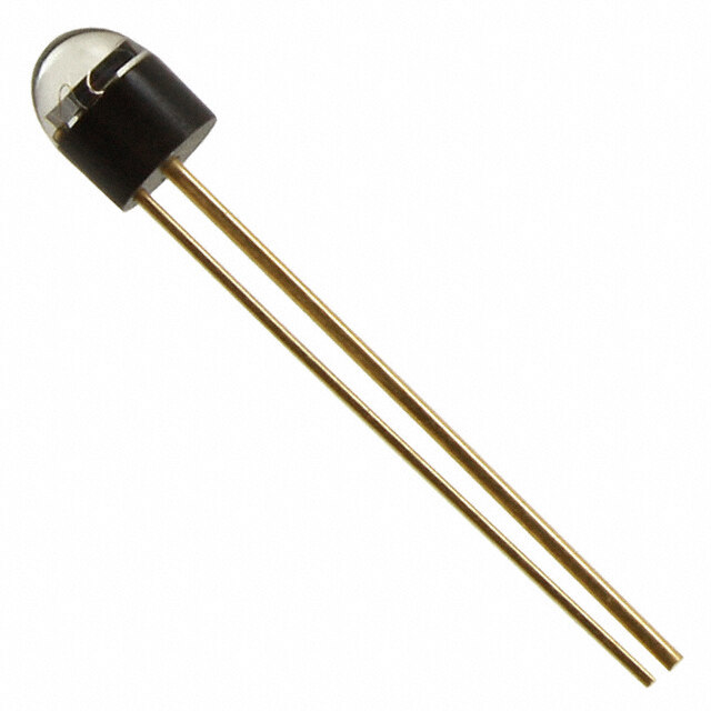
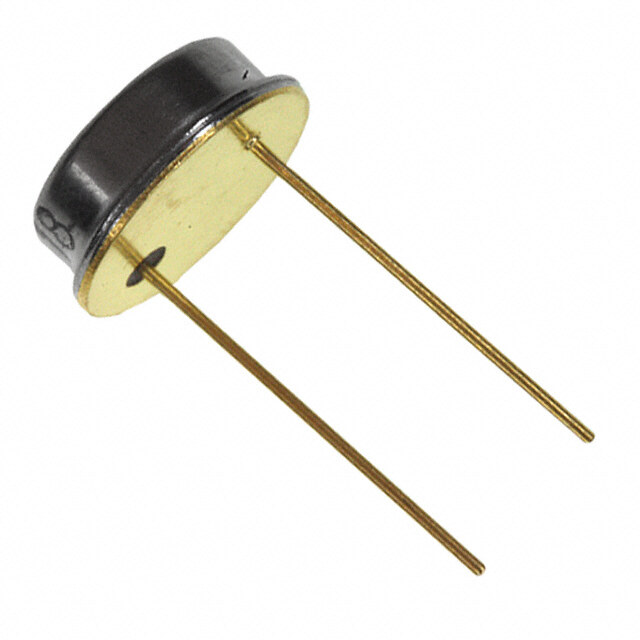
HSDL-44xx IR Emitter Series HSDL-54xx IR Detector Series High-Performance IR Emitter and IR PIN Photodiode in Subminiature SMT Package Data Sheet Description Features Flat Top Package • Subminiature flat top and dome package The HSDL-4400 Series of flat top IR emitters uses an Size – 2x2 mm untinted, nondiffused, truncated lens to provide a • IR emitter wide radiation pattern that is useful for short distance 875 nm TS AlGaAs communication where alignment of the emitter and Intensity – 17 mW/sr detector is not critical. The HSDL-5400 Series of flat Speed – 40 ns top IR detectors uses the same truncated lens design • Wide range of drive currents as the HSDL-4400 Series of IR emitters with the 500 µA to 500 mA added feature of a black tint that acts as an optical • IR detector filter to reduce the effects of ambient light, such as PIN photodiode sun, incandescent and fluorescent light from High sensitivity interfering with the IR signal. Speed – 7.5 ns • Flexible lead configurations Dome Package Surface mount or through hole The HSDL-4420 Series of dome IR emitters uses an untinted, nondiffused lens to provide a 24 degree Applications viewing angle with high on-axis intensity. The HSDL-5420 Series of IR detectors uses the same lens • Short distance IR links design as the HSDL-4420 IR emitter and optical filter • IrDA compatible used in the HSDL-5400 IR detector. • Small handheld devices Pagers Lead Configuration Industrial handhelds All of these devices are made by encapsulating LED • Diffuse LANs and PIN photodiode chips on axial lead frames to • Wireless audio form molded epoxy subminiature packages. A variety of lead configurations is available and includes: surface mount gull wing, yoke lead, or Z-bend and through hole lead bends at 2.54 mm (0.100 inch) center spacing. Technology The subminiature solid state emitters utilize a highly optimized LED material, transparent substrate aluminum gallium arsenide, TS AlGaAs. This material has a very high radiant efficiency, capable of pro- ducing high light output over a wide range of drive currents and temperature.
Device Selection Guide IR Emitters Part Number Device Description[1] Device Outline Drawing HSDL-4400 LED, Flat Top, 110 deg A HSDL-4420 LED, Dome, 24 deg B IR Detectors Part Number Device Description[1] Device Outline Drawing HSDL-5400 PIN Photodiode, Flat Top, 110 deg C HSDL-5420 PIN Photodiode, Dome, 28 deg D Package Configuration Options Option Package Code Package Configuration Description Outline Drawing 011 Gull Wing Lead, Tape and Reel[2] E, J, M 021 Yoke Lead, Tape and Reel[2] Surface Mount Lead F, K, M 031 Z-Bend, Tape and Reel[2] G, L, M 1L1 2.54 mm (0.100 in) Center Long Leads; 10.4 mm (0.410 in) Thru Hole Lead H 1S1 Lead Spacing Short Leads; 3.7 mm (0.145 in) I No Option Straight Leads[3] Prototyping A, B, C, D Notes: 1. IR Emitters have untinted, nondiffused lenses and IR Detectors have black tinted, nondiffused lenses. 2. Emitters and detectors are supplied in 12 mm embossed tape on 178 mm (7 inch) diameter reels, with 1500 units per reel. Minimum order quantity and order increment are in quantity of reels only. 3. Emitters and detectors are supplied in bulk form in bags of 50 units. 4. The HSDL-44xx and HSDL-54xx families are not designed to be used in medical devices with life support functions or in safety equipment (or similar applications where components failures would result in loss of life or physical harm), eg. in automotive, medical or airline industries. 2
Package Dimensions (A) Flat Top Emitters 1.40(0.055) 1.65(0.065) 0.50 (0.020) REF. NOTE 3 ANODE 1.14 (0.045) 1.40 (0.055) 0.58(0.023) 11.68(0.460) 0.43(0.017) 10.67(0.420) BOTH SIDES 1.91(0.075) 2.41(0.095) 0.76 (0.030) MAX. 0.46(0.018) CATHODE 0.56(0.022) CATHODE STRIPE 1.65(0.065)DIA. 2.08(0.082) NOTE 4 0.18(0.007) 1.91(0.075) 1.91(0.075) 0.25 (0.010) MAX.* 2.34(0.092) 0.23(0.009) 2.16(0.085) 0.20 (0.008) MAX. NOTE 2 (B) Dome Emitters 0.76(0.030) 0.18(0.007) R. 0.89(0.035) 0.23(0.009) 0.94(0.037) 1.24(0.049) 2.03 (0.080) 1.78 (0.070) 2.92 (0.115) MAX. 0.63(0.025) 0.79 (0.031) CATHODE 0.38(0.015) 0.53 (0.021) STRIPE 2.08(0.082) NOTE 4 1.91(0.075) 2.34(0.092) 2.16(0.085) 0.50 (0.020) REF. NOTE 3 ANODE 11.68(0.460) 10.67(0.420) BOTH SIDES 0.46(0.018) CATHODE 0.56(0.022) 1.65(0.065) DIA. 1.91(0.075) 0.25 (0.010) MAX.* 0.20 (0.008) MAX. NOTE 2 NOTES: 1. ALL DIMENSIONS ARE IN MILLIMETRES (INCHES). 2. PROTRUDING SUPPORT TAB IS CONNECTED TO ANODE LEAD. 3. LEAD POLARITY FOR THESE TS AlGaAs SUBMINIATURE LAMPS IS OPPOSITE TO THE LEAD POLARITY OF SUBMINIATURE LAMPS USING OTHER LED TECHNOLOGIES. 4. CATHODE STRIPE MARKING IS DARK BLUE. 3
(C) Flat Top Detectors 1.40(0.055) 1.65(0.065) 0.50 (0.020) REF. CATHODE 1.14 (0.045) 1.40 (0.055) 0.58(0.023) 11.68(0.460) 0.43(0.017) 10.67(0.420) BOTH SIDES 1.91(0.075) 2.41(0.095) 0.76 (0.030) MAX. 0.46(0.018) ANODE 0.56(0.022) CATHODE STRIPE 1.65(0.065)DIA. 2.08(0.082) NOTE 3 0.18(0.007) 1.91(0.075) 1.91(0.075) 0.25 (0.010) MAX.* 2.34(0.092) 0.23(0.009) 2.16(0.085) 0.20 (0.008) MAX. NOTE 2 (D) Dome Detectors 0.76(0.030) 0.18(0.007) R. 0.89(0.035) 0.23(0.009) 0.94(0.037) 1.24(0.049) 2.03 (0.080) 1.78 (0.070) 2.92 (0.115) MAX. 0.63(0.025) 0.79 (0.031) CATHODE 0.38(0.015) 0.53 (0.021) STRIPE 2.08(0.082) NOTE 3 1.91(0.075) 2.34(0.092) 2.16(0.085) 0.50 (0.020) REF. CATHODE 11.68(0.460) 10.67(0.420) BOTH SIDES 0.46(0.018) ANODE 0.56(0.022) 1.65(0.065) DIA. 1.91(0.075) 0.25 (0.010) MAX.* 0.20 (0.008) MAX. NOTE 2 NOTES: 1. ALL DIMENSIONS ARE IN MILLIMETRES (INCHES). 2. PROTRUDING SUPPORT TAB IS CONNECTED TO CATHODE LEAD. 3. CATHODE STRIPE MARKING IS DARK BLUE. 4
Package Dimensions reversed for the HSDL-44xx The following notes affect the IR emitters where the pro- package outline drawings E truding support tab is closest through I. to the cathode lead. 1. The pinout represents the 2. The protruding support tab of HSDL-54xx IR detectors the HSDL-54xx is connected where the protruding support to the cathode lead. While the tab is closest to the anode protruding support tab of the lead. While the pinout is HSDL-44xx is connected to the anode lead. (E) Gull Wing Lead, Option 011 0.76 (0.030) MAX. (F) “Yoke” Lead, Options 021 0.76 (0.030) MAX. ALL DIMENSIONS ARE IN MILLIMETRES (INCHES) 5
(G) Z-Bend Lead, Options 031 0.76 (0.030) MAX. (H) Thru Hole Lead Option 1L1 (I) Thru Hole Lead Option 1S1 6
Package Dimensions: Surface Mount Tape and Reel Options (J) 12 mm Tape and Reel, Gull Wing Lead, Option 011 NOTES: 1. EMPTY COMPONENT POCKETS SEALED WITH TOP COVER TAPE. 2. 7 INCH REEL – 1500 PIECES PER REEL. GULL WING LEAD 3. MINIMUM LEADER LENGTH AT EITHER END OF THE TAPE IS 500 mm. SUBMINIATURE PACKAGE 4. THE MAXIMUM NUMBER OF CONSECUTIVE MISSING DEVICES IS TWO. 5. IN ACCORDANCE WITH ANSI/EIA RS-481 SPECIFICATIONS, THE CATHODE IS ORIENTED TOWARDS THE TAPE SPROCKETS HOLE. 7
(K) 12 mm Tape and Reel, “Yoke” Lead, Option 021 “YOKE” LEAD SUBMINIATURE PACKAGE 8
(L) 12 mm Tape and Reel, Z-Bend Lead, Option 031 Z-BEND LEAD SUBMINIATURE PACKAGE 9
(M) 12 mm Tape and Reel Convective IR Reflow Soldering For information on IR reflow soldering, refer to Application Note 1060, Surface Mounting SMT LED Components. 10
HSDL-44xx Absolute Maximum Ratings Parameter Symbol Min. Max. Unit Ref. Peak Forward Current (Duty Factor = 20%, I 500 mA Fig. 7, 8 FPK Pulse Width = 100 µs) DC Forward Current I 100 mA Fig. 6 FDC Power Dissipation P 100 mW DISS Reverse Voltage (I = 100 µA) V 5 V R R Transient Forward Current (10 µs Pulse) I 1.0 A [1] FTR Operating Temperature T -40 85 °C O Storage Temperature T -55 100 °C S Junction Temperature T 110 °C J Lead Solder Temperature 260/5 s °C [1.6 mm (0.063 in.) from body] Reflow Soldering Temperatures Convection IR 235/90 s °C Fig. 20 Vapor Phase 215/180 s °C Note: 1. The transient peak current in the maximum nonrecurring peak current the device can withstand without damaging the LED die and the wire bonds. HSDL-44xx Electrical Characteristics at T = 25°C A Parameter Symbol Min. Typ. Max. Unit Condition Ref. Forward Voltage V 1.30 1.50 1.70 V I = 50 mA Fig. 2 F FDC 2.15 I = 250 mA FPK Forward Voltage ∆V /∆T -2.1 mV/°C I = 50 mA Fig. 3 F FDC Temperature Coefficient -2.1 I = 100 mA FDC Series Resistance R 2 Ω I = 100 mA S FDC Diode Capacitance C 50 pF 0 V, 1 MHz O Reverse Voltage V 5 20 V I = 100 µA R R Thermal Resistance, Rq 170 °C/W jp Junction to Pin 11
HSDL-44XX Optical Characteristics at T = 25°C A Parameter Symbol Min. Typ. Max. Unit Condition Ref. Radiant On-Axis Intensity HSDL-4400 I 1 3 8 mW/sr I = 50 mA Fig. 4, 5 E FDC 6 I = 100 mA FDC 15 I = 250 mA FPK HSDL-4420 I 9 17 30 mW/sr I = 50 mA Fig. 4, 5 E FDC 32 I = 100 mA FDC 85 I = 250 mA FPK Radiant On-Axis Intensity ∆I /∆T -0.35 %/°C I = 50 mA E FDC Temperature Coefficient -0.35 I = 100 mA FDC Viewing Angle HSDL-4400 2q 110 deg I = 50 mA Fig. 9 1/2 FDC HSDL-4420 2q 24 deg I = 50 mA Fig. 10 1/2 FDC Peak Wavelength l 850 875 900 nm I = 50 mA Fig. 1 PK FDC Peak Wavelength ∆l/∆T 0.25 nm/°C I = 50 mA FDC Temperature Coefficient Spectral Width at FWHM ∆l 37 nm I = 50 mA Fig. 1 FDC Optical Rise and Fall t/t 40 ns I = 50 mA r f FPK Times, 10%-90% Bandwidth f 9 MHz I = 50 mA Fig. 11 c FDC ± 10 mA 12
HSDL-54xx Absolute Maximum Ratings Parameter Symbol Min. Max. Unit Power Dissipation P 150 mW DISS Reverse Voltage (I = 100 µA) V 40 V R R Operating Temperature T -40 85 °C O Storage Temperature T -55 100 °C S Junction Temperature T 110 °C J Lead Solder Temperature [1.6 mm (0.063 in.) from body] 260/5 s °C Reflow Soldering Temperatures Convection IR 235/90 s °C Vapor Phase 215/180 s °C HSDL-54xx Electrical Characteristics at T = 25°C A Parameter Symbol Min. Typ. Max. Unit Condition Ref. Forward Voltage V 0.8 V I = 1 mA F FDC Breakdown Voltage V 40 V I = 100 µA, BR R E = 0 mW/cm2 e Reverse Dark Current I 1 5 nA V = 5 V, Fig. 12 D R E = 0 mW/cm2 e Series Resistance R 2000 Ω V = 5 V, S R E = 0 mW/cm2 e Diode Capacitance C 5 pF V = 0 V, Fig. 16 O R E = 0 mW/cm2 e f = 1 MHz Open Circuit Voltage V 375 mV E = 1 mW/cm2 OC e l = 875 nm PK Temperature Coefficient of V ∆V /∆T -2.2 mV/K E = 1 mW/cm2 OC OC e l = 875 nm PK Short Circuit Current I E = 1 mW/cm2 SC e HSDL-5400 1.6 µA lPK = 875 nm HSDL-5420 4.3 µA Temperature Coefficient of I ∆I /∆T 0.16 %/K E = 1 mW/cm2 SC SC e l = 875 nm PK Thermal Resistance, Rq 170 °C/W jp Junction to Pin 13
HSDL-54xx Optical Characteristics at T = 25°C A Parameter Symbol Min. Typ. Max. Unit Condition Ref. Photocurrent E = 1 mW/cm2 Fig 14, e HSDL-5400 I 0.8 1.6 µA l = 875 nm 15 PH PK HSDL-5420 3.0 6.0 V = 5 V R Temperature Coefficient of I ∆I /∆T 0.1 %/K E = 1 mW/cm2 Fig. 13 PH PH e l = 875 nm PK V = 5 V R Radiant Sensitive Area A 0.15 mm2 Absolute Spectral Sensitivity S 0.5 A/W E = 1 mW/cm2 e l = 875 nm PK V = 5 V R Viewing Angle HSDL-5400 2q 110 deg Fig. 18 1/2 HSDL-5420 28 Fig. 19 Wavelength of Peak Sensitivity l 875 nm E = 1 mW/cm2 Fig. 17 PK e V = 5 V R Spectral Bandwidth ∆l 770- nm E = 1 mW/cm2 Fig. 17 e 1000 V = 5 V R Quantum Efficiency h 70 % E = 1 mW/cm2 e l = 875 nm, PK V = 5 V R Noise Equivalent Power NEP 6.2 x W/Hz1/2 V = 5 V R 10-15 l = 875 nm PK Detectivity D 6.3 x cm* V = 5 V R 1012 Hz1/2/W l = 875 nm PK Optical Rise and Fall Times, 10%-90% t/t 7.5 ns V = 5 V r f R R = 1 kΩ L l = 875 nm PK Bandwidth f 50 MHz V = 5 V c R R = 1 kΩ L l = 875 nm PK 14
1.5 Am 1,000 2.0 NTENSITY 1.0 TIFAD C= 2=5 5 °0C mA – TNERRUC 100 TA = 25 °C TAGE – V 1.8 IFDC = 100 mA NT I DR VOL 1.6 IFDC = 50 mA DIA AW RD A R A 1.4 R O W RELATIVE 0.5 F KAEP – K 10 V – FORF 1.2 IFDC = 1 mA 0800 850 900 950 IPF 10 0.5 1.0 1.5 2.0 2.5 3.0 1.0-20 0 20 40 60 80 λ – WAVELENGTH – nm VF – FORWARD VOLTAGE – V TA – AMBIENT TEMPERATURE – °C Figure 1. Relative radiant intensity vs. Figure 2. Peak forward current vs. forward Figure 3. Forward voltage vs. ambient wavelength. voltage. temperature. A m 5.00 1.00 – 120 T Y Y N SIT 4.50 PULSE WIDTHS < 100 µs SIT RE 100 TEN 4.00 TA = 25°C TEN TA = 25°C CUR Rθja = 220 °C/W T IN 3.50 T IN RD 80 Rθja = 270 °C/W AN 3.00 AN WA Rθja = 370 °C/W DI 2.50 DI 0.10 R 60 A A O D R 2.00 D R C F E E D 40 ORMALIZ 011...505000 ORMALIZ AXIMUM 20 N 0 N 0.01 – M 0 0 100 200 300 400 500 0.1 1 10 C -40 -20 0 20 40 60 80 100 D IFPK – PEAK FORWARD CURRENT – mA IFPK – FORWARD CURRENT – mA IF TA – AMBIENT TEMPERATURE – °C Figure 4. Normalized radiant intensity vs. Figure 5. Normalized radiant intensity vs. Figure 6. Maximum DC forward current vs. peak forward current. peak forward current (0 to 10 mA). ambient temperature. Derated based on T = 110°C. JMAX A 500 A 600 URRENT – m 400 DUTY FA7125C 000% T%%%OR URRENT – m 540000 DUTY FA1C0 T%OR 10 % D C 300 D C 2500 %% 20 % AR AR 300 W W R 200 R O O 200 F F EAK 100 EAK 100 50 % P P – K – K PULSE WIDTHS < 100 µs P 0 P 0 IF 0.01 0.1 1 10 IF -40 -20 0 20 40 60 80 100 tPW – PULSE WIDTH – ms TA – AMBIENT TEMPERATURE – °C Figure 7. Maximum peak forward current vs. Figure 8. Maximum peak forward current vs. duty factor. ambient temperature. Derated based on T = 110°C. JMAX 15
1.0 IF = 50 mA Y 0.9 SIT 0.8 TA = 25°C N TE 0.7 N T I 0.6 N A 0.5 DI A 0.4 R E 0.3 V ATI 0.2 L RE 0.1 0 -100° -80° -60° -40° -20° 0° 20° 40° 60° 80° 100° θ – ANGLE FROM OPTICAL CENTERLINE – DEGREES (CONE HALF ANGLE) Figure 9. Relative radiant intensity vs. angular displacement HSDL-4400. 1.0 Y 0.9 SIT 0.8 IF = 50 mA TEN 0.7 TA = 25°C N T I 0.6 N A 0.5 DI A 0.4 R E 0.3 V ATI 0.2 L RE 0.1 0 -50° -40° -30° -20° -10° 0° 10° 20° 30° 40° 50° θ – ANGLE FROM OPTICAL CENTERLINE – DEGREES (CONE HALF ANGLE) Figure 10. Relative radiant intensity vs. angular displacement HSDL-4420. 2 10.000 1.40 A NT INTENSITY ---10123 T9 AM =H 2z5°C CURRENT – n 1.000 VR = 5 V TOCURRENT 111...231000 VR = 5 V RADIA --45 DARK 0.100 D PHO 1.00 RELATIVE ----7689 – REVERSE 0.010 NORMALIZE 000...897000 -10 I D 0.001 0.60 1E+5 1E+6 1E+7 1E+8 0 20 40 60 80 100 -40 -20 0 20 40 60 80 100 f – FREQUENCY – Hz TA – AMBIENT TEMPERATURE – °C TA – AMBIENT TEMPERATURE – °C Figure 11. Relative radiant intensity vs. Figure 12. Reverse dark current vs. ambient Figure 13. Relative reverse light current vs. frequency. temperature. ambient temperature. 16
10 1.40 NT VR = 5 V NT 1.30 RRE TA = 25°C RRE 1.20 TA = 25°C U U C 1 C O O 1.10 T T O O H H 1.00 P P D D E E 0.90 Z 0.1 Z LI LI A A 0.80 M M R R O O 0.70 N N 0.01 0.60 0.01 0.1 1 10 0 5 10 15 20 25 30 35 40 Ee – IRRADIANCE – mW/cm2 VR – REVERSE VOLTAGE – V Figure 14. Reverse light current vs. irradiance Figure 15. Reverse light current vs. reverse voltage. 5 1.2 CE – pF 4 EfT =eA =1= M02 5Hm°zCW/cm2 RRENT 1.0 TVAR = = 2 55 °VC AN CU 0.8 CAPACIT 32 D PHOTO 0.6 DIODE 1 MALIZE 0.4 – R 0.2 O O C N 0 0 0.1 1 10 100 700750 800 850 900 950100010501100 VR – REVERSE VOLTAGE – V λ – WAVELENGTH – nm Figure 16. Diode capacitance vs. reverse Figure 17. Relative spectral sensitivity vs. voltage. wavelength. At the time of this publication, Light Emitting Diodes (LEDs) that are contained in this product are regulated for eye safety in Europe by the Commission for European Electrotechnical Standardization (CENELEC) EN60825-1. Please refer to Application Brief I-008 for more information. 17
1.0 VR = 5 V T 0.9 REN 0.8 TA = 25°C R U 0.7 C O 0.6 T O H 0.5 P D 0.4 E Z LI 0.3 A M 0.2 R O 0.1 N 0 -100° -80° -60° -40° -20° 0° 20° 40° 60° 80° 100° θ – ANGLE FROM OPTICAL CENTERLINE – DEGREES (CONE HALF ANGLE) Figure 18. Relative radiant intensity vs. angular displacement. HSDL-5400. 1.0 T 0.9 N RE 0.8 R U 0.7 C O 0.6 T O H 0.5 P D 0.4 E Z LI 0.3 A M 0.2 R O 0.1 N 0 -50° -40° -30° -20° -10° 0° 10° 20° 30° 40° 50° θ – ANGLE FROM OPTICAL CENTERLINE – DEGREES (CONE HALF ANGLE) Figure 19. Relative radiant intensity vs. angular displacement. HSDL-5420. 18
MAX. 260°C 255 R3 R4 C) 230 – (° 220200 RE 180 R2 60 sec. U MAX. AT 160 ABOVE PER 120 R1 220°C R5 M E T 80 – T 25 0 50 100 150 200 250 300 t-TIME (SECONDS) P1 P2 P3 P4 HEAT SOLDER PASTE DRY SOLDER COOL UP REFLOW DOWN Process Zone Symbol DT Maximum DT/Dtime Heat Up P1, R1 25°C to 160°C 4°C/s Solder Paste Dry P2, R2 160°C to 200°C 0.5°C/s Solder Reflow P3, R3 200°C to 255°C (260°C at 10 seconds max) 4°C/s P3, R4 255°C to 200°C -6°C/s Cool Down P4, R5 200°C to 25°C -6°C/s Figure 20. Evaluation soldering profiles (polyled). For company and product information, please go to our web site: WWW.liteon.com or http://optodatabook.liteon.com/databook/databook.aspx Data subject to change. Copyright © 2007 Lite-On Technology Corporation. All rights reserved.