首页 > HMC985LP4KE > 详情
 Datasheet下载
- 型号: HMC985LP4KE
- 制造商: Hittite
- 库位|库存: xxxx|xxxx
- 要求:
| 数量阶梯 | 香港交货 | 国内含税 |
| +xxxx | $xxxx | ¥xxxx |
查看当月历史价格
查看今年历史价格
产品参数
| 参数 | 数值 |
| 产品目录 | 射频/IF 和 RFID |
| 描述 | IC ATTENUATOR VVA MMIC 24SMD |
| 产品分类 | 衰减器 |
| 品牌 | Hittite Microwave Corporation |
| 数据手册 | 点击此处下载产品Datasheet |
| 产品图片 |  |
| 产品型号 | HMC985LP4KE |
| rohs | 无铅 / 符合限制有害物质指令(RoHS)规范要求 |
| 产品系列 | - |
| 其它名称 | 1127-1827 |
| 功率(W) | - |
| 容差 | - |
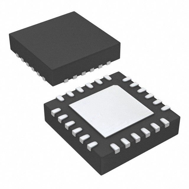
| 封装/外壳 | 24-VFQFN 裸露焊盘 |
| 标准包装 | 1 |
| 衰减值 | - |
| 阻抗 | 50 欧姆 |
| 频率范围 | 10GHz ~ 40GHz |
Datasheet
PDF Datasheet 数据手册内容提取
HMC985LP4KE v01.0813 GaAs MMIC VOLTAGE - VARIABLE ATTENUATOR, 10 - 40 GHz Typical Applications Features the HMC985lP4Ke is ideal for: Wide Bandwidth: 10 - 40 gHz t excellent linearity: +32 dB Input IP3 • Point-to-Point radio M Wide attenuation range: 35 dB • Vsat radio s no external Matching • test Instrumentation - 24 lead 4x4 mm sMt Package: 16 mm² g • Microwave sensors o • Military, eCM & radar General Description l a the HMC985lP4Ke is an absorptive Voltage Variable n Functional Diagram attenuator (VVa) which operates from 10 - 40 gHz and a is ideal in designs where an analog DC control signal - must be used to control rF signal levels over a 35 dB s dynamic range. It features two shunt-type attenuators which are controlled by two analog voltages, Vctl1 and r Vctl2. optimum linearity performance of the attenuator o is achieved by first varying Vctl1 of the first attenuation t stage from -3V to 0V with Vctl2 fixed at -3V. the control a voltage of the second attenuation stage, Vctl2, should u then be varied from -3V to 0V with Vctl1 fixed at 0V. n if the Vctl1 and Vctl2 pins are connected together it is e possible to achieve the full analog attenuation range t with only a small degradation in input IP3 performance. t applications include agC circuits and temperature a compensation of multiple gain stages in microwave point-to-point and Vsat radios. Electrical Specifications, T = +25 °C, Test Condition Vctl1 = Vctl2 A Parameter Frequency Min. typ. Max. units 10 - 20 gHz 3 3.5 dB Insertion loss [1] 20 - 30 gHz 3 4 dB 30 -40 gHz 3.5 4.5 dB 10 - 20 gHz 25 30 dB attenuation range 20 - 30 gHz 30 35 dB 30 - 40 gHz 35 40 dB Input return loss 10 - 40 gHz 13 dB output return loss 10 - 40 gHz 13 dB Input third order Intercept 33 dBm (two-tone input Power = 10 dBm each tone) [2] [1] Vcntl1 = Vcntl2 =-2.4V [2] Vcntl1 = Vcntl2 =-2.0V worst case InfoFrmoart iopn rfiucrneis,h edde blyi vAenraylo ga Dnedvic teos ips lbaelcieeve do rtod beer sac:c Huraittet iatned Mreliiacbrleo. wHoawveeve rC, noo rpoForar tpioricne,, 2d eElilviezrayb, aentdh tDo rpivlaec,e C ohrdeelrms: sAfonardlo,g MDeAv i0ce1s8, 2In4c., responsibility is assumed by Analog Devices for its use, nor for any infringements of patents or other One Technology Way, P.O. Box 9106, Norwood, MA 02062-9106 1 rliicgehntss eo fi sth girrda nptaerdti ebsy t himatp mlicaaPyt iorhenso uonlrt ofertoh:m e9r wit7sis 8ues -eu2.n dS5ep0re ca-inf3iyc 3aptia4otne3sn ts ou rb jpeFacttae tnoxt c:r hig9ahn7tgs 8eo wf- 2Aithn5oau0lot g-n 3oDti3ecve7i.c 3eNso . POhrodnee:r 7 O81n-3-2li9n-e4 7a0t0 w(cid:127) wOrwde.hr oitntliitnee. cato wmww.analog.com Trademarks and registered trademarks arAe tphep plriocpearttyi oof nth eSir urespppecotivret :o wPnehrso.ne: 978-250-3A3p4p3li c aotrio na Spuppsp@orht: iPtthitoen.ec: o1-m800-ANALOG-D
HMC985LP4KE v01.0813 GaAs MMIC VOLTAGE - VARIABLE ATTENUATOR, 10 - 40 GHz Attenuation vs. Frequency over Vctl1 = Attenuation vs. Frequency over Vctl1 = Variable, Vctl2 = -3V 0V, Vctl2 = Variable 0 0 -10 t -5 ON (dB)-10 ON (dB)--3200 sM ATTENUATI-15 ATTENUATI--5400 g - -20 o -60 l -25 -70 a 10 15 20 25 30 35 40 10 15 20 25 30 35 40 n FREQUENCY (GHz) FREQUENCY (GHz) a ---221...406VVV - 1--00.2..84VVV 0.0V ---221...406VVV - 1--00.2..84VVV 0.0V - s Attenuation vs. Vctl1 Attenuation vs. Vctl2 r Over Temperature @ 25 GHz, Vctl2 = -3V Over Temperature @ 30 GHz, Vctl1 = 0V o 0 0 t -5 a -3 -10 u dB) dB)-15 n N ( -6 N ( O O-20 e TI TI UA UA-25 t N -9 N TE TE-30 t T T A A a -12 -35 -40 -15 -45 -2.4 -2 -1.6 -1.2 -0.8 -0.4 0 -2.4 -2 -1.6 -1.2 -0.8 -0.4 0 Vctrl1 (V) Vctrl1 (V) +25 C +85 C -40 C +25 C +85 C -40 C Attenuation vs. Pin @ 20 GHz over Vctl1 Attenuation vs. Pin @ 20 GHz over Vctl2 Vctl1 = Variable, Vctl2 = -3V Vctl2 = Variable, Vctl1 = 0V 0 0 -4 -10 dB) -8 dB) N ( N (-20 O O TI-12 TI A A U U N N-30 TE-16 TE T T A A -40 -20 -24 -50 -5 -1 3 7 11 15 -5 -1 3 7 11 15 INPUT POWER (dBm) INPUT POWER (dBm) -2.4V -1.2V 0.0V -2.4V -1.2V 0.0V -2.0V -0.8V -2.0V -0.8V -1.6V -0.4V -1.6V -0.4V InfoFrmoart iopn rfiucrneis,h edde blyi vAenraylo ga Dnedvic teos ips lbaelcieeve do rtod beer sac:c Huraittet iatned Mreliiacbrleo. wHoawveeve rC, noo rpoForar tpioricne,, 2d eElilviezrayb, aentdh tDo rpivlaec,e C ohrdeelrms: sAfonardlo,g MDeAv i0ce1s8, 2In4c., responsibility is assumed by Analog Devices for its use, nor for any infringements of patents or other One Technology Way, P.O. Box 9106, Norwood, MA 02062-9106 rights of third parties that maPy rhesounlt fero:m 9 it7s 8us-e2. S5p0ec-if3ic3ati4on3s s u b jeFcta tox c: h9an7g8e w-2ith5ou0t -n3oti3ce7. 3No POhrodnee:r 7 O81n-3-2li9n-e4 7a0t0 w(cid:127) wOrwde.hr oitntliitnee. cato wmww.analog.com 2 license is granted by implication or otherwise under any patent or patent rights of Analog Devices. Trademarks and registered trademarks arAe tphep plriocpearttyi oof nth eSir urespppecotivret :o wPnehrso.ne: 978-250-3A3p4p3li c aotrio na Spuppsp@orht: iPtthitoen.ec: o1-m800-ANALOG-D
HMC985LP4KE v01.0813 GaAs MMIC VOLTAGE - VARIABLE ATTENUATOR, 10 - 40 GHz Input Return Loss Input Return Loss Vctl1 = Variable, Vctl2 = -3V Vctl1 = 0V, Vctl2 = Variable 0 0 t sM S (dB)-10 S (dB)-10 - N LOS-20 N LOS-20 g RETUR-30 RETUR-30 o l a -40 -40 10 15 20 25 30 35 40 10 15 20 25 30 35 40 n FREQUENCY (GHz) FREQUENCY (GHz) a -2.4 V -1.2V 0.0 V -2.4 V -1.2V 0.0 V - s Output Return Loss Output Return Loss r Vctl1 = Variable, Vctl2 = -3V Vctl1 = 0V, Vctl2 = Variable o t 0 0 a u -10 -10 n dB) dB) S ( S ( e S S LO-20 LO-20 t N N R R t TU TU E E a R-30 R-30 -40 -40 10 15 20 25 30 35 40 10 15 20 25 30 35 40 FREQUENCY (GHz) FREQUENCY (GHz) -2.4 V -1.2V 0.0 V -2.4 V -1.2V 0.0 V Input IP3 vs. Input Power @ 20 GHz Input IP3 vs. Input Power Over Frequency Vctl1 = Variable, Vctl2 = -3V Vctl1 = -2V, Vctl2 = -3V [1] 60 45 50 41 m) 40 m) 37 B B d d P3 ( 30 P3 ( 33 I I 20 29 10 25 -5 -1 3 7 11 15 -5 -3 -1 1 3 5 7 9 11 13 15 SINGLE TONE INPUT POWER (dBm) SINGLE TONE INPUT POWER (dBm) -2.4V -1.2V 0.0V 10 GHz 20 GHz 30 GHz -2.0V -0.8V -1.6V -0.4V [1] Worst Case IP3 InfoFrmoart iopn rfiucrneis,h edde blyi vAenraylo ga Dnedvic teos ips lbaelcieeve do rtod beer sac:c Huraittet iatned Mreliiacbrleo. wHoawveeve rC, noo rpoForar tpioricne,, 2d eElilviezrayb, aentdh tDo rpivlaec,e C ohrdeelrms: sAfonardlo,g MDeAv i0ce1s8, 2In4c., responsibility is assumed by Analog Devices for its use, nor for any infringements of patents or other One Technology Way, P.O. Box 9106, Norwood, MA 02062-9106 3 rliicgehntss eo fi sth girrda nptaerdti ebsy t himatp mlicaaPyt iorhenso uonlrt ofertoh:m e9r wit7sis 8ues -eu2.n dS5ep0re ca-inf3iyc 3aptia4otne3sn ts ou rb jpeFacttae tnoxt c:r hig9ahn7tgs 8eo wf- 2Aithn5oau0lot g-n 3oDti3ecve7i.c 3eNso . POhrodnee:r 7 O81n-3-2li9n-e4 7a0t0 w(cid:127) wOrwde.hr oitntliitnee. cato wmww.analog.com Trademarks and registered trademarks arAe tphep plriocpearttyi oof nth eSir urespppecotivret :o wPnehrso.ne: 978-250-3A3p4p3li c aotrio na Spuppsp@orht: iPtthitoen.ec: o1-m800-ANALOG-D
HMC985LP4KE v01.0813 GaAs MMIC VOLTAGE - VARIABLE ATTENUATOR, 10 - 40 GHz Input IP3 vs. Input Power Over Temperature Input IP3 vs. Input Power @ 20 GHz @ 20 GHz, Vctl1 = -2V, Vctl2 = -3V [1] Vctl2 = Variable, Vctl1 = 0V 45 60 t 41 50 M m) 37 m) 40 s B B d d IP3 ( 33 IP3 ( 30 g - 29 20 o l 25 10 a -5 -3 -1 1 3 5 7 9 11 13 15 0 3 6 9 12 15 n SINGLE TONE INPUT POWER (dBm) SINGLE TONE INPUT POWER (dBm) a +25 C +85 C -40 C -2.4V -1.2V 0.0 V -2.0V -0.8V -1.6V -0.4V - s Input IP3 vs. Input Power Over Frequency Input IP3 vs Input Power over Tempera- r Vctl2 = -2V, Vctl1 = 0V [1] ture @ 20 GHz, Vctl2 = -2V, Vctl1 = 0V [1] o 45 45 t a 41 41 u n m) 37 m) 37 e B B d d P3 ( 33 P3 ( 33 t I I t a 29 29 25 25 0 3 6 9 12 15 0 3 6 9 12 15 SINGLE TONE INPUT POWER (dBm) SINGLE TONE INPUT POWER (dBm) 10 GHz 20 GHz 30 GHz +25 C +85 C -40 C [1] Worst Case IP3 InfoFrmoart iopn rfiucrneis,h edde blyi vAenraylo ga Dnedvic teos ips lbaelcieeve do rtod beer sac:c Huraittet iatned Mreliiacbrleo. wHoawveeve rC, noo rpoForar tpioricne,, 2d eElilviezrayb, aentdh tDo rpivlaec,e C ohrdeelrms: sAfonardlo,g MDeAv i0ce1s8, 2In4c., responsibility is assumed by Analog Devices for its use, nor for any infringements of patents or other One Technology Way, P.O. Box 9106, Norwood, MA 02062-9106 rights of third parties that maPy rhesounlt fero:m 9 it7s 8us-e2. S5p0ec-if3ic3ati4on3s s u b jeFcta tox c: h9an7g8e w-2ith5ou0t -n3oti3ce7. 3No POhrodnee:r 7 O81n-3-2li9n-e4 7a0t0 w(cid:127) wOrwde.hr oitntliitnee. cato wmww.analog.com 4 license is granted by implication or otherwise under any patent or patent rights of Analog Devices. Trademarks and registered trademarks arAe tphep plriocpearttyi oof nth eSir urespppecotivret :o wPnehrso.ne: 978-250-3A3p4p3li c aotrio na Spuppsp@orht: iPtthitoen.ec: o1-m800-ANALOG-D
HMC985LP4KE v01.0813 GaAs MMIC VOLTAGE - VARIABLE ATTENUATOR, 10 - 40 GHz Attenuation vs Frequency Over Vctrl Attenuation vs. Vctrl Over Temperature Vctl1 = Vctl2 @ 20 GHz, Vctl1 = Vctl2 0 0 -5 t -10 -10 sM N (dB)-20 N (dB)-15 O O-20 - UATI-30 UATI-25 g TEN-40 TEN-30 T T A A o -35 -50 -40 l a -60 -45 5 10 15 20 25 30 35 40 -2.4 -2 -1.6 -1.2 -0.8 -0.4 0 n FREQUENCY (GHz) Vctrl1 (V) a -2.4 V -1.2 V 0.0 V +25 C +85 C -40 C - --21..06 VV --00..84 VV s r Attenuation vs. Pin @ 20 GHz Over Vctl o Vctl1 = Vctl2 Input Return Loss, Vctl1 = Vctl2 t 0 0 a u -10 -10 n N (dB)-20 S (dB) e O S t UATI N LO-20 N-30 R t TTE ETU a A R-30 -40 -50 -40 -5 -1 3 7 11 15 10 15 20 25 30 35 40 INPUT POWER (dBm) FREQUENCY (GHz) -2.4V -1.2V 0.0V -2.4 V -1.2V 0.0 V -2.0V -0.8V -1.6V -0.4V Input IP3 vs. Input Power Over Vctrl @ 20 GHz, Vctl1 = Vctl2 Output Return Loss, Vctl1 = Vctl2 0 60 50 -10 B) d SS ( m) 40 URN LO-20 IP3 (dB 30 T E R-30 20 -40 10 10 15 20 25 30 35 40 0 3 6 9 12 15 FREQUENCY (GHz) SINGLE TONE INPUT POWER (dBm) -2.4 V -1.2V 0.0 V -2.4V -1.2V 0.0V -2.0V -0.8V -1.6V -0.4V InfoFrmoart iopn rfiucrneis,h edde blyi vAenraylo ga Dnedvic teos ips lbaelcieeve do rtod beer sac:c Huraittet iatned Mreliiacbrleo. wHoawveeve rC, noo rpoForar tpioricne,, 2d eElilviezrayb, aentdh tDo rpivlaec,e C ohrdeelrms: sAfonardlo,g MDeAv i0ce1s8, 2In4c., responsibility is assumed by Analog Devices for its use, nor for any infringements of patents or other One Technology Way, P.O. Box 9106, Norwood, MA 02062-9106 5 rliicgehntss eo fi sth girrda nptaerdti ebsy t himatp mlicaaPyt iorhenso uonlrt ofertoh:m e9r wit7sis 8ues -eu2.n dS5ep0re ca-inf3iyc 3aptia4otne3sn ts ou rb jpeFacttae tnoxt c:r hig9ahn7tgs 8eo wf- 2Aithn5oau0lot g-n 3oDti3ecve7i.c 3eNso . POhrodnee:r 7 O81n-3-2li9n-e4 7a0t0 w(cid:127) wOrwde.hr oitntliitnee. cato wmww.analog.com Trademarks and registered trademarks arAe tphep plriocpearttyi oof nth eSir urespppecotivret :o wPnehrso.ne: 978-250-3A3p4p3li c aotrio na Spuppsp@orht: iPtthitoen.ec: o1-m800-ANALOG-D
HMC985LP4KE v01.0813 GaAs MMIC VOLTAGE - VARIABLE ATTENUATOR, 10 - 40 GHz Input IP3 vs. Input Power Over Frequency Input IP3 vs. Input Power Over Vctl1 = Vctl2 Temperature @ 20 GHz Vctl1 = Vctl2 40 40 t 36 36 M m) 32 m) 32 s B B d d IP3 ( 28 IP3 ( 28 g - 24 24 o l 20 20 a -5 -1 3 7 11 15 -5 -1 3 7 11 15 n SINGLE TONE INPUT POWER (dBm) SINGLE TONE INPUT POWER (dBm) a 10 GHz 20 GHz 30 GHz +25 C +85 C -40 C - s r o t a u n e t t a InfoFrmoart iopn rfiucrneis,h edde blyi vAenraylo ga Dnedvic teos ips lbaelcieeve do rtod beer sac:c Huraittet iatned Mreliiacbrleo. wHoawveeve rC, noo rpoForar tpioricne,, 2d eElilviezrayb, aentdh tDo rpivlaec,e C ohrdeelrms: sAfonardlo,g MDeAv i0ce1s8, 2In4c., responsibility is assumed by Analog Devices for its use, nor for any infringements of patents or other One Technology Way, P.O. Box 9106, Norwood, MA 02062-9106 rights of third parties that maPy rhesounlt fero:m 9 it7s 8us-e2. S5p0ec-if3ic3ati4on3s s u b jeFcta tox c: h9an7g8e w-2ith5ou0t -n3oti3ce7. 3No POhrodnee:r 7 O81n-3-2li9n-e4 7a0t0 w(cid:127) wOrwde.hr oitntliitnee. cato wmww.analog.com 6 license is granted by implication or otherwise under any patent or patent rights of Analog Devices. Trademarks and registered trademarks arAe tphep plriocpearttyi oof nth eSir urespppecotivret :o wPnehrso.ne: 978-250-3A3p4p3li c aotrio na Spuppsp@orht: iPtthitoen.ec: o1-m800-ANALOG-D
HMC985LP4KE v01.0813 GaAs MMIC VOLTAGE - VARIABLE ATTENUATOR, 10 - 40 GHz Absolute Maximum Ratings Control Voltage +1 to -5V t Input rF Power 30 dBm eleCtrostatIC sensItIVe DeVICe M Maximum Junction temperature 165 °C oBserVe HanDlIng PreCautIons s thermal resistance (rtH) 62 °C/W (junction to ground paddle) - operating temperature -40°C to +85°C g storage temperature -65°C to 125°C o esD sensitivity (HBM) Class1a, passed 250V l a n a Outline Drawing - s r o t a u n e t t a notes: 1. PaCKage BoDY MaterIal: loW stress InJeCtIon MolDeD PlastIC sIlICa anD sIlICon IMPregnateD. 2. leaD anD grounD PaDDle MaterIal: CoPPer alloY. 3. leaD anD grounD PaDDle PlatIng: 100% Matte tIn 4. DIMensIons are In InCHes [MIllIMeters]. 5. leaD sPaCIng toleranCe Is non-CuMulatIVe. 6. CHaraCters to Be HelVetICa MeDIuM, .025 HIgH, WHIte InK, or laser MarK loCateD aPProX. as sHoWn. 7. PaD Burr lengtH sHall Be 0.15mm MaX. PaD Burr HeIgHt sHall Be 0.05mm MaX. 8. PaCKage WarP sHall not eXCeeD 0.05mm 9. all grounD leaDs anD grounD PaDDle Must Be solDereD to PCB rF grounD. 10. reFer to HIttIte aPPlICatIon note For suggesteD PCB lanD Pattern. Package Information Part number Package Body Material lead Finish Msl rating Package Marking HMC985lP4Ke roHs-compliant low stress Injection Molded Plastic 100% matte sn Msl1 [1] H985 XXX [1] Max peak reflow temperature of 260 °C [2] 4-Digit lot number XXXX InfoFrmoart iopn rfiucrneis,h edde blyi vAenraylo ga Dnedvic teos ips lbaelcieeve do rtod beer sac:c Huraittet iatned Mreliiacbrleo. wHoawveeve rC, noo rpoForar tpioricne,, 2d eElilviezrayb, aentdh tDo rpivlaec,e C ohrdeelrms: sAfonardlo,g MDeAv i0ce1s8, 2In4c., responsibility is assumed by Analog Devices for its use, nor for any infringements of patents or other One Technology Way, P.O. Box 9106, Norwood, MA 02062-9106 7 rliicgehntss eo fi sth girrda nptaerdti ebsy t himatp mlicaaPyt iorhenso uonlrt ofertoh:m e9r wit7sis 8ues -eu2.n dS5ep0re ca-inf3iyc 3aptia4otne3sn ts ou rb jpeFacttae tnoxt c:r hig9ahn7tgs 8eo wf- 2Aithn5oau0lot g-n 3oDti3ecve7i.c 3eNso . POhrodnee:r 7 O81n-3-2li9n-e4 7a0t0 w(cid:127) wOrwde.hr oitntliitnee. cato wmww.analog.com Trademarks and registered trademarks arAe tphep plriocpearttyi oof nth eSir urespppecotivret :o wPnehrso.ne: 978-250-3A3p4p3li c aotrio na Spuppsp@orht: iPtthitoen.ec: o1-m800-ANALOG-D
HMC985LP4KE v01.0813 GaAs MMIC VOLTAGE - VARIABLE ATTENUATOR, 10 - 40 GHz Pin Descriptions Pin number Function Description Pin schematic 1, 2, 4-7, 12-15, these pins and package bottom must be t gnD 17-19, 24 connected to rF/DC ground externally. M s - 3 rFIn this pad is DC coupled and matched to 50 ohms. g o l a n 8 Vctl1 Control Voltage 1. a - s these pins are not connected internally, however all 9, 11, 20-23 nC data shown herein was measured with these pins r connected to rF/DC ground externally. o t a 10 Vctl2 Control Voltage 2. u n e t t 16 rFout this pad is DC coupled and matched to 50 ohms. a Application Circuit InfoFrmoart iopn rfiucrneis,h edde blyi vAenraylo ga Dnedvic teos ips lbaelcieeve do rtod beer sac:c Huraittet iatned Mreliiacbrleo. wHoawveeve rC, noo rpoForar tpioricne,, 2d eElilviezrayb, aentdh tDo rpivlaec,e C ohrdeelrms: sAfonardlo,g MDeAv i0ce1s8, 2In4c., responsibility is assumed by Analog Devices for its use, nor for any infringements of patents or other One Technology Way, P.O. Box 9106, Norwood, MA 02062-9106 rights of third parties that maPy rhesounlt fero:m 9 it7s 8us-e2. S5p0ec-if3ic3ati4on3s s u b jeFcta tox c: h9an7g8e w-2ith5ou0t -n3oti3ce7. 3No POhrodnee:r 7 O81n-3-2li9n-e4 7a0t0 w(cid:127) wOrwde.hr oitntliitnee. cato wmww.analog.com 8 license is granted by implication or otherwise under any patent or patent rights of Analog Devices. Trademarks and registered trademarks arAe tphep plriocpearttyi oof nth eSir urespppecotivret :o wPnehrso.ne: 978-250-3A3p4p3li c aotrio na Spuppsp@orht: iPtthitoen.ec: o1-m800-ANALOG-D
HMC985LP4KE v01.0813 GaAs MMIC VOLTAGE - VARIABLE ATTENUATOR, 10 - 40 GHz Evaluation PCB t M s - g o l a n a - s r o t a u n e t t a List of Materials for Evaluation PCB EVAL01-HMC985LP4KE [1] Item Description the circuit board used in the final application should J1-J2, J6-J7 K Connectors. use rF circuit design techniques. signal lines J3-J5 DC Pins. should have 50 ohm impedance while the package C1-C2 100pF Capacitors, 0402 Pkg. ground leads and exposed paddle should be con- C3-C4 0.01 µF Capacitor, 0603 Pkg. nected directly to the ground plane similar to that C5-C6 4.7 µF Case a, tantalum. shown. a sufficient number of via holes should be u1 HMC985lP4Ke VVa. used to connect the top and bottom ground planes. PCB 600-00220-00 evaluation PCB. the evaluation circuit board shown is available from [1] reference this number when ordering complete evaluation PCB Hittite upon request. InfoFrmoart iopn rfiucrneis,h edde blyi vAenraylo ga Dnedvic teos ips lbaelcieeve do rtod beer sac:c Huraittet iatned Mreliiacbrleo. wHoawveeve rC, noo rpoForar tpioricne,, 2d eElilviezrayb, aentdh tDo rpivlaec,e C ohrdeelrms: sAfonardlo,g MDeAv i0ce1s8, 2In4c., responsibility is assumed by Analog Devices for its use, nor for any infringements of patents or other One Technology Way, P.O. Box 9106, Norwood, MA 02062-9106 9 rliicgehntss eo fi sth girrda nptaerdti ebsy t himatp mlicaaPyt iorhenso uonlrt ofertoh:m e9r wit7sis 8ues -eu2.n dS5ep0re ca-inf3iyc 3aptia4otne3sn ts ou rb jpeFacttae tnoxt c:r hig9ahn7tgs 8eo wf- 2Aithn5oau0lot g-n 3oDti3ecve7i.c 3eNso . POhrodnee:r 7 O81n-3-2li9n-e4 7a0t0 w(cid:127) wOrwde.hr oitntliitnee. cato wmww.analog.com Trademarks and registered trademarks arAe tphep plriocpearttyi oof nth eSir urespppecotivret :o wPnehrso.ne: 978-250-3A3p4p3li c aotrio na Spuppsp@orht: iPtthitoen.ec: o1-m800-ANALOG-D
HMC985LP4KE v01.0813 GaAs MMIC VOLTAGE - VARIABLE ATTENUATOR, 10 - 40 GHz Notes: t M s - g o l a n a - s r o t a u n e t t a InfoFrmoart iopn rfiucrneis,h edde blyi vAenraylo ga Dnedvic teos ips lbaelcieeve do rtod beer sac:c Huraittet iatned Mreliiacbrleo. wHoawveeve rC, noo rpoForar tpioricne,, 2d eElilviezrayb, aentdh tDo rpivlaec,e C ohrdeelrms: sAfonardlo,g MDeAv i0ce1s8, 2In4c., responsibility is assumed by Analog Devices for its use, nor for any infringements of patents or other One Technology Way, P.O. Box 9106, Norwood, MA 02062-9106 rights of third parties that maPy rhesounlt fero:m 9 it7s 8us-e2. S5p0ec-if3ic3ati4on3s s u b jeFcta tox c: h9an7g8e w-2ith5ou0t -n3oti3ce7. 3No POhrodnee:r 7 O81n-3-2li9n-e4 7a0t0 w(cid:127) wOrwde.hr oitntliitnee. cato wmww.analog.com 10 license is granted by implication or otherwise under any patent or patent rights of Analog Devices. Trademarks and registered trademarks arAe tphep plriocpearttyi oof nth eSir urespppecotivret :o wPnehrso.ne: 978-250-3A3p4p3li c aotrio na Spuppsp@orht: iPtthitoen.ec: o1-m800-ANALOG-D