首页 > HMC960LP4E > 详情
 Datasheet下载
- 型号: HMC960LP4E
- 制造商: Hittite
- 库位|库存: xxxx|xxxx
- 要求:
| 数量阶梯 | 香港交货 | 国内含税 |
| +xxxx | $xxxx | ¥xxxx |
查看当月历史价格
查看今年历史价格
产品参数
| 参数 | 数值 |
| 产品目录 | 射频/IF 和 RFID |
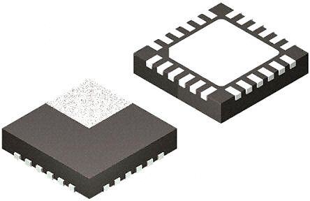
| 描述 | RF AMP 100MHZ DUAL VGA 24QFN |
| 产品分类 | RF 放大器 |
| 品牌 | Hittite Microwave Corporation |
| 数据手册 | 点击此处下载产品Datasheet |
| 产品图片 |  |
| P1dB | - |
| 产品型号 | HMC960LP4E |
| RF类型 | 通用 |
| rohs | 无铅 / 符合限制有害物质指令(RoHS)规范要求 |
| 产品系列 | - |
| 供应商器件封装 | 24-QFN(4x4) |
| 其它名称 | 1127-1195-6 |
| 包装 | Digi-Reel® |
| 噪声系数 | 6dB |
| 增益 | 40dB |
| 封装/外壳 | 24-VQFN 裸露焊盘 |
| 标准包装 | 1 |
| 测试频率 | - |
| 特色产品 | http://www.digikey.cn/product-highlights/zh/if-baseband-processing/52280 |
| 电压-电源 | 4.5 V ~ 5.5 V |
| 电流-电源 | 70mA |
| 频率 | 0Hz ~ 100MHz |
Datasheet
PDF Datasheet 数据手册内容提取
HMC960LP4E v01.1212 DC - 100 MHz DUAL DigitAL VAriAbLe gAin AMpLifier with DriVer typical Applications features The HMC960LP4E is suitable for: Low Noise: 6 dB NF • Baseband I/Q Transceivers High Linearity: Output IP3 +30 dBm • Direct Conversion & Low IF Transceivers Variable Gain: 0 to 40 dB • Diversity Receivers High Bandwidth: DC to 100 MHz • ADC Drivers Precise Gain Accuracy: 0.5 dB Gain Step • Adaptive Gain Control Excellent Magnitude and Phase Response Externally Controlled Common Mode Output Level Parallel or Serial Gain Control Read/Write Serial Port Interface (SPI) 24 Lead 4x4 mm SMT Package 16 mm2 Programmable Input Impedance (400 Ω Differential or 100 Ω Differential) T M S functional Diagram general Description - G The HMC960LP4E is a digitally programmable dual channel variable gain amplifier. It supports discrete N gain steps from 0 to 40 dB in precise 0.5 dB steps. I S It features a glitch free architecture to provide S exceptionally smooth gain transitions. The device E has matched gain paths which provide excellent C quadrature balance over a wide signal bandwidth. O The HMC960LP4E provides an SPI programmable R input impedance of 100 Ω differential or 400 Ω differential (default). P Externally controlled common mode output feature D enables the HMC960LP4E to provide a flexible output N interface to other parts in the signal path. A Gain can be controlled via either a parallel interface B (GC[6:0]) or via the read/write serial port (SPI). E S Housed in a compact 4x4mm (LP4) SMT QFN A package, the HMC960LP4E requires minimal external B components and provides a low cost alternative to more complicated switched amplifier architectures. / F I InfoFrmoarti opn rfuicrneish, edd eblyi vAenarlyog aDnevdic etso i sp blaelicevee do trod bee rasc:c uHraitet tiatned Mreliiacblreo. wHoawveveer ,C noo rpFoorra ptiroicne,, 2de Elivliezray,b aentdh tDo rpilvaece, Corhdeerlms: sAfnoarldog, MDeAv ic0e1s8, 2In4c., responsibility is assumed by Analog Devices for its use, nor for any infringements of patents or other One Technology Way, P.O. Box 9106, Norwood, MA 02062-9106 1 rliicgehntss eo fi sth girrda nptaerdti ebsy t himatp mlicaayt iorens 9uol7rt of8rtoh-me2r wit5sis 0ues -eu3.n dS3ep4re ca3infi yct aeptiaolt ne sn• ts ou rb9 jpe7act8te tno-t 2 crhi5gah0ntgs- e3o wf 3Ait7hnoa3ulot gfn aoDtixecve i .c •eNs o. OrPdheonr eO: 7n8-1l-in32e9 -a4t7 w00w (cid:127) wO.rhdeitrt iotnel.inceo amt www.analog.com Trademarks and registered trademarks are the property of their rAesppepcltiivce aowtinoerns. Support: appsA@pphliicttaittieon.c Soumpport: Phone: 1-800-ANALOG-D
HMC960LP4E v01.1212 DC - 100 MHz DUAL DigitAL VAriAbLe gAin AMpLifier with DriVer table 1. electrical Specifications T = +25°C, VDDI, VDDQ, DVDD = 5V +/-10%, GND = 0V, 400 Ω differential load unless otherwise stated. A Parameter Conditions Min. Typ. Max. Units Analog Performance Gain Range 0 40 dB Gain Step Size 0.5 dB Gain Step Error f = 40 MHz 0.05 ±0.2 dB Gain Absolute Error f = 40 MHz 0.1 ±0.2 dB DC Offset [4] measured over all gain settings 0 ±50 mV Signal Bandwidth 0.5 dB bandwidth over all gain settings 50 90 MHz 3 dB bandwidth 100 180 MHz Noise Figure Gain: 100 Ω Input Impedance (100 Ohm source) 0 dB (min gain) 23 dB 10 dB 14 dB 20 dB 7.5 dB 30 dB 6.5 dB 40 dB (max gain) 6 dB T 400 Ω Input Impedance (400 Ohm source) 0 dB (min gain) 17.5 dB M 10 dB 11 dB S 20 dB 6.7 dB 30 dB 6.3 dB - 40 dB (max gain) 6.1 dB G Output noise measured at f = 1 MHz N 0 dB gain 100 Ω matched input load 9 nV/rtHz 40 dB gain 125 nV/rtHz I S Output IP3 using two tones near 20 MHz S 0 dB gain at 2 Vppd output 32 dBm E 40 dB gain 33 dBm C IM3 using two tones near 20 MHz O 0 dB gain at 2 Vppd output -75 dBc 40 dB gain -80 dBc R Output IP2 using two tones near 20 MHz P 0 dB gain at 2 Vppd output 73 dBm 40 dB gain 73 dBm D IM2 using two tones near 20 MHz N 0 dB gain at 2 Vppd output -80 dBc A 40 dB gain -80 dBc B Sideband Suppression (Uncalibrated)[1] tested at 20 MHz over all gains 40 55 dB E I/Q Channel Balance[1] tested at 20 MHz S Gain 0.02 dB A Phase 0.15 degrees B I/Q Channel Isolation 60 70 dB / F Analog I/O I 100 Ω Mode 80 100 120 Ω Differential input impedance 400 Ω Mode 320 400 480 Ω Full Scale Differential Input min / max gain setting 2/0.02 Vppd 400 Ω Differential Load min / max gain setting 1/0.02 Vppd 100 Ω Differential Load Input Common Mode Voltage Range 1 4 V InfoFrmoarti opn rfuicrneis,h edd eblyi vAenarlyog aDnevdic etso isp blaelicevee do trod bee rasc:c uHraitett iatned Mreliiacblreo. wHoawveveer ,C noo rpFoorra ptiroicne,, 2d eElivliezray,b aentdh tDo rpilvaec,e Corhdeerlms: sAfnoarldog, MDeAv ic0e1s8, 2In4c., responsibility is assumed by Analog Devices for its use, nor for any infringements of patents or other One Technology Way, P.O. Box 9106, Norwood, MA 02062-9106 rights of third parties that may res9ul7t f8ro-m2 i5ts 0us-e3. S3p4ec3if ictaetiol n s• s u b9je7c8t to- 2ch5a0ng-e3 w3it7ho3ut fnaotxice . •N o OrPdheonr eO: 7n8-1l-in32e9 a-4t7 w00w (cid:127) wO.rhdeitrt iotnel.inceo amt www.analog.com 2 license is granted by implication or otherwise under any patent or patent rights of Analog Devices. Trademarks and registered trademarks are the property of their Aresppepcltiivce aowtinoerns. Support: appsA@pphliicttaittieon.c Soumpport: Phone: 1-800-ANALOG-D
HMC960LP4E v01.1212 DC - 100 MHz DUAL DigitAL VAriAbLe gAin AMpLifier with DriVer table 1. electrical Specifications, t = +25°C (Continued) A Parameter Conditions Min. Typ. Max. Units Full Scale Differential Output 400 Ω Differential Load 2 Vppd 100 Ω Differential Load 1 Vppd Output Voltage Range 0.5 Vdd - 0.5 V Output Common Mode Voltage Range [2] 1 Vdd/2 3 V Digital I/O Tested at 30 MHz Operation Logic Levels Digital Input Low Level (VIL) 0.4 V Digital Input High Level (VIH) 1.5 V Digital Output Low Level (VOL) 0.4 V Digital Output High Level (VOH) Vdd - 0.4 V Supply Related Digital I/O T Power Supply Analog & Digital Supplies 4.5 5 5.5 V M Supply Current [3] Both I/Q channels 70 mA S [1] Sideband Rejection is only measured in dB, but relates to phase/magnitude channel imbalance as follows, for a mismatch of 1 degree phase and - 0.1 dB magnitude: G SBR = -10Log[(1+A^2-2Acosx)/(1+A^2+2Acosx)] N where A = 10^(0.1/20) (linear magnitude) and x = 1*pi/180 (radians) [2] Output common mode voltage range is specified for worst case temperature, supply voltage, and bias settings with 2 Vppd signal amplitude. For SI 5 V supply and recommended biasing (op-amp bias =1 and driver bias=2), over 3.5 V is typical. See “Output IP3 vs. Common Mode Voltage vs. Driver Bias Setting[1]” in Figure 12 S [3] Recommend bias setting (op-amp bias =1 and driver bias=2) E [4] Standard deviation = 15 mV C table 2. test Conditions O R Unless otherwise specified, the following test conditions were used P Parameter Condition Temperature +27 °C D Gain Setting 0 dB N Output Signal Level 2 Vppd A Input/Output Common Mode Level 2.5 V B Programmed Impedance 200 Ω per input (400 Ω differential) E S Output Load 200 Ω per output (400 Ω differ- ential) A Supplies Analog: +5 V, Digital +5 V B / Driver Bias Setting ‘10’ F Op-Amp Bias Setting ‘01’ (Standard Setting) I InfoFrmoarti opn rfiucrneis,h edd eblyi vAenarlyog a Dnedvic etos isp blaelcievee do trod bee rasc:c uHraittet iatned Mreliiacbrleo. wHoawvevee r,C noo rpFoorra ptiroicne,, 2d eElivliezray,b aentdh tDo rpivlaec,e Corhdeelrms: sAfnoarldog, MDeAv ic0e1s8, 2In4c., responsibility is assumed by Analog Devices for its use, nor for any infringements of patents or other One Technology Way, P.O. Box 9106, Norwood, MA 02062-9106 3 rliicgehntss eo fi sth girrda nptaerdti ebsy t himatp mlicaayt iorens9 uo7lrt 8ofrtoh-me2r wi5tsis 0ues -eu3.n d3Sep4re c3ainf iyct aeptialo tne sn• ts ou 9rb jpe7ac8tte t-not2 cr5higah0ntgs- e3o wf3 Ait7hnoa3ulo t gfn aoDtxiecv ei .c •eN so . OrPdheorn eO: 7n8-1li-n32e9 a-4t7 w00w (cid:127)w O.rhdietrt iotenl.inceo amt www.analog.com Trademarks and registered trademarks are the property of their Arespppecltiivcea owtinoenrs. Support: appsA@pphliitctaittieo.nc Soumpport: Phone: 1-800-ANALOG-D
HMC960LP4E v01.1212 DC - 100 MHz DUAL DigitAL VAriAbLe gAin AMpLifier with DriVer figure 2. gain error, figure 1. gain vs. temperature (40 MHz) Absolute & Step (40 MHz) 40 0.1 35 30 0.05 AIN (dB)25 OR (dB) G20 R 0 ASURED 15 GAIN ER ME10 -0.05 27 C 85 C ABSOLUTE GAIN 5 -40 C RELATIVE GAIN 0 -0.1 0 5 10 15 20 25 30 35 40 0 5 10 15 20 25 30 35 40 PROGRAMMED GAIN (dB) PROGRAMMED GAIN (dB) figure 4. gain error, figure 3. gain vs. temperature (100 MHz) Absolute & Step (100 MHz) T 40 0.5 M 35 S 30 0.25 - AIN (dB)25 OR (dB) G G20 R 0 N ASURED 15 GAIN ER SI ME10 27 C -0.25 S 85 C 5 -40 C ABSOLUTE GAIN E RELATIVE GAIN C 0 -0.5 0 5 10 15 20 25 30 35 40 0 5 10 15 20 25 30 35 40 O PROGRAMMED GAIN (dB) PROGRAMMED GAIN (dB) R P D figure 5. frequency response vs. gain [1] figure 6. Channel isolation vs. gain [2] N A 50 -20 40dB GAIN B 40 -30 0dB 10dB E 20dB 30 -40 3400ddBB S 20 Bfs)-50 A d B GAIN (dB)100 0dB GAIN OLATION (--7600 0 dB Gain IF/ S -10 I-80 -20 -90 40 dB Gain -30 -100 0.1 1 10 100 1000 0.1 1 10 100 1000 FREQUENCY (MHz) FREQUENCY (MHz) [1] 2 dB Gain step increments [2] 10 dB Gain step increments InfoFrmoarti opn rfuicrneis,h edd eblyi vAenarlyog aDnevdic etso isp blaelicevee do trod bee rasc:c uHraitett iatned Mreliiacblreo. wHoawveveer ,C noo rpFoorra ptiroicne,, 2d eElivliezray,b aentdh tDo rpilvaec,e Corhdeerlms: sAfnoarldog, MDeAv ic0e1s8, 2In4c., responsibility is assumed by Analog Devices for its use, nor for any infringements of patents or other One Technology Way, P.O. Box 9106, Norwood, MA 02062-9106 rights of third parties that may res9ul7t f8ro-m2 i5ts 0us-e3. S3p4ec3if ictaetiol n s• s u b9je7c8t to- 2ch5a0ng-e3 w3it7ho3ut fnaotxice . •N o OrPdheonr eO: 7n8-1l-in32e9 a-4t7 w00w (cid:127) wO.rhdeitrt iotnel.inceo amt www.analog.com 4 license is granted by implication or otherwise under any patent or patent rights of Analog Devices. Trademarks and registered trademarks are the property of their Aresppepcltiivce aowtinoerns. Support: appsA@pphliicttaittieon.c Soumpport: Phone: 1-800-ANALOG-D
HMC960LP4E v01.1212 DC - 100 MHz DUAL DigitAL VAriAbLe gAin AMpLifier with DriVer figure 8. Output ip2 vs. figure 7. iM2 vs. frequency & gain [4] frequency & gain [4] -95 110 0 dB 100 10 dB 20 dB -100 30 dB 40 dB 90 IM2 (dBc)-105 01234 0000d BddddBBBB OIP2 (dBm)80 -110 70 -115 60 10 20 30 40 50 60 70 80 10 20 30 40 50 60 70 80 FREQUENCY (MHz) FREQUENCY (MHz) figure 9. iM3 vs. frequency and gain, figure 10. iM3 vs. frequency & gain, T Standard bias Setting [5][7] High Linearity bias Setting [6][7] M -40 -40 S -50 051dd0BBdB GLeasins STheattnin g3s0 dB -50 051dd0BBdB Gain Settings - 15dB 20dB Less Than 30 dB G -60 2205ddBB -60 1255ddBB SIN IM3 (dBc)--8700 334050dddBBB G 3a0i nd BS eotrt iGngresater IM3 (dBc)--8700 334050dddBBB Gain Settings S 30 dB or Greater E -90 -90 C -100 O -100 10 100 10 100 FREQUENCY (MHz) R FREQUENCY (MHz) P D figure 11. Output ip3 vs. frequency & figure 12. Output ip3 vs. frequency & N gain, Standard bias Setting [5] [7] gain, High Linearity bias Setting [6] [7] A 45 45 B E 40 40 Greater Than 30 dB S Gain Setting 35 Greater Than 30 dB 35 A Gain Setting IF/B OIP3 (dBm) 223050 051122dd0505BBddddBBBB OIP3 (dBm)223050 0511223dd05050BBdddddBBBBB LGeasins TSheattnin 3g0 dB 334050dddBBB LGeasins TSheattnin 3g0 dB 15 3450ddBB 15 10 10 10 100 10 100 FREQUENCY (MHz) FREQUENCY (MHz) [3] VGA Gain = 0 dB, 2 Vpp differential output [4] 300 mVppd output, load impedance = 400 Ω differential [5] Amplifier bias setting = ‘01’ (Standard Setting) [6] Amplifier bias setting = ‘10’ (High Linearity Setting) InfoFrmoarti opn rfiucrneis,h edd eblyi vAenarlyog a Dnedvic etos isp blaelcievee do trod bee rasc:c uHraittet iatned Mreliiacbrleo. wHoawvevee r,C noo rpFoorra ptiroicne,, 2d eElivliezray,b aentdh tDo rpivlaec,e Corhdeelrms: sAfnoarldog, MDeAv ic0e1s8, 2In4c., responsibility is assumed by Analog Devices for its use, nor for any infringements of patents or other One Technology Way, P.O. Box 9106, Norwood, MA 02062-9106 5 rliicgehntss eo fi sth girrda nptaerdti ebsy t himatp mlicaayt iorens9 uo7lrt 8ofrtoh-me2r wi5tsis 0ues -eu3.n d3Sep4re c3ainf iyct aeptialo tne sn• ts ou 9rb jpe7ac8tte t-not2 cr5higah0ntgs- e3o wf3 Ait7hnoa3ulo t gfn aoDtxiecv ei .c •eN so . OrPdheorn eO: 7n8-1li-n32e9 a-4t7 w00w (cid:127)w O.rhdietrt iotenl.inceo amt www.analog.com Trademarks and registered trademarks are the property of their Arespppecltiivcea owtinoenrs. Support: appsA@pphliitctaittieo.nc Soumpport: Phone: 1-800-ANALOG-D
HMC960LP4E v01.1212 DC - 100 MHz DUAL DigitAL VAriAbLe gAin AMpLifier with DriVer figure 13. Output ip3 vs. figure 14. Output ip3 vs. frequency & bias, gain = 10 db [5][6] [7] [9] frequency & bias, gain = 30 db [5][6] [7] [9] 45 45 40 40 35 35 m)30 m)30 B B d d P3 (25 P3 (25 OI OI Standard Bias Setting 20 20 High Linearity Bias Setting Standard Bias Setting 15 Hight Linearity Bias Setting 15 10 10 10 100 10 100 FREQUENCY (MHz) FREQUENCY (MHz) figure 15. Output ip3 vs. Output Common figure 16. Output ip3 vs. Output Common Mode, Standard bias Setting [3][5] Mode, High Linearity bias Settings [3][6] T 36 36 M S 34 34 - 32 32 G m) m) B B N P3 (d 30 P3 (d 30 4.5 V 5.5 V I OI Vdd = 4.5 4.5 V 5.5 V OI Vdd = 4.5 S Vdd = 4.75 Vdd = 4.75 Vdd = 5 Vdd = 5 S 28 VVdddd == 55..255 28 VVdddd == 55..255 E C 26 26 0.5 1 1.5 2 2.5 3 3.5 4 0.5 1 1.5 2 2.5 3 3.5 4 4.5 O COMMON MODE VOLTAGE (V) COMMON MODE VOLTAGE (V) R P figure 17. Output Voltage vs. figure 18. Output vs. D N input Voltage for Various gains expected Output Over gain [8] A 18 10 16 B 14 05ddBB 40 dB Gain E T VOLTAGE (Vppd) 1 40 dB Gain PUT POWER (dBm) 110246802 1122334re0505050fdddddddPBBBBBBB1dB 2Vppd / 1dBm 0 dB Gain F/BAS OUTPU 05112dd050BBdddBBB OUT --42 1Vppd / -5dBm I 25dB -6 30dB 0 dB Gain 3450ddBB -8 0.1 0.01 0.1 1 10 -10-10 -8 -6 -4 -2 0 2 4 6 8 10 12 14 16 18 20 INPUT VOLTAGE (Vppd) EXPECTED OUTPUT POWER (dBm) [7] Load Impedance = 400 Ω differential, 2 Vppd output [8] Output Power (dBm) is measured into 400 Ω output load [9] Use the following formulas conversion between dBm, dBV , and V , using a 400 Ω differential load: dBV = 20log(Vppd/2.8284), rms ppd rms dBm = 10log((Vppd/2.8284)2/400x10-3), dBm = dBV - 10log(400x10-3) rms InfoFrmoarti opn rfuicrneis,h edd eblyi vAenarlyog aDnevdic etso isp blaelicevee do trod bee rasc:c uHraitett iatned Mreliiacblreo. wHoawveveer ,C noo rpFoorra ptiroicne,, 2d eElivliezray,b aentdh tDo rpilvaec,e Corhdeerlms: sAfnoarldog, MDeAv ic0e1s8, 2In4c., responsibility is assumed by Analog Devices for its use, nor for any infringements of patents or other One Technology Way, P.O. Box 9106, Norwood, MA 02062-9106 rights of third parties that may res9ul7t f8ro-m2 i5ts 0us-e3. S3p4ec3if ictaetiol n s• s u b9je7c8t to- 2ch5a0ng-e3 w3it7ho3ut fnaotxice . •N o OrPdheonr eO: 7n8-1l-in32e9 a-4t7 w00w (cid:127) wO.rhdeitrt iotnel.inceo amt www.analog.com 6 license is granted by implication or otherwise under any patent or patent rights of Analog Devices. Trademarks and registered trademarks are the property of their Aresppepcltiivce aowtinoerns. Support: appsA@pphliicttaittieon.c Soumpport: Phone: 1-800-ANALOG-D
HMC960LP4E v01.1212 DC - 100 MHz DUAL DigitAL VAriAbLe gAin AMpLifier with DriVer figure 19. Output noise vs. Low figure 20. noise figure vs. frequency, 100 Ω rin [10] gain & input impedance at 1 MHz 1000 25 400 Ohm 20 100 Ohm E (nv/rtHz)100 40 dB Gain GURE (dB)15 OIS E FI N S OI10 N 10 0 dB Gain 5 0.001 0.01 0.1 1 10 100 0 5 10 15 20 25 30 35 40 FREQUENCY (MHz) PROGRAMMED GAIN (dB) figure 22. transient behavior, figure 21. Sideband rejection vs. gain 10 MHz, 6 db gain increase T M 75 0.4 6 dB gain increase S 70 1 MHz 0.3 dBc) 40 MHz 0.2 - ON ( 65 G TI V) 0.1 SIN BAND REJEC 5650 OUTPUT (-0.10 E S SID -0.2 E 50 -0.3 C 45 -0.4 O 0 5 10 15 20 25 30 35 40 4000 4500 5000 5500 6000 PROGRAMMED GAIN (dB) TIME (nsec) R P D N A B E S A B / F I [10] 5 dB Gain step increments InfoFrmoarti opn rfiucrneis,h edd eblyi vAenarlyog a Dnedvic etos isp blaelcievee do trod bee rasc:c uHraittet iatned Mreliiacbrleo. wHoawvevee r,C noo rpFoorra ptiroicne,, 2d eElivliezray,b aentdh tDo rpivlaec,e Corhdeelrms: sAfnoarldog, MDeAv ic0e1s8, 2In4c., responsibility is assumed by Analog Devices for its use, nor for any infringements of patents or other One Technology Way, P.O. Box 9106, Norwood, MA 02062-9106 7 rliicgehntss eo fi sth girrda nptaerdti ebsy t himatp mlicaayt iorens9 uo7lrt 8ofrtoh-me2r wi5tsis 0ues -eu3.n d3Sep4re c3ainf iyct aeptialo tne sn• ts ou 9rb jpe7ac8tte t-not2 cr5higah0ntgs- e3o wf3 Ait7hnoa3ulo t gfn aoDtxiecv ei .c •eN so . OrPdheorn eO: 7n8-1li-n32e9 a-4t7 w00w (cid:127)w O.rhdietrt iotenl.inceo amt www.analog.com Trademarks and registered trademarks are the property of their Arespppecltiivcea owtinoenrs. Support: appsA@pphliitctaittieo.nc Soumpport: Phone: 1-800-ANALOG-D
HMC960LP4E v01.1212 DC - 100 MHz DUAL DigitAL VAriAbLe gAin AMpLifier with DriVer table 3. Absolute Maximum ratings Nominal 5 V Supply to GND Reflow Soldering -0.3 to 5.5 V VDDI, VDDQ, DVDD Peak Temperature 260 °C Time at Peak Temperature 40 µs Common Mode Inputs Pins -0.3 to 5.5 V (CMI, CMQ) ESD Sensitivity (HBM) 1 kV Class 1 C Input and Output Pins IIP, IIN, IQP, IQN, OIP, OIN, OQP, -0.3 to 5.5 V Stresses above those listed under Absolute Maximum Ratings may OQN cause permanent damage to the device. This is a stress rating only; functional operation of the device at these or any other conditions Digital Pins above those indicated in the operational section of this specification SEN, SDI, SCK, SDO, GC[6:0] -0.3 to 5.5 V is not implied. Exposure to absolute maximum rating conditions for SDO min load impedance 1 kΩ extended periods may affect device reliability. Operating Temperature Range -40 to +85 °C Storage Temperature -65 to +125 °C Maximum Junction Temperature 125 °C ELECTROSTATIC SENSITIVE DEVICE Thermal Resistance (Rth) OBSERVE HANDLING PRECAUTIONS (junction to ground paddle) 10 °C/W T Outline Drawing M S - G N I S S E C O R P D N A NOTES: [1] PACKAGE BODY MATERIAL: LOW STRESS INJECTION MOLDED PLASTIC B SILICA AND SILICON IMPREGNATED. [2] LEAD AND GROUND PADDLE MATERIAL: COPPER ALLOY. E [3] LEAD AND GROUND PADDLE PLATING: 100% MATTE TIN. S [4] DIMENSIONS ARE IN INCHES [MILLIMETERS]. [5] LEAD SPACING TOLERANCE IS NON-CUMULATIVE. A [6] PAD BURR LENGTH SHALL BE 0.15mm MAX. PAD BURR HEIGHT SHALL BE 0.25m MAX. B [7] PACKAGE WARP SHALL NOT EXCEED 0.05mm / [8] ALL GROUND LEADS AND GROUND PADDLE MUST BE SOLDERED TO F PCB RF GROUND. [9] REFER TO HITTITE APPLICATION NOTE FOR SUGGESTED PCB LAND I PATTERN. package information Part Number Package Body Material Lead Finish MSL Rating [2] Package Marking [1] H960 HMC960LP4E RoHS-compliant Low Stress Injection Molded Plastic 100% matte Sn MSL1 XXXX [1] 4-Digit lot number XXXX [2] Max peak reflow temperature of 260 °C InfoFrmoarti opn rfuicrneis,h edd eblyi vAenarlyog aDnevdic etso isp blaelicevee do trod bee rasc:c uHraitett iatned Mreliiacblreo. wHoawveveer ,C noo rpFoorra ptiroicne,, 2d eElivliezray,b aentdh tDo rpilvaec,e Corhdeerlms: sAfnoarldog, MDeAv ic0e1s8, 2In4c., responsibility is assumed by Analog Devices for its use, nor for any infringements of patents or other One Technology Way, P.O. Box 9106, Norwood, MA 02062-9106 rights of third parties that may res9ul7t f8ro-m2 i5ts 0us-e3. S3p4ec3if ictaetiol n s• s u b9je7c8t to- 2ch5a0ng-e3 w3it7ho3ut fnaotxice . •N o OrPdheonr eO: 7n8-1l-in32e9 a-4t7 w00w (cid:127) wO.rhdeitrt iotnel.inceo amt www.analog.com 8 license is granted by implication or otherwise under any patent or patent rights of Analog Devices. Trademarks and registered trademarks are the property of their Aresppepcltiivce aowtinoerns. Support: appsA@pphliicttaittieon.c Soumpport: Phone: 1-800-ANALOG-D
HMC960LP4E v01.1212 DC - 100 MHz DUAL DigitAL VAriAbLe gAin AMpLifier with DriVer table 4. pin Descriptions Pin Number Function Description Interface Schematic 1 CMQ Quadrature (Q) channel output common mode level Quadrature (Q) channel positive and negative differential 2, 3 OQN, OQP outputs Gain Control Input Pins Gain is defined as: GC[6:0] = 0d —> Gain = 0 dB T GC[6:0] = 1d —> Gain = 0.5 dB 4 - 10 GC[6:0] M GC[6:0] = 2d —> Gain = 1 dB S GC[6:0] = 79d —> Gain = 39.5 dB GC[6:0] = 80d —> Gain = 40 dB - G 11 DVDD Digital 5V Supply. Must be locally decoupled to GND. N I S S 12, 14, 15 SCLK, SDI, SEN SPI Data clock, data input and enable respectively. E C O R P 13 SDO SPI Data Output D N A B E S Inphase (I) channel negative and positive differential A 16, 17 OIP, OIN outputs respectively B / F I 18 CMI Inphase (I) channel output common mode level InfoFrmoarti opn rfiucrneis,h edd eblyi vAenarlyog a Dnedvic etos isp blaelcievee do trod bee rasc:c uHraittet iatned Mreliiacbrleo. wHoawvevee r,C noo rpFoorra ptiroicne,, 2d eElivliezray,b aentdh tDo rpivlaec,e Corhdeelrms: sAfnoarldog, MDeAv ic0e1s8, 2In4c., responsibility is assumed by Analog Devices for its use, nor for any infringements of patents or other One Technology Way, P.O. Box 9106, Norwood, MA 02062-9106 9 rliicgehntss eo fi sth girrda nptaerdti ebsy t himatp mlicaayt iorens9 uo7lrt 8ofrtoh-me2r wi5tsis 0ues -eu3.n d3Sep4re c3ainf iyct aeptialo tne sn• ts ou 9rb jpe7ac8tte t-not2 cr5higah0ntgs- e3o wf3 Ait7hnoa3ulo t gfn aoDtxiecv ei .c •eN so . OrPdheorn eO: 7n8-1li-n32e9 a-4t7 w00w (cid:127)w O.rhdietrt iotenl.inceo amt www.analog.com Trademarks and registered trademarks are the property of their Arespppecltiivcea owtinoenrs. Support: appsA@pphliitctaittieo.nc Soumpport: Phone: 1-800-ANALOG-D
HMC960LP4E v01.1212 DC - 100 MHz DUAL DigitAL VAriAbLe gAin AMpLifier with DriVer table 4. pin Descriptions (Continued) Pin Number Function Description Interface Schematic Inphase (I) channel positive and negative differential 19, 20 IIP, IIN inputs respectively Inphase (I) Channel 5 V Supply. Must be locally decoupled 21 VDDI to GND Quadrature (Q) Channel 5 V Supply. Must be locally 22 VDDQ decoupled to GND Quadrature (Q) channel negative and positive differential 23, 24 IQN, IQP inputs respectively T M S - G N I S S E C O R P D N A B E S A B / F I InfoFrmoarti opn rfuicrneis,h edd eblyi vAenarlyog aDnevdic etso isp blaelicevee do trod bee rasc:c uHraitett iatned Mreliiacblreo. wHoawveveer ,C noo rpFoorra ptiroicne,, 2d eElivliezray,b aentdh tDo rpilvaec,e Corhdeerlms: sAfnoarldog, MDeAv ic0e1s8, 2In4c., responsibility is assumed by Analog Devices for its use, nor for any infringements of patents or other One Technology Way, P.O. Box 9106, Norwood, MA 02062-9106 rights of third parties that may res9ul7t f8ro-m2 i5ts 0us-e3. S3p4ec3if ictaetiol n s• s u b9je7c8t to- 2ch5a0ng-e3 w3it7ho3ut fnaotxice . •N o OrPdheonr eO: 7n8-1l-in32e9 a-4t7 w00w (cid:127) wO.rhdeitrt iotnel.inceo amt www.analog.com 10 license is granted by implication or otherwise under any patent or patent rights of Analog Devices. Trademarks and registered trademarks are the property of their Aresppepcltiivce aowtinoerns. Support: appsA@pphliicttaittieon.c Soumpport: Phone: 1-800-ANALOG-D
HMC960LP4E v01.1212 DC - 100 MHz DUAL DigitAL VAriAbLe gAin AMpLifier with DriVer evaluation pCb T M S - G N I S S E C O R The circuit board used in the application should use RF circuit design techniques. Signal lines should have 50 Ohms P impedance while the package ground leads and exposed paddle should be connected directly to the ground plane D similar to that shown. A sufficient number of via holes should be used to connect the top and bottom ground planes. The evaluation circuit board shown is available from Hittite upon request. N A B E S A B table 5. evaluation Order information / F Item Contents Part Number I Evaluation PCB Only HMC960LP4E Evaluation PCB 131109-HMC960LP4E HMC960LP4E Evaluation PCB USB Interface Board Evaluation Kit 131191-HMC960LP4E 6’ USB A Male to USB B Female Cable CD ROM (Contains User Manual, Evaluation PCB Schematic, Evaluation Software) InfoFrmoarti opn rfiucrneis,h edd eblyi vAenarlyog a Dnedvic etos isp blaelcievee do trod bee rasc:c uHraittet iatned Mreliiacbrleo. wHoawvevee r,C noo rpFoorra ptiroicne,, 2d eElivliezray,b aentdh tDo rpivlaec,e Corhdeelrms: sAfnoarldog, MDeAv ic0e1s8, 2In4c., responsibility is assumed by Analog Devices for its use, nor for any infringements of patents or other One Technology Way, P.O. Box 9106, Norwood, MA 02062-9106 11 rliicgehntss eo fi sth girrda nptaerdti ebsy t himatp mlicaayt iorens9 uo7lrt 8ofrtoh-me2r wi5tsis 0ues -eu3.n d3Sep4re c3ainf iyct aeptialo tne sn• ts ou 9rb jpe7ac8tte t-not2 cr5higah0ntgs- e3o wf3 Ait7hnoa3ulo t gfn aoDtxiecv ei .c •eN so . OrPdheorn eO: 7n8-1li-n32e9 a-4t7 w00w (cid:127)w O.rhdietrt iotenl.inceo amt www.analog.com Trademarks and registered trademarks are the property of their Arespppecltiivcea owtinoenrs. Support: appsA@pphliitctaittieo.nc Soumpport: Phone: 1-800-ANALOG-D
HMC960LP4E v01.1212 DC - 100 MHz DUAL DigitAL VAriAbLe gAin AMpLifier with DriVer evaluation Setup T M S HMC960Lp4e Application information - The wide bandwidth, large dynamic range, and excellent noise-linearity trade-off make the HMC960LP4E ideal for G Automatic Gain Control applications in the baseband section of a direct down-conversion receiver. Matched dual N amplifier design provides excellent gain and phase balance between the two channels. Externally controlled common I mode voltage, and SPI programmable input impedance simplify the interface between the HMC960LP4E and other S components in the signal path. The HMC960LP4E can be cascaded with HMC900LP5E without the need of any S matching circuitry. Together, these two components provide a complete baseband line-up that can directly drive E ADC’s such as the 12-bit, dual channel, 320 MSPS HMCAD1520. C O R P D N A B E S A B / F I Figure 1. Typical Receive Path Block Diagram Showing HMC960LP4E InfoFrmoarti opn rfuicrneis,h edd eblyi vAenarlyog aDnevdic etso isp blaelicevee do trod bee rasc:c uHraitett iatned Mreliiacblreo. wHoawveveer ,C noo rpFoorra ptiroicne,, 2d eElivliezray,b aentdh tDo rpilvaec,e Corhdeerlms: sAfnoarldog, MDeAv ic0e1s8, 2In4c., responsibility is assumed by Analog Devices for its use, nor for any infringements of patents or other One Technology Way, P.O. Box 9106, Norwood, MA 02062-9106 rights of third parties that may res9ul7t f8ro-m2 i5ts 0us-e3. S3p4ec3if ictaetiol n s• s u b9je7c8t to- 2ch5a0ng-e3 w3it7ho3ut fnaotxice . •N o OrPdheonr eO: 7n8-1l-in32e9 a-4t7 w00w (cid:127) wO.rhdeitrt iotnel.inceo amt www.analog.com 12 license is granted by implication or otherwise under any patent or patent rights of Analog Devices. Trademarks and registered trademarks are the property of their Aresppepcltiivce aowtinoerns. Support: appsA@pphliicttaittieon.c Soumpport: Phone: 1-800-ANALOG-D
HMC960LP4E v01.1212 DC - 100 MHz DUAL DigitAL VAriAbLe gAin AMpLifier with DriVer theory of Operation The HMC960LP4E consists of the following functional blocks 1. Input Match & Gain Stage 2. Second Gain Stage 3. Output Driver & Gain Stage 4. Bias Circuit 5. Serial Port Interface 6. Parallel Port Interface input Match & gain Stage The HMC960LP4E input stage consists of a user selectable 100 Ω or 400 Ω differential input impedance and a programmable gain of 0, 10 or 20 dB. A block diagram showing input impedance of the I channel is presented below, Q channel is similar. T M S - G N I S S E C O R P D N Figure 2. Input Stage Block Diagram A B E Second gain Stage S The HMC960LP4E second stage consists of a series of carefully scaled resistors to generate up to 10 dB of gain in 0.5 A dB steps. The gain step is fully determined by resistor ratios and as such the gain precision is relatively independent B of both temperature and process variation. / F I InfoFrmoarti opn rfiucrneis,h edd eblyi vAenarlyog a Dnedvic etos isp blaelcievee do trod bee rasc:c uHraittet iatned Mreliiacbrleo. wHoawvevee r,C noo rpFoorra ptiroicne,, 2d eElivliezray,b aentdh tDo rpivlaec,e Corhdeelrms: sAfnoarldog, MDeAv ic0e1s8, 2In4c., responsibility is assumed by Analog Devices for its use, nor for any infringements of patents or other One Technology Way, P.O. Box 9106, Norwood, MA 02062-9106 13 rliicgehntss eo fi sth girrda nptaerdti ebsy t himatp mlicaayt iorens9 uo7lrt 8ofrtoh-me2r wi5tsis 0ues -eu3.n d3Sep4re c3ainf iyct aeptialo tne sn• ts ou 9rb jpe7ac8tte t-not2 cr5higah0ntgs- e3o wf3 Ait7hnoa3ulo t gfn aoDtxiecv ei .c •eN so . OrPdheorn eO: 7n8-1li-n32e9 a-4t7 w00w (cid:127)w O.rhdietrt iotenl.inceo amt www.analog.com Trademarks and registered trademarks are the property of their Arespppecltiivcea owtinoenrs. Support: appsA@pphliitctaittieo.nc Soumpport: Phone: 1-800-ANALOG-D
HMC960LP4E v01.1212 DC - 100 MHz DUAL DigitAL VAriAbLe gAin AMpLifier with DriVer Output Driver & gain Stage The HMC960LP4E output driver consists of a differential class AB driver which is designed to drive typical ADC loads directly or can drive up to 200 Ω in parallel with 50 pF to AC ground per differential output. The stage provides a programmable 0 dB or 10 dB gain via switched resistors. Note that the output common mode of the driver is controlled directly via an input pin and can be set as per “Table 1. Electrical Specifications”. T M S - G N I S S E C Figure 3. Output Driver Block Diagram O R P D N A B E S A B / F I InfoFrmoarti opn rfuicrneis,h edd eblyi vAenarlyog aDnevdic etso isp blaelicevee do trod bee rasc:c uHraitett iatned Mreliiacblreo. wHoawveveer ,C noo rpFoorra ptiroicne,, 2d eElivliezray,b aentdh tDo rpilvaec,e Corhdeerlms: sAfnoarldog, MDeAv ic0e1s8, 2In4c., responsibility is assumed by Analog Devices for its use, nor for any infringements of patents or other One Technology Way, P.O. Box 9106, Norwood, MA 02062-9106 rights of third parties that may res9ul7t f8ro-m2 i5ts 0us-e3. S3p4ec3if ictaetiol n s• s u b9je7c8t to- 2ch5a0ng-e3 w3it7ho3ut fnaotxice . •N o OrPdheonr eO: 7n8-1l-in32e9 a-4t7 w00w (cid:127) wO.rhdeitrt iotnel.inceo amt www.analog.com 14 license is granted by implication or otherwise under any patent or patent rights of Analog Devices. Trademarks and registered trademarks are the property of their Aresppepcltiivce aowtinoerns. Support: appsA@pphliicttaittieon.c Soumpport: Phone: 1-800-ANALOG-D
HMC960LP4E v01.1212 DC - 100 MHz DUAL DigitAL VAriAbLe gAin AMpLifier with DriVer gain Decode Logic The decode logic automatically allocates gain to the three stages so as to minimize output noise and optimize noise figure. Without using decode logic gain can be allocated arbitrarily, as shown in Table 11. Decode logic gain allocation, shown in Figure 4, can be controlled via the parallel port or the SPI, and reflects gain control shown in Table 10. T M S - G N I S S E C O R P D N A B Figure 4. Decode Logic Gain Allocation E S A bias Circuit B A band gap reference circuit generates the reference currents used by the different sections. The bias circuit is / F enabled or disabled as required with the I or Q channel as appropriate. I InfoFrmoarti opn rfiucrneis,h edd eblyi vAenarlyog a Dnedvic etos isp blaelcievee do trod bee rasc:c uHraittet iatned Mreliiacbrleo. wHoawvevee r,C noo rpFoorra ptiroicne,, 2d eElivliezray,b aentdh tDo rpivlaec,e Corhdeelrms: sAfnoarldog, MDeAv ic0e1s8, 2In4c., responsibility is assumed by Analog Devices for its use, nor for any infringements of patents or other One Technology Way, P.O. Box 9106, Norwood, MA 02062-9106 15 rliicgehntss eo fi sth girrda nptaerdti ebsy t himatp mlicaayt iorens9 uo7lrt 8ofrtoh-me2r wi5tsis 0ues -eu3.n d3Sep4re c3ainf iyct aeptialo tne sn• ts ou 9rb jpe7ac8tte t-not2 cr5higah0ntgs- e3o wf3 Ait7hnoa3ulo t gfn aoDtxiecv ei .c •eN so . OrPdheorn eO: 7n8-1li-n32e9 a-4t7 w00w (cid:127)w O.rhdietrt iotenl.inceo amt www.analog.com Trademarks and registered trademarks are the property of their Arespppecltiivcea owtinoenrs. Support: appsA@pphliitctaittieo.nc Soumpport: Phone: 1-800-ANALOG-D
HMC960LP4E v01.1212 DC - 100 MHz DUAL DigitAL VAriAbLe gAin AMpLifier with DriVer Serial port interface The HMC960LP4E features a four wire serial port for simple communication with the host controller. Typical serial port operation can be run with SCK at speeds up to 30 MHz. The details of SPI access for the HMC960LP4E is provided in the following sections. Note that the READ operation below is always preceded by a WRITE operation to Register 0 to define the register to be queried. Also note that every READ cycle is also a WRITE cycle in that data sent to the SPI while reading the data will also be stored by the HMC960LP4E when SEN goes high. If this is not desired then it is suggested to write to Register 0 during the READ operation so that the status of the device will be unaffected. power on reset and Soft reset The HMC960LP4E has a built in Power On Reset (POR) and a serial port accessible Soft Reset (SR). POR is accomplished when power is cycled for the HMC960LP4E while SR is accomplished via the SPI by writing 20h to Reg 0h followed by writing 00h to Reg 0h. All chip registers will be reset to default states approximately 250 us after power up. Serial port Write Operation The host changes the data on the falling edge of SCK and the HMC960LP4E reads the data on the rising edge. T M A typical WRITE cycle is shown in Figure 5. It is 32 clock cycles long. S 1. The host both asserts SEN (active low Serial Port Enable) and places the MSB of the data on SDI followed by a rising edge on SCK. - G 2. HMC960LP4E reads SDI (the MSB) on the 1st rising edge of SCK after SEN. N 3. HMC960LP4E registers the data bits, D23:D0, in the next 23 rising edges of SCK (total of 24 data bits). I S 4. Host places the 5 register address bits, A4:A0, on the next 5 falling edges of SCK (MSB to LSB) while the HMC960LP4E reads the address bits on the corresponding rising edge of SCK. S E 5. Host places the 3 chip address bits, CA2:CA0=[110], on the next 3 falling edges of SCK (MSB to LSB). Note C the HMC960LP4E chip address is fixed as “6d” or “110b”. O 6. SEN goes from low to high after the 32th rising edge of SCK. This completes the WRITE cycle. R 7. HMC960LP4E also exports data back on the SDO line. For details see the section on READ operation. P D Serial port reAD Operation N The SPI can read from the internal registers in the chip. The data is available on SDO pin. This pin itself is tri-stated A when the device is not being addressed. However when the device is active and has been addressed by the SPI B master, the HMC960LP4E controls the SDO pin and exports data on this pin during the next SPI cycle. E HMC960LP4E changes the data to the host on the rising edge of SCK and the host reads the data from HMC960LP4E S on the falling edge. A B A typical READ cycle is shown in Figure 5. Read cycle is 32 clock cycles long. To specifically read a register, the / address of that register must be written to dedicated Reg 0h. This requires two full cycles, one to write the F required address, and a 2nd to retrieve the data. A read cycle can then be initiated as follows; I 1. The host asserts SEN (active low Serial Port Enable) followed by a rising edge SCK. 2. HMC960LP4E reads SDI (the MSB) on the 1st rising edge of SCK after SEN. 3. HMC960LP4E registers the data bits in the next 23 rising edges of SCK (total of 24 data bits). The LSBs of the data bits represent the address of the register that is intended to be read. 4. Host places the 5 register address bits on the next 5 falling edges of SCK (MSB to LSB) while the HMC960LP4E reads the address bits on the corresponding rising edge of SCK. For a read operation this is “00000”. InfoFrmoarti opn rfuicrneis,h edd eblyi vAenarlyog aDnevdic etso isp blaelicevee do trod bee rasc:c uHraitett iatned Mreliiacblreo. wHoawveveer ,C noo rpFoorra ptiroicne,, 2d eElivliezray,b aentdh tDo rpilvaec,e Corhdeerlms: sAfnoarldog, MDeAv ic0e1s8, 2In4c., responsibility is assumed by Analog Devices for its use, nor for any infringements of patents or other One Technology Way, P.O. Box 9106, Norwood, MA 02062-9106 rights of third parties that may res9ul7t f8ro-m2 i5ts 0us-e3. S3p4ec3if ictaetiol n s• s u b9je7c8t to- 2ch5a0ng-e3 w3it7ho3ut fnaotxice . •N o OrPdheonr eO: 7n8-1l-in32e9 a-4t7 w00w (cid:127) wO.rhdeitrt iotnel.inceo amt www.analog.com 16 license is granted by implication or otherwise under any patent or patent rights of Analog Devices. Trademarks and registered trademarks are the property of their Aresppepcltiivce aowtinoerns. Support: appsA@pphliicttaittieon.c Soumpport: Phone: 1-800-ANALOG-D
HMC960LP4E v01.1212 DC - 100 MHz DUAL DigitAL VAriAbLe gAin AMpLifier with DriVer 5. Host places the 3 chip address bits <110> on the next 3 falling edges of SCK (MSB to LSB). Note the HMC960LP4E chip address is fixed as “6d” or “110b”. 6. SEN goes from low to high after the 32nd rising edge of SCK. This completes the first portion of the READ cycle. 7. The host asserts SEN (active low Serial Port Enable) followed by a rising edge SCK. 8. HMC960LP4E places the 24 data bits, 5 address bits, and 3 chip id bits, on the SDO, on each rising edge of the SCK, commencing with the first rising edge beginning with MSB. 9. The host de-asserts SEN (i.e. sets SEN high) after reading the 32 bits from the SDO output. The 32 bits consists of 24 data bits, 5 address bits, and the 3 chip id bits. This completes the read cycle. Note that the data sent to the SPI during this portion of the READ operation is stored in the SPI when SEN is de-asserted. This can potentially change the state of the HMC960LP4E. If this is undesired it is recommended that during the second phase of the READ operation that Reg 0h is addressed with either the same address or the address of another register to be read during the next cycle. T M S - G N I S S E C O R P Figure 5. SPI Timing Diagram D N A B E S A B / F I InfoFrmoarti opn rfiucrneis,h edd eblyi vAenarlyog a Dnedvic etos isp blaelcievee do trod bee rasc:c uHraittet iatned Mreliiacbrleo. wHoawvevee r,C noo rpFoorra ptiroicne,, 2d eElivliezray,b aentdh tDo rpivlaec,e Corhdeelrms: sAfnoarldog, MDeAv ic0e1s8, 2In4c., responsibility is assumed by Analog Devices for its use, nor for any infringements of patents or other One Technology Way, P.O. Box 9106, Norwood, MA 02062-9106 17 rliicgehntss eo fi sth girrda nptaerdti ebsy t himatp mlicaayt iorens9 uo7lrt 8ofrtoh-me2r wi5tsis 0ues -eu3.n d3Sep4re c3ainf iyct aeptialo tne sn• ts ou 9rb jpe7ac8tte t-not2 cr5higah0ntgs- e3o wf3 Ait7hnoa3ulo t gfn aoDtxiecv ei .c •eN so . OrPdheorn eO: 7n8-1li-n32e9 a-4t7 w00w (cid:127)w O.rhdietrt iotenl.inceo amt www.analog.com Trademarks and registered trademarks are the property of their Arespppecltiivcea owtinoenrs. Support: appsA@pphliitctaittieo.nc Soumpport: Phone: 1-800-ANALOG-D
HMC960LP4E v01.1212 DC - 100 MHz DUAL DigitAL VAriAbLe gAin AMpLifier with DriVer DVDD = 5 V ±10%, GND = 0 V table 6. Main Spi timing Characteristics Parameter Conditions Min Typ Max Units t1 SDI to SCK Setup Time 8 nsec t2 SDI to SCK Hold Time 8 nsec t3 SCK High Duration [1] 10 nsec t4 SCK Low Duration 10 nsec t5 SEN Low Duration 20 nsec t6 SEN High Duration 20 nsec t7 SCK to SEN [2] 8 nsec t8 SCK to SDO out [3] 8 nsec [1] The SPI is relatively insensitive to the duty cycle of SCK. [2] SEN must rise after the 32nd falling edge of SCK but before the next rising SCK edge. If SCK is shared amongst several devices this timing must be respected. [3] Typical load to SDO is 10 pF, maximum 20 pF T M parallel port interface S The HMC960LP4E features a seven bit parallel port to aid in real time gain selection. The dynamic performance of - the parallel port is specified below. G N table 7. gain Control parallel port timing Characteristics I S Parameter Conditions Min. Typ. Max. Units S f Gain control switching rate 20 MHz E SSP C t Allowable skew between GC[6:0] input transitions 10 nsec SSP O R P D N A B E S A B / F I InfoFrmoarti opn rfuicrneis,h edd eblyi vAenarlyog aDnevdic etso isp blaelicevee do trod bee rasc:c uHraitett iatned Mreliiacblreo. wHoawveveer ,C noo rpFoorra ptiroicne,, 2d eElivliezray,b aentdh tDo rpilvaec,e Corhdeerlms: sAfnoarldog, MDeAv ic0e1s8, 2In4c., responsibility is assumed by Analog Devices for its use, nor for any infringements of patents or other One Technology Way, P.O. Box 9106, Norwood, MA 02062-9106 rights of third parties that may res9ul7t f8ro-m2 i5ts 0us-e3. S3p4ec3if ictaetiol n s• s u b9je7c8t to- 2ch5a0ng-e3 w3it7ho3ut fnaotxice . •N o OrPdheonr eO: 7n8-1l-in32e9 a-4t7 w00w (cid:127) wO.rhdeitrt iotnel.inceo amt www.analog.com 18 license is granted by implication or otherwise under any patent or patent rights of Analog Devices. Trademarks and registered trademarks are the property of their Aresppepcltiivce aowtinoerns. Support: appsA@pphliicttaittieon.c Soumpport: Phone: 1-800-ANALOG-D
HMC960LP4E v01.1212 DC - 100 MHz DUAL DigitAL VAriAbLe gAin AMpLifier with DriVer register Map Three registers provide all the required functionality via the SPI port. table 8. reg 01h - enable register Bit Name Width Default Description [0] VGA_I_enable 1 1 VGA I channel enable bit [1] VGA_Q_enable 1 1 VGA Q channel enable bit [2:3] spare 2 0 [23:4] unused 19 table 9. reg 02h - Settings register Bit Name Width Default Description T M Opamp bias setting. 00 -- min bias S [1:0] opamp_bias[1:0] 2 01 11 -- max bias opamp_bias[1:0]=01 recommended for low frequency operation or 10 for - improved linearity for higher frequency operation. G Driver bias setting. N 00 -- min bias [3:2] drvr_bias[1:0] 2 01 11 -- max bias I S drvr_bias[1:0]=10 recommended (characterized on recommended setting S only) E Input impedance setting: [4] Rin_50ohm_select 1 1 0: Rin of 200 ohms selected C 1: Rin of 50 ohms selected O Source of Gain Control Input R [5] Gain_Control_from_SPI 1 0 0: Gain control taken from parallel port (pins) P 1: Gain control taken from SPI register 3 Bypass gain decoder D 0: Decoded gain taken from register 3, bits <8:0> [6] Gain_Decode_Disable 1 0 N 1: Undecoded gain taken from register 3, bits <8:0> (SPI gain control must be selected) A B Bypass gain deglitcher 0: Gain control deglitching active E [7] Gain_Deglitching_Disable 1 0 1: Gain control deglitching disabled S (applies to SPI and parallel port gain control) A [23:8] unused B / F I InfoFrmoarti opn rfiucrneis,h edd eblyi vAenarlyog a Dnedvic etos isp blaelcievee do trod bee rasc:c uHraittet iatned Mreliiacbrleo. wHoawvevee r,C noo rpFoorra ptiroicne,, 2d eElivliezray,b aentdh tDo rpivlaec,e Corhdeelrms: sAfnoarldog, MDeAv ic0e1s8, 2In4c., responsibility is assumed by Analog Devices for its use, nor for any infringements of patents or other One Technology Way, P.O. Box 9106, Norwood, MA 02062-9106 19 rliicgehntss eo fi sth girrda nptaerdti ebsy t himatp mlicaayt iorens9 uo7lrt 8ofrtoh-me2r wi5tsis 0ues -eu3.n d3Sep4re c3ainf iyct aeptialo tne sn• ts ou 9rb jpe7ac8tte t-not2 cr5higah0ntgs- e3o wf3 Ait7hnoa3ulo t gfn aoDtxiecv ei .c •eN so . OrPdheorn eO: 7n8-1li-n32e9 a-4t7 w00w (cid:127)w O.rhdietrt iotenl.inceo amt www.analog.com Trademarks and registered trademarks are the property of their Arespppecltiivcea owtinoenrs. Support: appsA@pphliitctaittieo.nc Soumpport: Phone: 1-800-ANALOG-D
HMC960LP4E v01.1212 DC - 100 MHz DUAL DigitAL VAriAbLe gAin AMpLifier with DriVer table 10. reg 03h - gain Control register WHen USing decode logic [1][2] Bit Name Width Default Description Reg 02h[5]=1 and Reg 02h[6]=0 (i.e. SPI gain control & gain decode enabled) gain[6:0] defines teh VGA channel I and Q gain of 0-40dB as follows... 0000000 - 0 dB, minimum gain setting 0000001 - 0.5 dB gain 0000010 - 1.0 dB gain [6:0] gain[6:0] 7 0000000 ... 1001110 - 39 dB gain 1001111 - 39.5 dB gain 1010000 - 40 dB, maximum gain setting Reg 02h[5] = 1 and Reg 02h[6] = 1 (i.e. SPI gain control & gain decode bypassed) [23:7] unused T M S - table 11. reg 03h - gain Control register, WHen nOt using decode logic [3][4] G Bit Name Width Default Description N gain[8:0] define the VGA I and Q channel gain when Reg 02h[5] = 1 and I S Reg 02h[6] = 1 (i.e. SPI gain control and gain decode bypassed) S Generally the first 4 bits control the 1st and 3rd stage while the last 5 E bits control the 2nd stage gain. C x001nnnnn - 1st stage set to 0 dB x010nnnnn - 1st stage set to 10 dB O x100nnnnn - 1st stage set to 20 dB R [8:0] gain[8:0] 9 000000000 0xxxnnnnn - 3rd stage set to 0 dB P 1xxxnnnnn - 3rd stage set to 10 dB D xxxxnnnnn - 2nd stage set as follows: N nnnnn = 00000 - set to 0 dB A nnnnn = 00001 - set to 0.5 dB nnnnn = 10011 - set to 9.5 dB B nnnnn = 10100 - set to 10 dB E [23:9] unused S A B / F I [1] Reg 03h bit assignment depends on the setting of bits 5 and 6 in Reg 02h. If Reg 02h[5]=0, then all Reg 03h bits are ignored (parallel port selected) [2] For Reg 02h[5]=1 and Reg 02h[6]=0, gain control is via an SPI register with decode, and Reg 03h[6:0] are used as follows. [3] Note that the Parallel Port gain logic always uses the gain decode logic, and therefore the bit encoding is the same as Reg 03h - Gain Control Register WHEN USING decode logic. [4] For Reg 02h[5]=1 and Reg 02h[6]=1, gain control is via an SPI register without decode, and Reg 03h[6:0] are used as follows. InfoFrmoarti opn rfuicrneis,h edd eblyi vAenarlyog aDnevdic etso isp blaelicevee do trod bee rasc:c uHraitett iatned Mreliiacblreo. wHoawveveer ,C noo rpFoorra ptiroicne,, 2d eElivliezray,b aentdh tDo rpilvaec,e Corhdeerlms: sAfnoarldog, MDeAv ic0e1s8, 2In4c., responsibility is assumed by Analog Devices for its use, nor for any infringements of patents or other One Technology Way, P.O. Box 9106, Norwood, MA 02062-9106 rights of third parties that may res9ul7t f8ro-m2 i5ts 0us-e3. S3p4ec3if ictaetiol n s• s u b9je7c8t to- 2ch5a0ng-e3 w3it7ho3ut fnaotxice . •N o OrPdheonr eO: 7n8-1l-in32e9 a-4t7 w00w (cid:127) wO.rhdeitrt iotnel.inceo amt www.analog.com 20 license is granted by implication or otherwise under any patent or patent rights of Analog Devices. Trademarks and registered trademarks are the property of their Aresppepcltiivce aowtinoerns. Support: appsA@pphliicttaittieon.c Soumpport: Phone: 1-800-ANALOG-D