首页 > HMC921LP4E > 详情
 Datasheet下载
- 型号: HMC921LP4E
- 制造商: Hittite
- 库位|库存: xxxx|xxxx
- 要求:
| 数量阶梯 | 香港交货 | 国内含税 |
| +xxxx | $xxxx | ¥xxxx |
查看当月历史价格
查看今年历史价格
产品参数
| 参数 | 数值 |
| 产品目录 | 射频/IF 和 RFID |
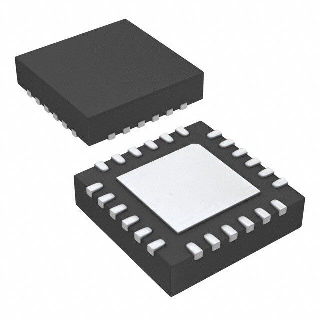
| 描述 | IC AMP MMIC GASS 24QFN |
| 产品分类 | RF 放大器 |
| 品牌 | Hittite Microwave Corporation |
| 数据手册 | 点击此处下载产品Datasheet |
| 产品图片 |  |
| P1dB | 33.3dB |
| 产品型号 | HMC921LP4E |
| RF类型 | 通用 |
| rohs | 无铅 / 符合限制有害物质指令(RoHS)规范要求 |
| 产品系列 | - |
| 供应商器件封装 | 24-QFN(4x4) |
| 其它名称 | 1127-1078-1 |
| 包装 | 剪切带 (CT) |
| 噪声系数 | 6.5dB |
| 增益 | 9dB |
| 封装/外壳 | 24-VQFN 裸露焊盘 |
| 标准包装 | 1 |
| 测试频率 | - |
| 电压-电源 | 5V |
| 电流-电源 | 400mA |
| 配用 | /product-detail/zh/131924-HMC921LP4E/1127-2253-ND/4794553/product-detail/zh/131907-HMC921LP4E/1127-2443-ND/4794734/product-detail/zh/131903-HMC921LP4E/1127-2778-ND/4863552 |
| 频率 | 400MHz ~ 2.7GHz |
Datasheet
PDF Datasheet 数据手册内容提取
HMC921LP4E v02.0312 GaAs HBT MMIC 2 WATT POWER AMPLIFIER, 0.4 - 2.7 GHz Typical Applications Features The HmC921lp4e is ideal for: High output ip3: +48 dBm T • Cellular/3G & WiMAX/LTE/4G High output p1dB: +33 dBm m • Fixed Wireless & WLAN High Gain: 16 dB @ 900 mHz s E • CATV, Cable Modem & DBS single supply: +5V - r • Microwave Radio & Test Equipment 32% pAe @ +33 dBm pout e • IF & RF Applications Adjustable Bias CurrentT w 24 lead 4x4 mm smT package: 16 mm² o p E Functional Diagram General Description & The HmC921lp4e is a high linearity GaAs HBT r mmiC 2 watt power amplifier operating from 0.4 to A L 2.7 GHz and is housed in a roHs compliant 4x4 mm e Qfn leadless package. The HmC921lp4e utilizes n a minimum number of external components and li O operates from a single +5V supply. This versatile - power amplifier can be biased for both low quiescent s current and high quiescent current modes by adjusting r a single external resistor. e S i f i l p B m A Electrical SpecifiOcations, T = +25°C, Vcc1 = Vcc2 = VEN = +5V [1] A 400 mA (r1 = 270 Ω) parameter min. Typ. max. min. Typ. max. min. Typ. max. min. Typ. max. min. Typ. max. Units frequency range 350 - 500 800 - 1000 1800 - 2000 2000 - 2200 2500 - 2800 mHz Gain 17 19 14 16 9 11 9.5 10.5 8 9 dB Gain Variation over Temperature 0.01 0.01 0.01 0.01 0.01 dB / °C input return loss 9 12 10 15 5 10 8 12 6 11 dB output return loss 6 10 5 9 8 9 6 7 9 10 dB output power for 1dB 32.5 34 30.5 32 31 32.5 32 32.5 33 33.3 dBm Compression (p1dB) saturated output power (psat) 35 34 34 34 34.5 dBm output Third order 47 44 43 43 45 dBm intercept (ip3) noise figure 12.9 9 8.5 6.9 6.5 dB supply Current (icq) ien 8 8 8 8 8 mA icc1 12 12 12 12 12 mA icc2 400 400 400 400 400 mA [1] specifications and data reflect HmC921lp4e measured using the respective application circuits for each designated frequency band found herein. Contact the HmC Applications Group for assistance in optimizing performance for your application. InfoFrmoart iopn rfiucrneis,h edde blyi vAenraylo ga Dnedvic teos ips lbaelcieeve do rtod beer sac:c Huraittet iatned Mreliiacbrleo. wHoawveeve rC, noo rpoForar tpioricne,, 2d eElilviezrayb, aentdh tDo rpivlaec,e C ohrdeelrms: sAfonardlo,g MDeAv i0ce1s8, 2In4c., responsibility is assumed by Analog Devices for its use, nor for any infringements of patents or other One Technology Way, P.O. Box 9106, Norwood, MA 02062-9106 1 rliicgehntss eo fi sth girrda nptaerdti ebsy t himatp mlicaaPyt iorhenso uonlrt ofertoh:m e9r wit7sis 8ues -eu2.n dS5ep0re ca-inf3iyc 3aptia4otne3sn ts ou rb jpeFacttae tnoxt c:r hig9ahn7tgs 8eo wf- 2Aithn5oau0lot g-n 3oDti3ecve7i.c 3eNso . POhrodnee:r 7 O81n-3-l2i9n-e4 7a0t0 w(cid:127) wOrwde.hr oitntliitnee. cato wmww.analog.com Trademarks and registered trademarks arAe tphep plriocpearttyi oof nth eSir urepsppecotivret :o wPnehrso.ne: 978-250-3A3p4p3li c aotrio na Spuppsp@orht: iPtthitoen.ec: o1-m800-ANALOG-D
HMC921LP4E v02.0312 GaAs HBT MMIC 2 WATT POWER AMPLIFIER, 0.4 - 2.7 GHz Electrical Specifications, T = +25°C, Vcc1 = Vcc2 = VEN = +5V [1] A 700 mA (r1 = 130 Ω) parameter min. Typ. max. min. Typ. max. min. Typ. max. min. Typ. max. min. Typ. max. Units T frequency range 350 - 500 800 - 1000 1800 - 2000 2000 - 2200 2600 - 2800 mHz m Gain 19 19.5 14 16 9 11 10.3 10.8 8 E9 dB s Gain Variation over Temperature 001 0.01 0.01 0.01 0.01 dB / °C - input return loss 9 12 11 15 6 10 9 13 6 12 dB r output return loss 6 10 6 9 8 9 6 7.5 9 10 dB e T output power for 1dB w 33 34.5 31 32.5 31.5 33 32.8 33.5 33 34 dBm Compression (p1dB) o saturated output power (psat) 35 34 34 34.5 35 dBm p output Third order E intercept (ip3) 43 45 46 47 47 dBm & noise figure 14 9 8.5 8 8 dB r supply Current (icq) ien 13 13 13 13 13 mA icc1 14 14 L14 14 14 mA A icc2 700 700 700 700 700 mA e [1] specifications and data reflect HmC921lp4e measured using the respective application circuits for each designated frequency band found n herein. Contact the HmC Applications Group for assistance in optimizing performance for your application. O li 450 MHz Tune - Broadband Gain & Return Loss @ 400mA Broadband Gain & Return Loss @ 700mA s r 20 20 S e 15 15 i 10 SS2111 10 SS2111 f E (dB) 5 S22B E (dB) 5 S22 pli S S ON 0 ON 0 m P P ES -5 ES -5 A R R -10 -10 O -15 -15 -20 -20 0.1 0.2 0.3 0.4 0.5 0.6 0.7 0.8 0.9 0.1 0.2 0.3 0.4 0.5 0.6 0.7 0.8 0.9 FREQUENCY (GHz) FREQUENCY (GHz) Gain vs. Temperature @ 400mA Gain vs. Temperature @ 700mA 20 20 18 18 16 16 B) B) N (d 14 N (d 14 AI AI G G +25 C 12 12 +85 C +25 C - 40 C +85 C 10 - 40 C 10 8 8 0.1 0.2 0.3 0.4 0.5 0.6 0.7 0.8 0.9 0.1 0.2 0.3 0.4 0.5 0.6 0.7 0.8 0.9 FREQUENCY (GHz) FREQUENCY (GHz) InfoFrmoart iopn rfiucrneis,h edde blyi vAenraylo ga Dnedvic teos ips lbaelcieeve do rtod beer sac:c Huraittet iatned Mreliiacbrleo. wHoawveeve rC, noo rpoForar tpioricne,, 2d eElilviezrayb, aentdh tDo rpivlaec,e C ohrdeelrms: sAfonardlo,g MDeAv i0ce1s8, 2In4c., responsibility is assumed by Analog Devices for its use, nor for any infringements of patents or other One Technology Way, P.O. Box 9106, Norwood, MA 02062-9106 rights of third parties that maPy rhesounlt fero:m 9 it7s 8us-e2. S5p0ec-if3ic3ati4on3s s u b jeFcta tox c: h9an7g8e w-2ith5ou0t -n3oti3ce7. 3No POhrodnee:r 7 O81n-3-l2i9n-e4 7a0t0 w(cid:127) wOrwde.hr oitntliitnee. cato wmww.analog.com 2 license is granted by implication or otherwise under any patent or patent rights of Analog Devices. Trademarks and registered trademarks arAe tphep plriocpearttyi oof nth eSir urepsppecotivret :o wPnehrso.ne: 978-250-3A3p4p3li c aotrio na Spuppsp@orht: iPtthitoen.ec: o1-m800-ANALOG-D
HMC921LP4E v02.0312 GaAs HBT MMIC 2 WATT POWER AMPLIFIER, 0.4 - 2.7 GHz 450 MHz Tune Input Return Loss @ 400 mA Input Return Loss @ 700 mA 0 0 T m -5 -5 B) B) s OSS (d-10 OSS (d-10 E - L L N N r UR-15 UR-15 T T e E E R R T w -20 ++2855 CC -20 ++2855 CC - 40 C - 40 C o -25 -25 p 0.3 0.4 0.5 0.6 0.7 0.3 E0.4 0.5 0.6 0.7 & FREQUENCY (GHz) FREQUENCY (GHz) r A L e Output return Loss @ 400 mA Output return Loss @ 700 mA n 0 0 li O - B) -5 B) -5 s S (d S (d r OS OS e N L-10 S N L-10 R R fi RETU +25 C RETU +25 C i -15 +85 C -15 +85 C l - 40 C - 40 C p B m -20 -20 0.1 0.2 0.3 0.4 0.5 0.6 0.7 0.8 0.9 0.1 0.2 0.3 0.4 0.5 0.6 0.7 0.8 0.9 A FREQUENCY (GHz) FREQUENCY (GHz) O P1dB vs. Temperature @ 400 mA P1dB vs. Temperature @ 700 mA 36 36 35 35 34 34 m) 33 m) 33 B B B (d 32 B (d 32 d d 1 1 P 31 +25 C P 31 +25 C +85 C +85 C 30 - 40 C 30 - 40 C 29 29 28 28 0.35 0.4 0.45 0.5 0.55 0.35 0.4 0.45 0.5 0.55 FREQUENCY (GHz) FREQUENCY (GHz) InfoFrmoart iopn rfiucrneis,h edde blyi vAenraylo ga Dnedvic teos ips lbaelcieeve do rtod beer sac:c Huraittet iatned Mreliiacbrleo. wHoawveeve rC, noo rpoForar tpioricne,, 2d eElilviezrayb, aentdh tDo rpivlaec,e C ohrdeelrms: sAfonardlo,g MDeAv i0ce1s8, 2In4c., responsibility is assumed by Analog Devices for its use, nor for any infringements of patents or other One Technology Way, P.O. Box 9106, Norwood, MA 02062-9106 3 rliicgehntss eo fi sth girrda nptaerdti ebsy t himatp mlicaaPyt iorhenso uonlrt ofertoh:m e9r wit7sis 8ues -eu2.n dS5ep0re ca-inf3iyc 3aptia4otne3sn ts ou rb jpeFacttae tnoxt c:r hig9ahn7tgs 8eo wf- 2Aithn5oau0lot g-n 3oDti3ecve7i.c 3eNso . POhrodnee:r 7 O81n-3-l2i9n-e4 7a0t0 w(cid:127) wOrwde.hr oitntliitnee. cato wmww.analog.com Trademarks and registered trademarks arAe tphep plriocpearttyi oof nth eSir urepsppecotivret :o wPnehrso.ne: 978-250-3A3p4p3li c aotrio na Spuppsp@orht: iPtthitoen.ec: o1-m800-ANALOG-D
HMC921LP4E v02.0312 GaAs HBT MMIC 2 WATT POWER AMPLIFIER, 0.4 - 2.7 GHz 450 MHz Tune Psat vs. Temperature @ 400mA Psat vs. Temperature @ 700mA 36 36 35 35 T m 34 34 m) m) E s B 33 B 33 Psat (d 32 +25 C Psat (d 32 +25 C r - +85 C +85 C 31 - 40 C 31 T- 40 C e w 30 30 o 29 29 p 0.35 0.4 0.45 0.5 0.55 0.35 E0.4 0.45 0.5 0.55 FREQUENCY (GHz) FREQUENCY (GHz) & r L A Output IP3 vs. Output Power @ 400mA Output IP3 vs. Output Power @ 700mA e n 55 55 O li +25 C 50 50 +85 C - - 40 C s B) B) r d d P3 ( 45 S P3 ( 45 e I I i f +25 C 40 +85 C 40 i - 40 C l B p 35 35 m 20 21 22 23 24 25 26 27 28 29 20 21 22 23 24 25 26 27 28 29 A SINGLE TONE POUT (dBm) SINGLE TONE POUT (dBm) O Noise Figure vs. Temperature @ 400mA Noise Figure vs. Temperature @ 700mA 18 18 16 B) B) 16 d d RE ( 14 RE ( U U G G 14 FI FI E 12 E S S OI OI N +25 C N 12 ++2855 CC 10 +85 C - 40 C - 40 C 8 10 0.3 0.4 0.5 0.6 0.7 0.3 0.4 0.5 0.6 0.7 FREQUENCY (GHz) FREQUENCY (GHz) InfoFrmoart iopn rfiucrneis,h edde blyi vAenraylo ga Dnedvic teos ips lbaelcieeve do rtod beer sac:c Huraittet iatned Mreliiacbrleo. wHoawveeve rC, noo rpoForar tpioricne,, 2d eElilviezrayb, aentdh tDo rpivlaec,e C ohrdeelrms: sAfonardlo,g MDeAv i0ce1s8, 2In4c., responsibility is assumed by Analog Devices for its use, nor for any infringements of patents or other One Technology Way, P.O. Box 9106, Norwood, MA 02062-9106 rights of third parties that maPy rhesounlt fero:m 9 it7s 8us-e2. S5p0ec-if3ic3ati4on3s s u b jeFcta tox c: h9an7g8e w-2ith5ou0t -n3oti3ce7. 3No POhrodnee:r 7 O81n-3-l2i9n-e4 7a0t0 w(cid:127) wOrwde.hr oitntliitnee. cato wmww.analog.com 4 license is granted by implication or otherwise under any patent or patent rights of Analog Devices. Trademarks and registered trademarks arAe tphep plriocpearttyi oof nth eSir urepsppecotivret :o wPnehrso.ne: 978-250-3A3p4p3li c aotrio na Spuppsp@orht: iPtthitoen.ec: o1-m800-ANALOG-D
HMC921LP4E v02.0312 GaAs HBT MMIC 2 WATT POWER AMPLIFIER, 0.4 - 2.7 GHz 450 MHz Tune Reverse Isolation vs. Temperature 400mA Reverse Isolation vs. Temperature 700mA -20 -20 T -25 -25 m s dB)-30 dB)-30 E r - LATION (-35 LATION (-35 O +25 C O e IS-40 +85 C IS-40 +25 C - 40 C T +85 C w - 40 C -45 -45 o -50 -50 p 0.2 0.3 0.4 0.5 0.6 0.7 0.8 0.2 0.3E0.4 0.5 0.6 0.7 0.8 & FREQUENCY (GHz) FREQUENCY (GHz) r A L e Power Compression @ 400mA Power Compression @ 700mA n 50 50 - li PAE (%) 40 GPPoAauiEnt O PAE (%) 40 GPPoAauiEnt rs N (dB), 30 N (dB), 30 e GAI S GAI fi Bm), 20 Bm), 20 pli Pout (d 10 B Pout (d 10 m 0 0 0 5 10 15 20 0 5 10 15 20 A INPUT POWER (dBm) INPUT POWER (dBm) O InfoFrmoart iopn rfiucrneis,h edde blyi vAenraylo ga Dnedvic teos ips lbaelcieeve do rtod beer sac:c Huraittet iatned Mreliiacbrleo. wHoawveeve rC, noo rpoForar tpioricne,, 2d eElilviezrayb, aentdh tDo rpivlaec,e C ohrdeelrms: sAfonardlo,g MDeAv i0ce1s8, 2In4c., responsibility is assumed by Analog Devices for its use, nor for any infringements of patents or other One Technology Way, P.O. Box 9106, Norwood, MA 02062-9106 5 rliicgehntss eo fi sth girrda nptaerdti ebsy t himatp mlicaaPyt iorhenso uonlrt ofertoh:m e9r wit7sis 8ues -eu2.n dS5ep0re ca-inf3iyc 3aptia4otne3sn ts ou rb jpeFacttae tnoxt c:r hig9ahn7tgs 8eo wf- 2Aithn5oau0lot g-n 3oDti3ecve7i.c 3eNso . POhrodnee:r 7 O81n-3-l2i9n-e4 7a0t0 w(cid:127) wOrwde.hr oitntliitnee. cato wmww.analog.com Trademarks and registered trademarks arAe tphep plriocpearttyi oof nth eSir urepsppecotivret :o wPnehrso.ne: 978-250-3A3p4p3li c aotrio na Spuppsp@orht: iPtthitoen.ec: o1-m800-ANALOG-D
HMC921LP4E v02.0312 GaAs HBT MMIC 2 WATT POWER AMPLIFIER, 0.4 - 2.7 GHz 900 MHz Tune Broadband Gain & Return Loss @ 400 mA Broadband Gain & Return Loss @ 700 mA 20 20 T m 10 S21 10 NSE (dB) 0 SS1212 NSE (dB) 0 ESSS212112 - s O O P P r S S E E R R e -10 -10 T w o -20 -20 p 0.3 0.5 0.7 0.9 1.1 1.3 0.3 0.E5 0.7 0.9 1.1 1.3 FREQUENCY (GHz) FREQUENCY (GHz) & r L A Gain vs. Temperature @ 400 mA Gain vs. Temperature @ 700 mA e n 20 20 O li - 16 16 s dB) dB) r AIN ( S AIN ( e G G 12 ++2855 CC 12 ++2855 CC fi - 40 C - 40 C i l B p 8 8 m 0.7 0.8 0.9 1 1.1 0.7 0.8 0.9 1 1.1 A FREQUENCY (GHz) FREQUENCY (GHz) O Input Return Loss vs. Temperature 400mA Input Return Loss vs. Temperature 700mA 0 0 +25 C +25 C -5 +85 C -5 +85 C B) - 40 C B) - 40 C d d SS (-10 SS (-10 O O L L N N UR-15 UR-15 T T E E R R -20 -20 -25 -25 0.7 0.8 0.9 1 1.1 0.7 0.8 0.9 1 1.1 FREQUENCY (GHz) FREQUENCY (GHz) InfoFrmoart iopn rfiucrneis,h edde blyi vAenraylo ga Dnedvic teos ips lbaelcieeve do rtod beer sac:c Huraittet iatned Mreliiacbrleo. wHoawveeve rC, noo rpoForar tpioricne,, 2d eElilviezrayb, aentdh tDo rpivlaec,e C ohrdeelrms: sAfonardlo,g MDeAv i0ce1s8, 2In4c., responsibility is assumed by Analog Devices for its use, nor for any infringements of patents or other One Technology Way, P.O. Box 9106, Norwood, MA 02062-9106 rights of third parties that maPy rhesounlt fero:m 9 it7s 8us-e2. S5p0ec-if3ic3ati4on3s s u b jeFcta tox c: h9an7g8e w-2ith5ou0t -n3oti3ce7. 3No POhrodnee:r 7 O81n-3-l2i9n-e4 7a0t0 w(cid:127) wOrwde.hr oitntliitnee. cato wmww.analog.com 6 license is granted by implication or otherwise under any patent or patent rights of Analog Devices. Trademarks and registered trademarks arAe tphep plriocpearttyi oof nth eSir urepsppecotivret :o wPnehrso.ne: 978-250-3A3p4p3li c aotrio na Spuppsp@orht: iPtthitoen.ec: o1-m800-ANALOG-D
HMC921LP4E v02.0312 GaAs HBT MMIC 2 WATT POWER AMPLIFIER, 0.4 - 2.7 GHz 900 MHz Tune Output Return Loss @ 400mA Output Return Loss @ 700mA 0 0 T m B) -5 B) -5 s S (d S (d E S S O O - N L-10 N L-10 r R R U U T T e RE-15 ++2855 CC RE-15 ++2855 TCC w - 40 C - 40 C o -20 -20 p 0.7 0.8 0.9 1 1.1 1.2 0.7 0.E8 0.9 1 1.1 1.2 & FREQUENCY (GHz) FREQUENCY (GHz) r A L e P1dB vs. Temperature @ 400 mA P1dB vs. Temperature @ 700 mA n 34 34 li O 33 33 - s m) 32 m) 32 r dB dB e dB ( 31 S dB ( 31 1 1 fi P 30 ++2855 CC P 30 ++2855 CC - 40 C - 40 C i l 29 29 p B m 28 28 0.6 0.7 0.8 0.9 1 1.1 1.2 0.6 0.7 0.8 0.9 1 1.1 1.2 A FREQUENCY (GHz) FREQUENCY (GHz) O Psat vs. Temperature @ 400 mA Psat vs. Temperature @ 700 mA 35 35 34 34 33 33 m) m) B B Psat (d 3312 ++2855 CC Psat (d 3312 ++2855 CC - 40 C - 40 C 30 30 29 29 0.6 0.7 0.8 0.9 1 1.1 1.2 0.6 0.7 0.8 0.9 1 1.1 1.2 FREQUENCY (GHz) FREQUENCY (GHz) InfoFrmoart iopn rfiucrneis,h edde blyi vAenraylo ga Dnedvic teos ips lbaelcieeve do rtod beer sac:c Huraittet iatned Mreliiacbrleo. wHoawveeve rC, noo rpoForar tpioricne,, 2d eElilviezrayb, aentdh tDo rpivlaec,e C ohrdeelrms: sAfonardlo,g MDeAv i0ce1s8, 2In4c., responsibility is assumed by Analog Devices for its use, nor for any infringements of patents or other One Technology Way, P.O. Box 9106, Norwood, MA 02062-9106 7 rliicgehntss eo fi sth girrda nptaerdti ebsy t himatp mlicaaPyt iorhenso uonlrt ofertoh:m e9r wit7sis 8ues -eu2.n dS5ep0re ca-inf3iyc 3aptia4otne3sn ts ou rb jpeFacttae tnoxt c:r hig9ahn7tgs 8eo wf- 2Aithn5oau0lot g-n 3oDti3ecve7i.c 3eNso . POhrodnee:r 7 O81n-3-l2i9n-e4 7a0t0 w(cid:127) wOrwde.hr oitntliitnee. cato wmww.analog.com Trademarks and registered trademarks arAe tphep plriocpearttyi oof nth eSir urepsppecotivret :o wPnehrso.ne: 978-250-3A3p4p3li c aotrio na Spuppsp@orht: iPtthitoen.ec: o1-m800-ANALOG-D
HMC921LP4E v02.0312 GaAs HBT MMIC 2 WATT POWER AMPLIFIER, 0.4 - 2.7 GHz 900 MHz Tune Power Compression @ 400 mA Power Compression @ 700 mA 40 40 %) Pout %) Pout T AE ( 30 GPAaiEn AE ( 30 GPAaiEn m P P B), B), E s m), GAIN (d 20 m), GAIN (d 20 r - B B e Pout (d 10 Pout (d 10 T w o 0 0 p 2 7 12 17 22 2 E7 12 17 22 INPUT POWER (dBm) INPUT POWER (dBm) & r L A Output IP3 vs. Output Power @ 400 mA Output IP3 vs. Output Power @ 700 mA e 55 55 n O li +25 C 50 +85 C 50 - - 40 C s B) B) r P3 (d 45 S P3 (d 45 e I I i f 40 40 ++2855 CC i - 40 C l B p 35 35 m 20 22 24 26 28 20 22 24 26 28 A SINGLE TONE POUT (dBm) SINGLE TONE POUT (dBm) O Noise Figure vs. Temperature 400 mA Noise Figure vs. Temperature 700 mA 14 14 12 12 B) B) RE (d 10 RE (d 10 U U G G FI FI E 8 E 8 S S OI OI N N +25 C +25 C 6 +85 C 6 +85 C - 40 C - 40 C 4 4 0.7 0.8 0.9 1 1.1 1.2 1.3 0.7 0.8 0.9 1 1.1 1.2 1.3 FREQUENCY (GHz) FREQUENCY (GHz) InfoFrmoart iopn rfiucrneis,h edde blyi vAenraylo ga Dnedvic teos ips lbaelcieeve do rtod beer sac:c Huraittet iatned Mreliiacbrleo. wHoawveeve rC, noo rpoForar tpioricne,, 2d eElilviezrayb, aentdh tDo rpivlaec,e C ohrdeelrms: sAfonardlo,g MDeAv i0ce1s8, 2In4c., responsibility is assumed by Analog Devices for its use, nor for any infringements of patents or other One Technology Way, P.O. Box 9106, Norwood, MA 02062-9106 rights of third parties that maPy rhesounlt fero:m 9 it7s 8us-e2. S5p0ec-if3ic3ati4on3s s u b jeFcta tox c: h9an7g8e w-2ith5ou0t -n3oti3ce7. 3No POhrodnee:r 7 O81n-3-l2i9n-e4 7a0t0 w(cid:127) wOrwde.hr oitntliitnee. cato wmww.analog.com 8 license is granted by implication or otherwise under any patent or patent rights of Analog Devices. Trademarks and registered trademarks arAe tphep plriocpearttyi oof nth eSir urepsppecotivret :o wPnehrso.ne: 978-250-3A3p4p3li c aotrio na Spuppsp@orht: iPtthitoen.ec: o1-m800-ANALOG-D
HMC921LP4E v02.0312 GaAs HBT MMIC 2 WATT POWER AMPLIFIER, 0.4 - 2.7 GHz 900 MHz Tune Reverse Isolation vs. Temperature 400mA Reverse Isolation vs. Temperature 700mA -10 -10 T -15 -15 m r - s OLATION (dB)--2250 -++ 428055 CCC OLATION (dB)--2250 -++ 428055 CCC E e IS-30 IS-30 T w -35 -35 o -40 -40 p 0.7 0.8 0.9 1 1.1 0.7 E0.8 0.9 1 1.1 & FREQUENCY (GHz) FREQUENCY (GHz) r A ACPR vs. Temperature @ 880 MHz ACPLR vs. Temperature @ 880 MHz e CDMA 2000, 9 Channels Forward, 400 mA CDMA 2000, 9 Channels Forward, 700 mA n li -30 O -30 - -40 -40 +25C +25C s +85C +85C r c)-50 -40C c)-50 -40C B B e R (d-60 S R (d-60 fi ACP ACP -70 -70 i l CDMA IS95 CDMA IS95 p -80 FInrteeqguBraetniocny: B8W80: 1M.2H2z8 MHz -80 FInrteeqguraetniocny: B8W80: 1M.2H2z8 MHz m Forward Link, 9 Channels Forward Link, 9 Channels -90 -90 A 14 16 18 20 22 24 26 14 16 18 20 22 24 26 CHANNEL POWER (dBm) CHANNEL POWER (dBm) O Output IP3 vs. Bias Current 55 50 B) d 3 ( 45 P I 400mA 40 500mA 600mA 700mA 35 20 22 24 26 28 SINGLE TONE POUT (dBm) InfoFrmoart iopn rfiucrneis,h edde blyi vAenraylo ga Dnedvic teos ips lbaelcieeve do rtod beer sac:c Huraittet iatned Mreliiacbrleo. wHoawveeve rC, noo rpoForar tpioricne,, 2d eElilviezrayb, aentdh tDo rpivlaec,e C ohrdeelrms: sAfonardlo,g MDeAv i0ce1s8, 2In4c., responsibility is assumed by Analog Devices for its use, nor for any infringements of patents or other One Technology Way, P.O. Box 9106, Norwood, MA 02062-9106 9 rliicgehntss eo fi sth girrda nptaerdti ebsy t himatp mlicaaPyt iorhenso uonlrt ofertoh:m e9r wit7sis 8ues -eu2.n dS5ep0re ca-inf3iyc 3aptia4otne3sn ts ou rb jpeFacttae tnoxt c:r hig9ahn7tgs 8eo wf- 2Aithn5oau0lot g-n 3oDti3ecve7i.c 3eNso . POhrodnee:r 7 O81n-3-l2i9n-e4 7a0t0 w(cid:127) wOrwde.hr oitntliitnee. cato wmww.analog.com Trademarks and registered trademarks arAe tphep plriocpearttyi oof nth eSir urepsppecotivret :o wPnehrso.ne: 978-250-3A3p4p3li c aotrio na Spuppsp@orht: iPtthitoen.ec: o1-m800-ANALOG-D
HMC921LP4E v02.0312 GaAs HBT MMIC 2 WATT POWER AMPLIFIER, 0.4 - 2.7 GHz 1900 MHz Tune Broadband Gain & Return Loss @ 400 mA Broadband Gain & Return Loss @ 700 mA 15 15 T 10 10 m SE (dB) 5 SS2111 SE (dB) 5 SS2111 E s N 0 S22 N 0 S22 - O O P P r S S RE -5 RE -5 e T w -10 -10 o -15 -15 p 1.4 1.6 1.8 2 2.2 2.4 1.4 1.E6 1.8 2 2.2 2.4 FREQUENCY (GHz) FREQUENCY (GHz) & r L A Gain vs. Temperature @ 400 mA Gain vs. Temperature @ 700 mA e n 14 14 O li 12 12 - s B) 10 B) 10 d d r GAIN ( 8 -++ 428055 CCC S GAIN ( 8 -++ 428055 CCC fie i 6 6 l B p 4 4 m 1.7 1.8 1.9 2 2.1 2.2 1.7 1.8 1.9 2 2.1 2.2 A FREQUENCY (GHz) FREQUENCY (GHz) O Input Return Loss @ 400 mA Input Return Loss @ 700 mA 0 0 +25 C +25 C +85 C +85 C - 40 C - 40 C B) B) S (d -4 S (d -4 S S O O L L N N R R U U ET -8 ET -8 R R -12 -12 1.7 1.8 1.9 2 2.1 2.2 1.7 1.8 1.9 2 2.1 2.2 FREQUENCY (GHz) FREQUENCY (GHz) InfoFrmoart iopn rfiucrneis,h edde blyi vAenraylo ga Dnedvic teos ips lbaelcieeve do rtod beer sac:c Huraittet iatned Mreliiacbrleo. wHoawveeve rC, noo rpoForar tpioricne,, 2d eElilviezrayb, aentdh tDo rpivlaec,e C ohrdeelrms: sAfonardlo,g MDeAv i0ce1s8, 2In4c., responsibility is assumed by Analog Devices for its use, nor for any infringements of patents or other One Technology Way, P.O. Box 9106, Norwood, MA 02062-9106 rights of third parties that maPy rhesounlt fero:m 9 it7s 8us-e2. S5p0ec-if3ic3ati4on3s s u b jeFcta tox c: h9an7g8e w-2ith5ou0t -n3oti3ce7. 3No POhrodnee:r 7 O81n-3-l2i9n-e4 7a0t0 w(cid:127) wOrwde.hr oitntliitnee. cato wmww.analog.com 10 license is granted by implication or otherwise under any patent or patent rights of Analog Devices. Trademarks and registered trademarks arAe tphep plriocpearttyi oof nth eSir urepsppecotivret :o wPnehrso.ne: 978-250-3A3p4p3li c aotrio na Spuppsp@orht: iPtthitoen.ec: o1-m800-ANALOG-D
HMC921LP4E v02.0312 GaAs HBT MMIC 2 WATT POWER AMPLIFIER, 0.4 - 2.7 GHz 1900 MHz Tune Output Return Loss @ 400 mA Output Return Loss @ 700 mA 0 0 T m s S (dB) -4 -++ 428055 CCC S (dB) -4 -++ 428055 CCC E S S O O - L L N N r R R U U T -8 T -8 e E E R R T w o -12 -12 p 1.7 1.8 1.9 2 2.1 2.2 1.7 1.E8 1.9 2 2.1 2.2 FREQUENCY (GHz) FREQUENCY (GHz) & r A L e P1dB vs. Temperature @ 400 mA P1dB vs. Temperature @ 700 mA n 34 34 li O 33 33 - s m) 32 m) 32 r B B d d ie P1dB ( 31 ++2855 CC S P1dB ( 31 ++2855 CC f - 40 C - 40 C i l 30 30 p B m 29 29 1.7 1.8 1.9 2 2.1 2.2 1.7 1.8 1.9 2 2.1 2.2 A FREQUENCY (GHz) FREQUENCY (GHz) O Psat vs. Temperature @ 400 mA Psat vs. Temperature @ 700 mA 35 35 34 34 m) 33 m) 33 Psat (dB 32 ++2855 CC Psat (dB 32 ++2855 CC - 40 C - 40 C 31 31 30 30 1.7 1.8 1.9 2 2.1 2.2 1.7 1.8 1.9 2 2.1 2.2 FREQUENCY (GHz) FREQUENCY (GHz) InfoFrmoart iopn rfiucrneis,h edde blyi vAenraylo ga Dnedvic teos ips lbaelcieeve do rtod beer sac:c Huraittet iatned Mreliiacbrleo. wHoawveeve rC, noo rpoForar tpioricne,, 2d eElilviezrayb, aentdh tDo rpivlaec,e C ohrdeelrms: sAfonardlo,g MDeAv i0ce1s8, 2In4c., responsibility is assumed by Analog Devices for its use, nor for any infringements of patents or other One Technology Way, P.O. Box 9106, Norwood, MA 02062-9106 11 rliicgehntss eo fi sth girrda nptaerdti ebsy t himatp mlicaaPyt iorhenso uonlrt ofertoh:m e9r wit7sis 8ues -eu2.n dS5ep0re ca-inf3iyc 3aptia4otne3sn ts ou rb jpeFacttae tnoxt c:r hig9ahn7tgs 8eo wf- 2Aithn5oau0lot g-n 3oDti3ecve7i.c 3eNso . POhrodnee:r 7 O81n-3-l2i9n-e4 7a0t0 w(cid:127) wOrwde.hr oitntliitnee. cato wmww.analog.com Trademarks and registered trademarks arAe tphep plriocpearttyi oof nth eSir urepsppecotivret :o wPnehrso.ne: 978-250-3A3p4p3li c aotrio na Spuppsp@orht: iPtthitoen.ec: o1-m800-ANALOG-D
HMC921LP4E v02.0312 GaAs HBT MMIC 2 WATT POWER AMPLIFIER, 0.4 - 2.7 GHz 1900 MHz Tune Output IP3 vs. Output Power @ 400 mA Output IP3 vs. Output Power @ 700 mA 55 55 T 50 ++2855 CC 50 m - 40 C E s P3 (dB) 45 P3 (dB) 45 - I I r e 40 40 T+25 C +85 C w - 40 C o 35 35 p 20 22 24 26 28 20 E22 24 26 28 SINGLE TONE POUT (dBm) SINGLE TONE POUT (dBm) & r L A Noise Figure vs. Temperature @ 400 mA Noise Figure vs. Temperature @ 700 mA e 14 14 n O li URE (dB) 1102 -++ 428055 CCC URE (dB) 1102 -++ 428055 CCC rs - G G FI S FI e OISE 8 OISE 8 fi N N i 6 6 l B p 4 4 m 1.7 1.8 1.9 2 2.1 2.2 1.7 1.8 1.9 2 2.1 2.2 A FREQUENCY (GHz) FREQUENCY (GHz) O Reverse Isolation vs. Temperature 400 mA Reverse Isolation vs. Temperature 700 mA -10 -10 -15 -15 dB)-20 ++2855 CC dB)-20 ++2855 CC N ( - 40 C N ( - 40 C O O TI-25 TI-25 A A L L O O S-30 S-30 I I -35 -35 -40 -40 1.7 1.8 1.9 2 2.1 2.2 1.7 1.8 1.9 2 2.1 2.2 FREQUENCY (GHz) FREQUENCY (GHz) InfoFrmoart iopn rfiucrneis,h edde blyi vAenraylo ga Dnedvic teos ips lbaelcieeve do rtod beer sac:c Huraittet iatned Mreliiacbrleo. wHoawveeve rC, noo rpoForar tpioricne,, 2d eElilviezrayb, aentdh tDo rpivlaec,e C ohrdeelrms: sAfonardlo,g MDeAv i0ce1s8, 2In4c., responsibility is assumed by Analog Devices for its use, nor for any infringements of patents or other One Technology Way, P.O. Box 9106, Norwood, MA 02062-9106 rights of third parties that maPy rhesounlt fero:m 9 it7s 8us-e2. S5p0ec-if3ic3ati4on3s s u b jeFcta tox c: h9an7g8e w-2ith5ou0t -n3oti3ce7. 3No POhrodnee:r 7 O81n-3-l2i9n-e4 7a0t0 w(cid:127) wOrwde.hr oitntliitnee. cato wmww.analog.com 12 license is granted by implication or otherwise under any patent or patent rights of Analog Devices. Trademarks and registered trademarks arAe tphep plriocpearttyi oof nth eSir urepsppecotivret :o wPnehrso.ne: 978-250-3A3p4p3li c aotrio na Spuppsp@orht: iPtthitoen.ec: o1-m800-ANALOG-D
HMC921LP4E v02.0312 GaAs HBT MMIC 2 WATT POWER AMPLIFIER, 0.4 - 2.7 GHz 1900 MHz Tune Power Compression @ 400 mA Power Compression @ 700 mA 40 40 T %) %) sm B), PAE ( 30 GPPoAauiEnt B), PAE ( 30 GPPoAauiEnt E d d r - m), GAIN ( 20 m), GAIN ( 20 e B B w ut (d 10 ut (d 10 T o o P P o 0 0 p 0 5 10 15 20 25 0 5E 10 15 20 25 & INPUT POWER (dBm) INPUT POWER (dBm) r A ACPR vs. Temperature @ 1960 MHz ACPLR vs. Temperature @ 1960 MHz e CDMA 2000, 9 Channels Forward, 400 mA CDMA 2000, 9 Channels Forward, 700 mA n li -30 O -30 - -40 ++2855CC -40 ++2855CC s CDMA 2000 -40C CDMA 2000 -40C Frequency: 1960 MHz Frequency: 1960 MHz r Bc)-50 IFnoterwgarardtio Lnin BkW, 9: C1.h2a2n8n MelHsz Bc)-50 IFnoterwgarardtio Lnin BkW, 9: C1.h2a2n8n MelHsz e R (d-60 S R (d-60 fi ACP ACP i -70 -70 l p -80 B -80 m -90 -90 A 12 14 16 18 20 22 24 26 12 14 16 18 20 22 24 26 CHANNEL POWER (dBm) CHANNEL POWER (dBm) O Output IP3 vs. Bias Current VDET Output Voltage vs. Temperature 55 3.5 400mA 3 500mA +25 C 50 670000mmAA 2.5 -+ 4805 CC dB) T (V) 2 IP3 ( 45 VDE 1.5 1 40 0.5 35 0 20 22 24 26 28 17 21 25 29 33 OUTPUT POWER (dBm) SINGLE TONE POUT (dBm) InfoFrmoart iopn rfiucrneis,h edde blyi vAenraylo ga Dnedvic teos ips lbaelcieeve do rtod beer sac:c Huraittet iatned Mreliiacbrleo. wHoawveeve rC, noo rpoForar tpioricne,, 2d eElilviezrayb, aentdh tDo rpivlaec,e C ohrdeelrms: sAfonardlo,g MDeAv i0ce1s8, 2In4c., responsibility is assumed by Analog Devices for its use, nor for any infringements of patents or other One Technology Way, P.O. Box 9106, Norwood, MA 02062-9106 13 rliicgehntss eo fi sth girrda nptaerdti ebsy t himatp mlicaaPyt iorhenso uonlrt ofertoh:m e9r wit7sis 8ues -eu2.n dS5ep0re ca-inf3iyc 3aptia4otne3sn ts ou rb jpeFacttae tnoxt c:r hig9ahn7tgs 8eo wf- 2Aithn5oau0lot g-n 3oDti3ecve7i.c 3eNso . POhrodnee:r 7 O81n-3-l2i9n-e4 7a0t0 w(cid:127) wOrwde.hr oitntliitnee. cato wmww.analog.com Trademarks and registered trademarks arAe tphep plriocpearttyi oof nth eSir urepsppecotivret :o wPnehrso.ne: 978-250-3A3p4p3li c aotrio na Spuppsp@orht: iPtthitoen.ec: o1-m800-ANALOG-D
HMC921LP4E v02.0312 GaAs HBT MMIC 2 WATT POWER AMPLIFIER, 0.4 - 2.7 GHz 2150 MHz Tune Broadband Gain & Return Loss @ 400 mA Broadband Gain & Return Loss @ 700 mA 15 15 T 10 10 m SE (dB) 5 SS2111 SE (dB) 5 SS2111 E s N 0 S22 N 0 S22 - O O P P r S S RE -5 RE -5 e T w -10 -10 o -15 -15 p 1.9 2 2.1 2.2 2.3 1.9 E2 2.1 2.2 2.3 FREQUENCY (GHz) FREQUENCY (GHz) & r L A Gain vs. Temperature @ 400 mA Gain vs. Temperature @ 700 mA e n 12 12 O li 10 10 - s dB) 8 dB) 8 r GAIN ( 6 -++ 428055 CCC S GAIN ( 6 -++ 428055 CCC fie i 4 4 l B p 2 2 m 1.9 2 2.1 2.2 2.3 1.9 2 2.1 2.2 2.3 A FREQUENCY (GHz) FREQUENCY (GHz) O Input Return Loss @ 400 mA Input Return Loss @ 700 mA 0 0 -2 +25 C -2 +85 C B) -4 - 40 C B) -4 ++2855 CC S (d -6 S (d -6 - 40 C S S O O L -8 L -8 N N R R U-10 U-10 T T E E R-12 R-12 -14 -14 -16 -16 1.9 2 2.1 2.2 2.3 1.9 2 2.1 2.2 2.3 FREQUENCY (GHz) FREQUENCY (GHz) InfoFrmoart iopn rfiucrneis,h edde blyi vAenraylo ga Dnedvic teos ips lbaelcieeve do rtod beer sac:c Huraittet iatned Mreliiacbrleo. wHoawveeve rC, noo rpoForar tpioricne,, 2d eElilviezrayb, aentdh tDo rpivlaec,e C ohrdeelrms: sAfonardlo,g MDeAv i0ce1s8, 2In4c., responsibility is assumed by Analog Devices for its use, nor for any infringements of patents or other One Technology Way, P.O. Box 9106, Norwood, MA 02062-9106 rights of third parties that maPy rhesounlt fero:m 9 it7s 8us-e2. S5p0ec-if3ic3ati4on3s s u b jeFcta tox c: h9an7g8e w-2ith5ou0t -n3oti3ce7. 3No POhrodnee:r 7 O81n-3-l2i9n-e4 7a0t0 w(cid:127) wOrwde.hr oitntliitnee. cato wmww.analog.com 14 license is granted by implication or otherwise under any patent or patent rights of Analog Devices. Trademarks and registered trademarks arAe tphep plriocpearttyi oof nth eSir urepsppecotivret :o wPnehrso.ne: 978-250-3A3p4p3li c aotrio na Spuppsp@orht: iPtthitoen.ec: o1-m800-ANALOG-D
HMC921LP4E v02.0312 GaAs HBT MMIC 2 WATT POWER AMPLIFIER, 0.4 - 2.7 GHz 2150 MHz Tune Output Return Loss @ 400 mA Output Return Loss @ 700 mA 0 0 T -2 +25 C -2 m +85 C +25 C B) -4 - 40 C B) -4 +85 C s S (d -6 S (d -6 E- 40 C OS OS - L -8 L -8 N N r R R U-10 U-10 T T e E E R-12 R-12 T w -14 -14 o -16 -16 p 1.9 2 2.1 2.2 2.3 1.9 E2 2.1 2.2 2.3 & FREQUENCY (GHz) FREQUENCY (GHz) r A L e P1dB vs. Temperature @ 400 mA P1dB vs. Temperature @ 700 mA n 35 35 li O 34 34 - s m) 33 m) 33 r B B d d e dB ( S dB ( i P1 32 P1 32 ++2855 CC f - 40 C i +25 C l 31 +85 C 31 p B- 40 C m 30 30 2 2.1 2.2 2.3 2 2.1 2.2 2.3 A FREQUENCY (GHz) FREQUENCY (GHz) O Psat vs. Temperature @ 400 mA Psat vs. Temperature @ 700 mA 36 36 35 35 34 34 m) m) B B Psat (d 33 +25 C Psat (d 33 ++2855 CC 32 +85 C 32 - 40 C - 40 C 31 31 30 30 2 2.1 2.2 2.3 2 2.1 2.2 2.3 FREQUENCY (GHz) FREQUENCY (GHz) InfoFrmoart iopn rfiucrneis,h edde blyi vAenraylo ga Dnedvic teos ips lbaelcieeve do rtod beer sac:c Huraittet iatned Mreliiacbrleo. wHoawveeve rC, noo rpoForar tpioricne,, 2d eElilviezrayb, aentdh tDo rpivlaec,e C ohrdeelrms: sAfonardlo,g MDeAv i0ce1s8, 2In4c., responsibility is assumed by Analog Devices for its use, nor for any infringements of patents or other One Technology Way, P.O. Box 9106, Norwood, MA 02062-9106 15 rliicgehntss eo fi sth girrda nptaerdti ebsy t himatp mlicaaPyt iorhenso uonlrt ofertoh:m e9r wit7sis 8ues -eu2.n dS5ep0re ca-inf3iyc 3aptia4otne3sn ts ou rb jpeFacttae tnoxt c:r hig9ahn7tgs 8eo wf- 2Aithn5oau0lot g-n 3oDti3ecve7i.c 3eNso . POhrodnee:r 7 O81n-3-l2i9n-e4 7a0t0 w(cid:127) wOrwde.hr oitntliitnee. cato wmww.analog.com Trademarks and registered trademarks arAe tphep plriocpearttyi oof nth eSir urepsppecotivret :o wPnehrso.ne: 978-250-3A3p4p3li c aotrio na Spuppsp@orht: iPtthitoen.ec: o1-m800-ANALOG-D
HMC921LP4E v02.0312 GaAs HBT MMIC 2 WATT POWER AMPLIFIER, 0.4 - 2.7 GHz 2150 MHz Tune Output IP3 vs Output Power @ 400 mA Output IP3 vs Output Power @ 700 mA 55 55 T +25 C m 50 +85 C 50 - 40 C E s IP3 (dB) 45 IP3 (dB) 45 r - e 40 40 T++2855 CC w - 40 C o 35 35 p 20 21 22 23 24 25 26 27 28 29 20 21 E22 23 24 25 26 27 28 29 SINGLE TONE POUT (dBm) SINGLE TONE POUT (dBm) & r L A Noise Figure vs. Temperature @ 400 mA Noise Figure vs. Temperature @ 700 mA e n 14 14 O li +25 C +25 C URE (dB) 1102 -+ 4805 CC URE (dB) 1102 -+ 4805 CC rs - G G FI S FI e E 8 E 8 S S i OI OI f N N i 6 6 l B p 4 4 m 2 2.1 2.2 2.3 2 2.1 2.2 2.3 A FREQUENCY (GHz) FREQUENCY (GHz) O Reverse Isolation vs. Temperature 400 mA Reverse Isolation vs. Temperature 700 mA -10 -10 -15 -15 dB)-20 ++2855 CC dB)-20 ++2855 CC N ( - 40 C N ( - 40 C O O TI-25 TI-25 A A L L O O S-30 S-30 I I -35 -35 -40 -40 2 2.1 2.2 2.3 2 2.1 2.2 2.3 FREQUENCY (GHz) FREQUENCY (GHz) InfoFrmoart iopn rfiucrneis,h edde blyi vAenraylo ga Dnedvic teos ips lbaelcieeve do rtod beer sac:c Huraittet iatned Mreliiacbrleo. wHoawveeve rC, noo rpoForar tpioricne,, 2d eElilviezrayb, aentdh tDo rpivlaec,e C ohrdeelrms: sAfonardlo,g MDeAv i0ce1s8, 2In4c., responsibility is assumed by Analog Devices for its use, nor for any infringements of patents or other One Technology Way, P.O. Box 9106, Norwood, MA 02062-9106 rights of third parties that maPy rhesounlt fero:m 9 it7s 8us-e2. S5p0ec-if3ic3ati4on3s s u b jeFcta tox c: h9an7g8e w-2ith5ou0t -n3oti3ce7. 3No POhrodnee:r 7 O81n-3-l2i9n-e4 7a0t0 w(cid:127) wOrwde.hr oitntliitnee. cato wmww.analog.com 16 license is granted by implication or otherwise under any patent or patent rights of Analog Devices. Trademarks and registered trademarks arAe tphep plriocpearttyi oof nth eSir urepsppecotivret :o wPnehrso.ne: 978-250-3A3p4p3li c aotrio na Spuppsp@orht: iPtthitoen.ec: o1-m800-ANALOG-D
HMC921LP4E v02.0312 GaAs HBT MMIC 2 WATT POWER AMPLIFIER, 0.4 - 2.7 GHz 2150 MHz Tune Power Compression @ 400 mA Power Compression @ 700 mA 40 40 T %) %) m E ( Pout E ( Pout A 30 Gain A 30 Gain s B), P PAE B), P PAE E d d r - m), GAIN ( 20 m), GAIN ( 20 e B B w ut (d 10 ut (d 10 T o o P P o 0 0 p 0 3 6 9 12 15 18 21 24 27 0 3 E6 9 12 15 18 21 24 27 & INPUT POWER (dBm) INPUT POWER (dBm) r A L e n li O - s r e S i f i l p B m A O InfoFrmoart iopn rfiucrneis,h edde blyi vAenraylo ga Dnedvic teos ips lbaelcieeve do rtod beer sac:c Huraittet iatned Mreliiacbrleo. wHoawveeve rC, noo rpoForar tpioricne,, 2d eElilviezrayb, aentdh tDo rpivlaec,e C ohrdeelrms: sAfonardlo,g MDeAv i0ce1s8, 2In4c., responsibility is assumed by Analog Devices for its use, nor for any infringements of patents or other One Technology Way, P.O. Box 9106, Norwood, MA 02062-9106 17 rliicgehntss eo fi sth girrda nptaerdti ebsy t himatp mlicaaPyt iorhenso uonlrt ofertoh:m e9r wit7sis 8ues -eu2.n dS5ep0re ca-inf3iyc 3aptia4otne3sn ts ou rb jpeFacttae tnoxt c:r hig9ahn7tgs 8eo wf- 2Aithn5oau0lot g-n 3oDti3ecve7i.c 3eNso . POhrodnee:r 7 O81n-3-l2i9n-e4 7a0t0 w(cid:127) wOrwde.hr oitntliitnee. cato wmww.analog.com Trademarks and registered trademarks arAe tphep plriocpearttyi oof nth eSir urepsppecotivret :o wPnehrso.ne: 978-250-3A3p4p3li c aotrio na Spuppsp@orht: iPtthitoen.ec: o1-m800-ANALOG-D
HMC921LP4E v02.0312 GaAs HBT MMIC 2 WATT POWER AMPLIFIER, 0.4 - 2.7 GHz 2700 MHz Tune Broadband Gain & Return Loss @ 400 mA Broadband Gain & Return Loss @ 700 mA 15 15 T 10 10 m PONSE (dB) 05 SSS212112 PONSE (dB) 05 SSSE212112 r - s S S RE -5 RE -5 e T w -10 -10 o -15 -15 p 2.4 2.5 2.6 2.7 2.8 2.9 3 2.4 2.5E2.6 2.7 2.8 2.9 3 FREQUENCY (GHz) FREQUENCY (GHz) & r L A Gain vs. Temperature @ 400 mA Gain vs. Temperature @ 700 mA e n 12 12 O li 10 10 - s dB) 8 dB) 8 r AIN ( S AIN ( +25 C e G 6 G 6 +85 C i - 40 C f +25 C i 4 +85 C 4 l - 40 C B p 2 2 m 2.4 2.5 2.6 2.7 2.8 2.9 3 2.4 2.5 2.6 2.7 2.8 2.9 3 A FREQUENCY (GHz) FREQUENCY (GHz) O Input Return Loss @ 400 mA Input Return Loss @ 700 mA 0 0 +25 C S (dB) -4 -++ 428055 CCC S (dB) -4 -+ 4805 CC S S O O L L -8 N N R -8 R U U T T E E R R-12 -12 -16 2.4 2.5 2.6 2.7 2.8 2.9 3 2.4 2.5 2.6 2.7 2.8 2.9 3 FREQUENCY (GHz) FREQUENCY (GHz) InfoFrmoart iopn rfiucrneis,h edde blyi vAenraylo ga Dnedvic teos ips lbaelcieeve do rtod beer sac:c Huraittet iatned Mreliiacbrleo. wHoawveeve rC, noo rpoForar tpioricne,, 2d eElilviezrayb, aentdh tDo rpivlaec,e C ohrdeelrms: sAfonardlo,g MDeAv i0ce1s8, 2In4c., responsibility is assumed by Analog Devices for its use, nor for any infringements of patents or other One Technology Way, P.O. Box 9106, Norwood, MA 02062-9106 rights of third parties that maPy rhesounlt fero:m 9 it7s 8us-e2. S5p0ec-if3ic3ati4on3s s u b jeFcta tox c: h9an7g8e w-2ith5ou0t -n3oti3ce7. 3No POhrodnee:r 7 O81n-3-l2i9n-e4 7a0t0 w(cid:127) wOrwde.hr oitntliitnee. cato wmww.analog.com 18 license is granted by implication or otherwise under any patent or patent rights of Analog Devices. Trademarks and registered trademarks arAe tphep plriocpearttyi oof nth eSir urepsppecotivret :o wPnehrso.ne: 978-250-3A3p4p3li c aotrio na Spuppsp@orht: iPtthitoen.ec: o1-m800-ANALOG-D
HMC921LP4E v02.0312 GaAs HBT MMIC 2 WATT POWER AMPLIFIER, 0.4 - 2.7 GHz 2700 MHz Tune Output Return Loss @ 400 mA Output Return Loss @ 700 mA 0 0 T -2 -2 m +25 C B) -4 +25 C B) -4 +85 C s S (d -6 -+ 4805 CC S (d -6 - 4E0 C OS OS - L -8 L -8 N N r R R U-10 U-10 e ET ET R-12 R-12 T w -14 -14 o -16 -16 p 2.4 2.5 2.6 2.7 2.8 2.9 3 2.4 2.5E2.6 2.7 2.8 2.9 3 & FREQUENCY (GHz) FREQUENCY (GHz) r A L e P1dB vs. Temperature @ 400 mA P1dB vs. Temperature @ 700 mA n 35 35 li O 34 34 - s m) 33 m) 33 ier P1dB (dB 32 S P1dB (dB 32 +25 C f +85 C li 31 ++2855 CC 31 - 40 C - 40 C p B m 30 30 2.5 2.6 2.7 2.8 2.9 2.5 2.6 2.7 2.8 2.9 A FREQUENCY (GHz) FREQUENCY (GHz) O Psat vs. Temperature @ 400 mA Psat vs. Temperature @ 700 mA 36 36 35 35 34 34 m) m) B B at (d 33 at (d 33 s s P +25 C P +25 C 32 +85 C 32 +85 C - 40 C - 40 C 31 31 30 30 2.5 2.6 2.7 2.8 2.9 2.5 2.6 2.7 2.8 2.9 FREQUENCY (GHz) FREQUENCY (GHz) InfoFrmoart iopn rfiucrneis,h edde blyi vAenraylo ga Dnedvic teos ips lbaelcieeve do rtod beer sac:c Huraittet iatned Mreliiacbrleo. wHoawveeve rC, noo rpoForar tpioricne,, 2d eElilviezrayb, aentdh tDo rpivlaec,e C ohrdeelrms: sAfonardlo,g MDeAv i0ce1s8, 2In4c., responsibility is assumed by Analog Devices for its use, nor for any infringements of patents or other One Technology Way, P.O. Box 9106, Norwood, MA 02062-9106 19 rliicgehntss eo fi sth girrda nptaerdti ebsy t himatp mlicaaPyt iorhenso uonlrt ofertoh:m e9r wit7sis 8ues -eu2.n dS5ep0re ca-inf3iyc 3aptia4otne3sn ts ou rb jpeFacttae tnoxt c:r hig9ahn7tgs 8eo wf- 2Aithn5oau0lot g-n 3oDti3ecve7i.c 3eNso . POhrodnee:r 7 O81n-3-l2i9n-e4 7a0t0 w(cid:127) wOrwde.hr oitntliitnee. cato wmww.analog.com Trademarks and registered trademarks arAe tphep plriocpearttyi oof nth eSir urepsppecotivret :o wPnehrso.ne: 978-250-3A3p4p3li c aotrio na Spuppsp@orht: iPtthitoen.ec: o1-m800-ANALOG-D
HMC921LP4E v02.0312 GaAs HBT MMIC 2 WATT POWER AMPLIFIER, 0.4 - 2.7 GHz 2700 MHz Tune Output IP3 vs. Output Power @ 400 mA Output IP3 vs. Output Power @ 700 mA 55 55 T 50 ++2855 CC 50 m - 40 C E s dB) dB) P3 ( 45 P3 ( 45 - I I r e 40 40 T +25 C +85 C w - 40 C o 35 35 20 21 22 23 24 25 26 27 28 29 20 21 E22 23 24 25 26 27 28 29 p SINGLE TONE POUT (dBm) SINGLE TONE POUT (dBm) & r L A Noise Figure vs. Temperature @ 400 mA Noise Figure vs. Temperature @ 700 mA e n 14 14 O li +25 C +25 C 12 +85 C 12 +85 C URE (dB) 10 - 40 C URE (dB) 10 - 40 C rs - G G FI S FI e E 8 E 8 S S i OI OI f N N i 6 6 l B p 4 4 m 2.4 2.5 2.6 2.7 2.8 2.9 3 2.5 2.6 2.7 2.8 2.9 3 A FREQUENCY (GHz) FREQUENCY (GHz) O Reverse Isolation vs. Temperature 400 mA Reverse Isolation vs. Temperature 700 mA -10 -10 +25 C +25 C -15 +85 C -15 +85 C - 40 C - 40 C B)-20 B)-20 d d N ( N ( O O TI-25 TI-25 A A L L O O S-30 S-30 I I -35 -35 -40 -40 2.4 2.5 2.6 2.7 2.8 2.9 3 2.4 2.5 2.6 2.7 2.8 2.9 3 FREQUENCY (GHz) FREQUENCY (GHz) InfoFrmoart iopn rfiucrneis,h edde blyi vAenraylo ga Dnedvic teos ips lbaelcieeve do rtod beer sac:c Huraittet iatned Mreliiacbrleo. wHoawveeve rC, noo rpoForar tpioricne,, 2d eElilviezrayb, aentdh tDo rpivlaec,e C ohrdeelrms: sAfonardlo,g MDeAv i0ce1s8, 2In4c., responsibility is assumed by Analog Devices for its use, nor for any infringements of patents or other One Technology Way, P.O. Box 9106, Norwood, MA 02062-9106 rights of third parties that maPy rhesounlt fero:m 9 it7s 8us-e2. S5p0ec-if3ic3ati4on3s s u b jeFcta tox c: h9an7g8e w-2ith5ou0t -n3oti3ce7. 3No POhrodnee:r 7 O81n-3-l2i9n-e4 7a0t0 w(cid:127) wOrwde.hr oitntliitnee. cato wmww.analog.com 20 license is granted by implication or otherwise under any patent or patent rights of Analog Devices. Trademarks and registered trademarks arAe tphep plriocpearttyi oof nth eSir urepsppecotivret :o wPnehrso.ne: 978-250-3A3p4p3li c aotrio na Spuppsp@orht: iPtthitoen.ec: o1-m800-ANALOG-D
HMC921LP4E v02.0312 GaAs HBT MMIC 2 WATT POWER AMPLIFIER, 0.4 - 2.7 GHz 2700 MHz Tune Output IP3 vs. Output Power @ 400 mA Output IP3 vs. Output Power @ 700 mA 40 40 T %) %) m E ( Pout E ( Pout s B), PA 30 GPAaiEn B), PA 30 GPAaiEn E d d r - m), GAIN ( 20 m), GAIN ( 20 e B B w Pout (d 10 Pout (d 10 T o 0 0 p 0 5 10 15 20 25 30 0 5 E10 15 20 25 30 & INPUT POWER (dBm) INPUT POWER (dBm) r A L e n li O - s r e S i f i l p B m A O InfoFrmoart iopn rfiucrneis,h edde blyi vAenraylo ga Dnedvic teos ips lbaelcieeve do rtod beer sac:c Huraittet iatned Mreliiacbrleo. wHoawveeve rC, noo rpoForar tpioricne,, 2d eElilviezrayb, aentdh tDo rpivlaec,e C ohrdeelrms: sAfonardlo,g MDeAv i0ce1s8, 2In4c., responsibility is assumed by Analog Devices for its use, nor for any infringements of patents or other One Technology Way, P.O. Box 9106, Norwood, MA 02062-9106 21 rliicgehntss eo fi sth girrda nptaerdti ebsy t himatp mlicaaPyt iorhenso uonlrt ofertoh:m e9r wit7sis 8ues -eu2.n dS5ep0re ca-inf3iyc 3aptia4otne3sn ts ou rb jpeFacttae tnoxt c:r hig9ahn7tgs 8eo wf- 2Aithn5oau0lot g-n 3oDti3ecve7i.c 3eNso . POhrodnee:r 7 O81n-3-l2i9n-e4 7a0t0 w(cid:127) wOrwde.hr oitntliitnee. cato wmww.analog.com Trademarks and registered trademarks arAe tphep plriocpearttyi oof nth eSir urepsppecotivret :o wPnehrso.ne: 978-250-3A3p4p3li c aotrio na Spuppsp@orht: iPtthitoen.ec: o1-m800-ANALOG-D
HMC921LP4E v02.0312 GaAs HBT MMIC 2 WATT POWER AMPLIFIER, 0.4 - 2.7 GHz Icc1 + IEN vs. Output Power @ 400 mA Icc1 + IEN vs. Output Power @ 700 mA 40 40 35 35 T m 30 Icc1+Ien 30 mA) 25 mA) 25 E s n ( n ( + Ie 20 + Ie 20 Icc1+Ien - 1 1 r c 15 c 15 c c I I e 10 10 T w 5 5 o 0 0 p 20 21 22 23 24 25 26 27 28 29 20 21 E22 23 24 25 26 27 28 29 Pout (dBm) Pout (dBm) & r L A Icc2 vs. Output Power @ 400 mA Icc2 vs. Output Power @ 700 mA e n 1200 1200 O li 1100 1100 - 1000 1000 s mA) 900 mA) 900 r Icc2 ( 800 S Icc2 ( 800 e i f 700 700 i l 600 600 B p 500 500 m 20 21 22 23 24 25 26 27 28 29 20 21 22 23 24 25 26 27 28 29 A Pout (dBm) Pout (dBm) O Absolute Maximum Ratings Recommended Bias Resistor Value Collector Bias Voltage (Vcc1, Vcc2) +5.5V Bias Current vs. R1, Ven = 5V +21 dBm @ 900 mHz rf input power (rfin) +26 dBm @ 1900 mHz Vcc1 = Vcc2 (V) r1 (ohms) ien + icc1 + icc2 (mA) Junction Temperature 150 °C 270 420 Continuous pdiss (T = 85 °C) 225 522 4.4 w 5V (derate 67.9 mW/°C above 85 °C) 175 625 Thermal resistance 14.72 °C/W 130 715 (junction to ground paddle) Bias Current vs. R1, Ven = 0V storage Temperature -65 to +150 °C operating Temperature -40 to +85 °C Vcc1 = Vcc2 (V) r1 (ohms) ien + icc1 + icc2 (mA) ESD Sensitivity (HBM) Class 1C 270 2.6 225 2.6 5V 175 2.6 ELECTROSTATIC SENSITIVE DEVICE 130 2.6 OBSERVE HANDLING PRECAUTIONS InfoFrmoart iopn rfiucrneis,h edde blyi vAenraylo ga Dnedvic teos ips lbaelcieeve do rtod beer sac:c Huraittet iatned Mreliiacbrleo. wHoawveeve rC, noo rpoForar tpioricne,, 2d eElilviezrayb, aentdh tDo rpivlaec,e C ohrdeelrms: sAfonardlo,g MDeAv i0ce1s8, 2In4c., responsibility is assumed by Analog Devices for its use, nor for any infringements of patents or other One Technology Way, P.O. Box 9106, Norwood, MA 02062-9106 rights of third parties that maPy rhesounlt fero:m 9 it7s 8us-e2. S5p0ec-if3ic3ati4on3s s u b jeFcta tox c: h9an7g8e w-2ith5ou0t -n3oti3ce7. 3No POhrodnee:r 7 O81n-3-l2i9n-e4 7a0t0 w(cid:127) wOrwde.hr oitntliitnee. cato wmww.analog.com 22 license is granted by implication or otherwise under any patent or patent rights of Analog Devices. Trademarks and registered trademarks arAe tphep plriocpearttyi oof nth eSir urepsppecotivret :o wPnehrso.ne: 978-250-3A3p4p3li c aotrio na Spuppsp@orht: iPtthitoen.ec: o1-m800-ANALOG-D
HMC921LP4E v02.0312 GaAs HBT MMIC 2 WATT POWER AMPLIFIER, 0.4 - 2.7 GHz Outline Drawing T m s E - r e T w o p E & r A L e n noTes: li O1. LEADFRAME MATERIAL: COPPER ALLOY 2. DIMENSIONS ARE IN INCHES [MILLIMETERS] - 3. DIMENSION DOES NOT INCLUDE MOLDFLASH OF 0.15mm PER SIDE. s 4. DIMENSION DOES NOT INCLUDE MOLDFLASH OF 0.25mm PER SIDE. r 5. ALL GROUND LEADS AND GROUND PADDLE MUST BE SOLDERED TO PCB RF GROUND. e Package Information S i f part number package Body material lead finish msl rating package marking [1] i l p HmC921lp4e roHs-compliant lBow stress injection molded plastic 100% matte sn msl1 [2] XHX9X21X m [1] 4-Digit lot number XXXX A [2] max peak reflow temperature of 260 °C O Pin Descriptions pin number function Description interface schematic 1 - 3, 6 - 10, The pins are not connected internally; however, all data 12 - 14, 18, N/C shown herein was measured with these pins connected to 19, 21, 22, 24 RF/DC ground externally. This pin is DC coupled. 4 rfin off chip matching components are required. see Application Circuit herein. RF output and DC Bias input for the amplifier. 15 - 17 RFOUT / Vcc2 off chip matching components are required. see Application Circuit herein. These pins & package bottom must be connected to 5 GND RF/DC ground. 11 VDET DC voltage output proportional to RFOUT signal. power control pin. This voltage can be reduced or r1 20 Ven resistor value increased to reduce quiescent current. for full power down, apply < 0.5V 23 Vcc1 DC power supply pin for bias circuitry InfoFrmoart iopn rfiucrneis,h edde blyi vAenraylo ga Dnedvic teos ips lbaelcieeve do rtod beer sac:c Huraittet iatned Mreliiacbrleo. wHoawveeve rC, noo rpoForar tpioricne,, 2d eElilviezrayb, aentdh tDo rpivlaec,e C ohrdeelrms: sAfonardlo,g MDeAv i0ce1s8, 2In4c., responsibility is assumed by Analog Devices for its use, nor for any infringements of patents or other One Technology Way, P.O. Box 9106, Norwood, MA 02062-9106 23 rliicgehntss eo fi sth girrda nptaerdti ebsy t himatp mlicaaPyt iorhenso uonlrt ofertoh:m e9r wit7sis 8ues -eu2.n dS5ep0re ca-inf3iyc 3aptia4otne3sn ts ou rb jpeFacttae tnoxt c:r hig9ahn7tgs 8eo wf- 2Aithn5oau0lot g-n 3oDti3ecve7i.c 3eNso . POhrodnee:r 7 O81n-3-l2i9n-e4 7a0t0 w(cid:127) wOrwde.hr oitntliitnee. cato wmww.analog.com Trademarks and registered trademarks arAe tphep plriocpearttyi oof nth eSir urepsppecotivret :o wPnehrso.ne: 978-250-3A3p4p3li c aotrio na Spuppsp@orht: iPtthitoen.ec: o1-m800-ANALOG-D
HMC921LP4E v02.0312 GaAs HBT MMIC 2 WATT POWER AMPLIFIER, 0.4 - 2.7 GHz 450 MHz Evaluation PCB T m E s - r e T w o p E & r L A e n O li - s r S e i f i l B p List of Materials for 450 MHz Evaluation PCB 131903 [1] m The circuit board used in this application should use A item Description rf circuit design techniques. signal lines should J1, J2 sOmA Connector have 50 ohm impedance while the package ground J3, J4 DC Pin leads and exposed paddle should be connected C1, C9 30 pF Capacitor, 0402 Pkg. directly to the ground plane similar to that shown. C2 15 pF Capacitor, 0402 Pkg. A sufficient number of via holes should be used C3 27 pF Capacitor, 0402 Pkg. to connect the top and bottom ground planes. C4 - C6, C11 100 pF Capacitor, 0402 Pkg. The evaluation board should be mounted to an C9, C20 2.2 uF Capacitor, Case A appropriate heat sink. The evaluation circuit board C12, C16, C18 1000 pF Capacitor, 0402 Pkg. shown is available from Hittite upon request. r1 130 ohms Resistor, 0603 Pkg. l1 3.6 nH Inductor, 0402 Pkg. l2 4.7 nH Inductor, 0402 Pkg. l3 150 nH Inductor, 0603 Pkg. U1 HmC921lp4e Amplifier pCB [2] 131901 evaluation pCB [1] reference this number when ordering complete evaluation pCB [2] Circuit Board material: rogers 4350 or Arlon 25 fr InfoFrmoart iopn rfiucrneis,h edde blyi vAenraylo ga Dnedvic teos ips lbaelcieeve do rtod beer sac:c Huraittet iatned Mreliiacbrleo. wHoawveeve rC, noo rpoForar tpioricne,, 2d eElilviezrayb, aentdh tDo rpivlaec,e C ohrdeelrms: sAfonardlo,g MDeAv i0ce1s8, 2In4c., responsibility is assumed by Analog Devices for its use, nor for any infringements of patents or other One Technology Way, P.O. Box 9106, Norwood, MA 02062-9106 rights of third parties that maPy rhesounlt fero:m 9 it7s 8us-e2. S5p0ec-if3ic3ati4on3s s u b jeFcta tox c: h9an7g8e w-2ith5ou0t -n3oti3ce7. 3No POhrodnee:r 7 O81n-3-l2i9n-e4 7a0t0 w(cid:127) wOrwde.hr oitntliitnee. cato wmww.analog.com 24 license is granted by implication or otherwise under any patent or patent rights of Analog Devices. Trademarks and registered trademarks arAe tphep plriocpearttyi oof nth eSir urepsppecotivret :o wPnehrso.ne: 978-250-3A3p4p3li c aotrio na Spuppsp@orht: iPtthitoen.ec: o1-m800-ANALOG-D
HMC921LP4E v02.0312 GaAs HBT MMIC 2 WATT POWER AMPLIFIER, 0.4 - 2.7 GHz 450 MHz Application Circuit This circuit was used to specify the performance for 350 - 500 mHz operation. Contact the HmC Applications Group for assistance in optimizing performance for your application. T m s E - r e T w o p E & r A L e n li O - s r e S i f i l p B * R1 = 130 Ohms for 700 mA bias, 270 Ohms for 400 mA bias. m A O InfoFrmoart iopn rfiucrneis,h edde blyi vAenraylo ga Dnedvic teos ips lbaelcieeve do rtod beer sac:c Huraittet iatned Mreliiacbrleo. wHoawveeve rC, noo rpoForar tpioricne,, 2d eElilviezrayb, aentdh tDo rpivlaec,e C ohrdeelrms: sAfonardlo,g MDeAv i0ce1s8, 2In4c., responsibility is assumed by Analog Devices for its use, nor for any infringements of patents or other One Technology Way, P.O. Box 9106, Norwood, MA 02062-9106 25 rliicgehntss eo fi sth girrda nptaerdti ebsy t himatp mlicaaPyt iorhenso uonlrt ofertoh:m e9r wit7sis 8ues -eu2.n dS5ep0re ca-inf3iyc 3aptia4otne3sn ts ou rb jpeFacttae tnoxt c:r hig9ahn7tgs 8eo wf- 2Aithn5oau0lot g-n 3oDti3ecve7i.c 3eNso . POhrodnee:r 7 O81n-3-l2i9n-e4 7a0t0 w(cid:127) wOrwde.hr oitntliitnee. cato wmww.analog.com Trademarks and registered trademarks arAe tphep plriocpearttyi oof nth eSir urepsppecotivret :o wPnehrso.ne: 978-250-3A3p4p3li c aotrio na Spuppsp@orht: iPtthitoen.ec: o1-m800-ANALOG-D
HMC921LP4E v02.0312 GaAs HBT MMIC 2 WATT POWER AMPLIFIER, 0.4 - 2.7 GHz 900 MHz Evaluation PCB T m E s - r e T w o p E & r L A e n O li - s r S e i f i l B p m List of Materials for 900 MHz Evaluation PCB 130007 [1] A O The circuit board used in this application should use item Description rf circuit design techniques. signal lines should J1 - J2 pCB mount smA Connector have 50 ohm impedance while the package ground J3 - J4 2 mm DC Header leads and exposed paddle should be connected C1 22 pF Capacitor, 0402 Pkg. directly to the ground plane similar to that shown. C2 7.5 pF Capacitor, 0402 Pkg. A sufficient number of via holes should be used C3 5.6 pF Capacitor, 0402 Pkg. to connect the top and bottom ground planes. C4, C9 2.2 µF Capacitor, Tantalum The evaluation board should be mounted to an C5, C7, C10 1000 pF Capacitor, 0603 Pkg. appropriate heat sink. The evaluation circuit board C6, C8, C11, C14, C15 100 pF Capacitor, 0402 Pkg. shown is available from Hittite upon request. C12, C13 8.2 pF Capacitor, 0402 Pkg. l1 0.78 nH Inductor, 0402 Pkg. l2 48 nH Inductor, 0402 Pkg. r1 130 Ohms Resistor, 0603 Pkg. U1 HmC921lp4e linear Amplifier pCB [2] 130005 evaluation pCB [1] reference this number when ordering complete evaluation pCB [2] Circuit Board material: rogers 4350 or Arlon 25 fr InfoFrmoart iopn rfiucrneis,h edde blyi vAenraylo ga Dnedvic teos ips lbaelcieeve do rtod beer sac:c Huraittet iatned Mreliiacbrleo. wHoawveeve rC, noo rpoForar tpioricne,, 2d eElilviezrayb, aentdh tDo rpivlaec,e C ohrdeelrms: sAfonardlo,g MDeAv i0ce1s8, 2In4c., responsibility is assumed by Analog Devices for its use, nor for any infringements of patents or other One Technology Way, P.O. Box 9106, Norwood, MA 02062-9106 rights of third parties that maPy rhesounlt fero:m 9 it7s 8us-e2. S5p0ec-if3ic3ati4on3s s u b jeFcta tox c: h9an7g8e w-2ith5ou0t -n3oti3ce7. 3No POhrodnee:r 7 O81n-3-l2i9n-e4 7a0t0 w(cid:127) wOrwde.hr oitntliitnee. cato wmww.analog.com 26 license is granted by implication or otherwise under any patent or patent rights of Analog Devices. Trademarks and registered trademarks arAe tphep plriocpearttyi oof nth eSir urepsppecotivret :o wPnehrso.ne: 978-250-3A3p4p3li c aotrio na Spuppsp@orht: iPtthitoen.ec: o1-m800-ANALOG-D
HMC921LP4E v02.0312 GaAs HBT MMIC 2 WATT POWER AMPLIFIER, 0.4 - 2.7 GHz 900 MHz Application Circuit This circuit was used to specify the performance for 800 - 1000 mHz operation. Contact the HmC Applications Group for assistance in optimizing performance for your application. T m s E - r e T w o p E & r A L e n li O - s r e S i f i l p B m * R1 = 130 Ohms for 700 mA bias, 270 Ohms for 400 mA bias. A O InfoFrmoart iopn rfiucrneis,h edde blyi vAenraylo ga Dnedvic teos ips lbaelcieeve do rtod beer sac:c Huraittet iatned Mreliiacbrleo. wHoawveeve rC, noo rpoForar tpioricne,, 2d eElilviezrayb, aentdh tDo rpivlaec,e C ohrdeelrms: sAfonardlo,g MDeAv i0ce1s8, 2In4c., responsibility is assumed by Analog Devices for its use, nor for any infringements of patents or other One Technology Way, P.O. Box 9106, Norwood, MA 02062-9106 27 rliicgehntss eo fi sth girrda nptaerdti ebsy t himatp mlicaaPyt iorhenso uonlrt ofertoh:m e9r wit7sis 8ues -eu2.n dS5ep0re ca-inf3iyc 3aptia4otne3sn ts ou rb jpeFacttae tnoxt c:r hig9ahn7tgs 8eo wf- 2Aithn5oau0lot g-n 3oDti3ecve7i.c 3eNso . POhrodnee:r 7 O81n-3-l2i9n-e4 7a0t0 w(cid:127) wOrwde.hr oitntliitnee. cato wmww.analog.com Trademarks and registered trademarks arAe tphep plriocpearttyi oof nth eSir urepsppecotivret :o wPnehrso.ne: 978-250-3A3p4p3li c aotrio na Spuppsp@orht: iPtthitoen.ec: o1-m800-ANALOG-D
HMC921LP4E v02.0312 GaAs HBT MMIC 2 WATT POWER AMPLIFIER, 0.4 - 2.7 GHz 1900 MHz Evaluation PCB T m E s - r e T w o p E & r L A e n O li - s r S e i f i l B p m A List of Materials for 1900 MHz Evaluation PCB 130008 [1] O The circuit board used in this application should use item Description rf circuit design techniques. signal lines should J1 - J2 pCB mount smA Connector have 50 ohm impedance while the package ground J3 - J4 2 mm DC Header leads and exposed paddle should be connected C1 0.9 pF Capacitor, 0402 Pkg. directly to the ground plane similar to that shown. C2 0.9 pF Capacitor, 0402 Pkg. A sufficient number of via holes should be used C3 1.8 pF Capacitor, 0402 Pkg. to connect the top and bottom ground planes. C4, C9 2.2 µF Capacitor, Tantalum The evaluation board should be mounted to an C5, C7, C10 1000 pF Capacitor, 0603 Pkg. appropriate heat sink. The evaluation circuit board C6, C8, C11, C14, C15 100 pF Capacitor, 0402 Pkg. shown is available from Hittite upon request. C12 3.6 pF Capacitor, 0402 Pkg. C13 2.7 pF Capacitor, 0402 Pkg. l1 18 nH Inductor, 0402 Pkg. r1 130 Ohms Resistor, 0603 Pkg. U1 HmC921lp4e linear Amplifier pCB [2] 130090 evaluation pCB [1] reference this number when ordering complete evaluation pCB [2] Circuit Board material: rogers 4350 or Arlon 25fr InfoFrmoart iopn rfiucrneis,h edde blyi vAenraylo ga Dnedvic teos ips lbaelcieeve do rtod beer sac:c Huraittet iatned Mreliiacbrleo. wHoawveeve rC, noo rpoForar tpioricne,, 2d eElilviezrayb, aentdh tDo rpivlaec,e C ohrdeelrms: sAfonardlo,g MDeAv i0ce1s8, 2In4c., responsibility is assumed by Analog Devices for its use, nor for any infringements of patents or other One Technology Way, P.O. Box 9106, Norwood, MA 02062-9106 rights of third parties that maPy rhesounlt fero:m 9 it7s 8us-e2. S5p0ec-if3ic3ati4on3s s u b jeFcta tox c: h9an7g8e w-2ith5ou0t -n3oti3ce7. 3No POhrodnee:r 7 O81n-3-l2i9n-e4 7a0t0 w(cid:127) wOrwde.hr oitntliitnee. cato wmww.analog.com 28 license is granted by implication or otherwise under any patent or patent rights of Analog Devices. Trademarks and registered trademarks arAe tphep plriocpearttyi oof nth eSir urepsppecotivret :o wPnehrso.ne: 978-250-3A3p4p3li c aotrio na Spuppsp@orht: iPtthitoen.ec: o1-m800-ANALOG-D
HMC921LP4E v02.0312 GaAs HBT MMIC 2 WATT POWER AMPLIFIER, 0.4 - 2.7 GHz 1900 MHz Application Circuit This circuit was used to specify the performance for 1800 - 2000 mHz operation. Contact the HmC Applications Group for assistance in optimizing performance for your application. T m s E - r e T w o p E & r A L e n li O - s r e S i f i l p B m * R1 = 130 Ohms for 700 mA bias, 270 Ohms for 400 mA bias. A O InfoFrmoart iopn rfiucrneis,h edde blyi vAenraylo ga Dnedvic teos ips lbaelcieeve do rtod beer sac:c Huraittet iatned Mreliiacbrleo. wHoawveeve rC, noo rpoForar tpioricne,, 2d eElilviezrayb, aentdh tDo rpivlaec,e C ohrdeelrms: sAfonardlo,g MDeAv i0ce1s8, 2In4c., responsibility is assumed by Analog Devices for its use, nor for any infringements of patents or other One Technology Way, P.O. Box 9106, Norwood, MA 02062-9106 29 rliicgehntss eo fi sth girrda nptaerdti ebsy t himatp mlicaaPyt iorhenso uonlrt ofertoh:m e9r wit7sis 8ues -eu2.n dS5ep0re ca-inf3iyc 3aptia4otne3sn ts ou rb jpeFacttae tnoxt c:r hig9ahn7tgs 8eo wf- 2Aithn5oau0lot g-n 3oDti3ecve7i.c 3eNso . POhrodnee:r 7 O81n-3-l2i9n-e4 7a0t0 w(cid:127) wOrwde.hr oitntliitnee. cato wmww.analog.com Trademarks and registered trademarks arAe tphep plriocpearttyi oof nth eSir urepsppecotivret :o wPnehrso.ne: 978-250-3A3p4p3li c aotrio na Spuppsp@orht: iPtthitoen.ec: o1-m800-ANALOG-D
HMC921LP4E v02.0312 GaAs HBT MMIC 2 WATT POWER AMPLIFIER, 0.4 - 2.7 GHz 2150 MHz Evaluation PCB T m E s - r e T w o p E & r L A e n O li - s r S e i f i l B p List of Materials for 2150 MHz Evaluation PCB 131924 [1] m The circuit board used in this application should use A iitteemm DDeessccrriippttiioonn rf circuit design techniques. signal lines should JJ11,, JJ22 ssOmmAA CCoonnnneeccttoorr have 50 ohm impedance while the package ground JJ33,, JJ44 DDCC PPiinn leads and exposed paddle should be connected CC11 33..99 ppFF CCaappaacciittoorr,, 00440022 PPkkgg.. directly to the ground plane similar to that shown. CC22,, CC88 44..33 ppFF CCaappaacciittoorr,, 00440022 PPkkgg.. A sufficient number of via holes should be used CC77 11..88 ppFF CCaappaacciittoorr,, 00440022 PPkkgg.. to connect the top and bottom ground planes. CC33 -- CC66,, CC1111 110000 ppFF CCaappaacciittoorr,, 00440022 PPkkgg.. The evaluation board should be mounted to an CC1155,, CC1166,, CC1177 11000000 ppFF CCaappaacciittoorr,, 00440022 PPkkgg.. appropriate heat sink. The evaluation circuit board CC1188,, CC1199 22..22 uuFF CCaappaacciittoorr,, CCaassee AA.. shown is available from Hittite upon request. rr11 113300 oohhmmss RReessiissttoorr,, 00660033 PPkkgg.. ll11 1100 nnHH IInndduuccttoorr,, 00660033 PPkkgg.. UU11 HHmmCC992211llpp44ee AAmmpplliififieerr ppCCBB [[22]] 113311990055 eevvaalluuaattiioonn ppCCBB [[11]] rreeffeerreennccee tthhiiss nnuummbbeerr wwhheenn oorrddeerriinngg ccoommpplleettee eevvaalluuaattiioonn ppCCBB [[22]] CCiirrccuuiitt BBooaarrdd mmaatteerriiaall:: rrooggeerrss 44335500 oorr AArrlloonn 2255 ffrr InfoFrmoart iopn rfiucrneis,h edde blyi vAenraylo ga Dnedvic teos ips lbaelcieeve do rtod beer sac:c Huraittet iatned Mreliiacbrleo. wHoawveeve rC, noo rpoForar tpioricne,, 2d eElilviezrayb, aentdh tDo rpivlaec,e C ohrdeelrms: sAfonardlo,g MDeAv i0ce1s8, 2In4c., responsibility is assumed by Analog Devices for its use, nor for any infringements of patents or other One Technology Way, P.O. Box 9106, Norwood, MA 02062-9106 rights of third parties that maPy rhesounlt fero:m 9 it7s 8us-e2. S5p0ec-if3ic3ati4on3s s u b jeFcta tox c: h9an7g8e w-2ith5ou0t -n3oti3ce7. 3No POhrodnee:r 7 O81n-3-l2i9n-e4 7a0t0 w(cid:127) wOrwde.hr oitntliitnee. cato wmww.analog.com 30 license is granted by implication or otherwise under any patent or patent rights of Analog Devices. Trademarks and registered trademarks arAe tphep plriocpearttyi oof nth eSir urepsppecotivret :o wPnehrso.ne: 978-250-3A3p4p3li c aotrio na Spuppsp@orht: iPtthitoen.ec: o1-m800-ANALOG-D
HMC921LP4E v02.0312 GaAs HBT MMIC 2 WATT POWER AMPLIFIER, 0.4 - 2.7 GHz 2150 MHz Application Circuit This circuit was used to specify the performance for 2000 - 2200 mHz operation. Contact the HmC Applications Group for assistance in optimizing performance for your application. T m s E - r e T w o p E & r A L e n li O - s r e S i f i l p B m * R1 = 130 Ohms for 700 mA bias, 270 Ohms for 400 mA bias. A O InfoFrmoart iopn rfiucrneis,h edde blyi vAenraylo ga Dnedvic teos ips lbaelcieeve do rtod beer sac:c Huraittet iatned Mreliiacbrleo. wHoawveeve rC, noo rpoForar tpioricne,, 2d eElilviezrayb, aentdh tDo rpivlaec,e C ohrdeelrms: sAfonardlo,g MDeAv i0ce1s8, 2In4c., responsibility is assumed by Analog Devices for its use, nor for any infringements of patents or other One Technology Way, P.O. Box 9106, Norwood, MA 02062-9106 31 rliicgehntss eo fi sth girrda nptaerdti ebsy t himatp mlicaaPyt iorhenso uonlrt ofertoh:m e9r wit7sis 8ues -eu2.n dS5ep0re ca-inf3iyc 3aptia4otne3sn ts ou rb jpeFacttae tnoxt c:r hig9ahn7tgs 8eo wf- 2Aithn5oau0lot g-n 3oDti3ecve7i.c 3eNso . POhrodnee:r 7 O81n-3-l2i9n-e4 7a0t0 w(cid:127) wOrwde.hr oitntliitnee. cato wmww.analog.com Trademarks and registered trademarks arAe tphep plriocpearttyi oof nth eSir urepsppecotivret :o wPnehrso.ne: 978-250-3A3p4p3li c aotrio na Spuppsp@orht: iPtthitoen.ec: o1-m800-ANALOG-D
HMC921LP4E v02.0312 GaAs HBT MMIC 2 WATT POWER AMPLIFIER, 0.4 - 2.7 GHz 2700 MHz Evaluation PCB T m E s - r e T w o p E & r L A e n O li - s r S e i f i l B p m A O List of Materials for 2700 MHz Evaluation PCB 131907 [1] The circuit board used in this application should use item Description rf circuit design techniques. signal lines should J1, J2 smA Connector have 50 ohm impedance while the package ground J3, J4 DC Pin leads and exposed paddle should be connected C1, C2 2.4 pF Capacitor, 0402 Pkg. directly to the ground plane similar to that shown. C7 1.3 pF Capacitor, 0402 Pkg. A sufficient number of via holes should be used C3 - C6, C11 100 pF Capacitor, 0402 Pkg. to connect the top and bottom ground planes. C15, C16, C17 1000 pF Capacitor, 0402 Pkg. The evaluation board should be mounted to an C18, C19 2.2 uF Capacitor, Case A. appropriate heat sink. The evaluation circuit board r1 130 ohms Resistor, 0603 Pkg. shown is available from Hittite upon request. l1 10 nH Inductor, 0603 Pkg. U1 HmC921lp4e Amplifier pCB [2] 131905 evaluation pCB [1] reference this number when ordering complete evaluation pCB [2] Circuit Board material: rogers 4350 or Arlon 25 fr InfoFrmoart iopn rfiucrneis,h edde blyi vAenraylo ga Dnedvic teos ips lbaelcieeve do rtod beer sac:c Huraittet iatned Mreliiacbrleo. wHoawveeve rC, noo rpoForar tpioricne,, 2d eElilviezrayb, aentdh tDo rpivlaec,e C ohrdeelrms: sAfonardlo,g MDeAv i0ce1s8, 2In4c., responsibility is assumed by Analog Devices for its use, nor for any infringements of patents or other One Technology Way, P.O. Box 9106, Norwood, MA 02062-9106 rights of third parties that maPy rhesounlt fero:m 9 it7s 8us-e2. S5p0ec-if3ic3ati4on3s s u b jeFcta tox c: h9an7g8e w-2ith5ou0t -n3oti3ce7. 3No POhrodnee:r 7 O81n-3-l2i9n-e4 7a0t0 w(cid:127) wOrwde.hr oitntliitnee. cato wmww.analog.com 32 license is granted by implication or otherwise under any patent or patent rights of Analog Devices. Trademarks and registered trademarks arAe tphep plriocpearttyi oof nth eSir urepsppecotivret :o wPnehrso.ne: 978-250-3A3p4p3li c aotrio na Spuppsp@orht: iPtthitoen.ec: o1-m800-ANALOG-D
HMC921LP4E v02.0312 GaAs HBT MMIC 2 WATT POWER AMPLIFIER, 0.4 - 2.7 GHz 2700 MHz Application Circuit This circuit was used to specify the performance for 2500 - 2800 mHz operation. Contact the HmC Applications Group for assistance in optimizing performance for your application. T m s E - r e T w o p E & r A L e n li O - s r e S i f i l p B m * R1 = 130 Ohms for 700 mA bias, 270 Ohms for 400 mA bias. A O InfoFrmoart iopn rfiucrneis,h edde blyi vAenraylo ga Dnedvic teos ips lbaelcieeve do rtod beer sac:c Huraittet iatned Mreliiacbrleo. wHoawveeve rC, noo rpoForar tpioricne,, 2d eElilviezrayb, aentdh tDo rpivlaec,e C ohrdeelrms: sAfonardlo,g MDeAv i0ce1s8, 2In4c., responsibility is assumed by Analog Devices for its use, nor for any infringements of patents or other One Technology Way, P.O. Box 9106, Norwood, MA 02062-9106 33 rliicgehntss eo fi sth girrda nptaerdti ebsy t himatp mlicaaPyt iorhenso uonlrt ofertoh:m e9r wit7sis 8ues -eu2.n dS5ep0re ca-inf3iyc 3aptia4otne3sn ts ou rb jpeFacttae tnoxt c:r hig9ahn7tgs 8eo wf- 2Aithn5oau0lot g-n 3oDti3ecve7i.c 3eNso . POhrodnee:r 7 O81n-3-l2i9n-e4 7a0t0 w(cid:127) wOrwde.hr oitntliitnee. cato wmww.analog.com Trademarks and registered trademarks arAe tphep plriocpearttyi oof nth eSir urepsppecotivret :o wPnehrso.ne: 978-250-3A3p4p3li c aotrio na Spuppsp@orht: iPtthitoen.ec: o1-m800-ANALOG-D
HMC921LP4E v02.0312 GaAs HBT MMIC 2 WATT POWER AMPLIFIER, 0.4 - 2.7 GHz Notes: T m E s - r e T w o p E & r L A e n O li - s r S e i f i l B p m A O InfoFrmoart iopn rfiucrneis,h edde blyi vAenraylo ga Dnedvic teos ips lbaelcieeve do rtod beer sac:c Huraittet iatned Mreliiacbrleo. wHoawveeve rC, noo rpoForar tpioricne,, 2d eElilviezrayb, aentdh tDo rpivlaec,e C ohrdeelrms: sAfonardlo,g MDeAv i0ce1s8, 2In4c., responsibility is assumed by Analog Devices for its use, nor for any infringements of patents or other One Technology Way, P.O. Box 9106, Norwood, MA 02062-9106 rights of third parties that maPy rhesounlt fero:m 9 it7s 8us-e2. S5p0ec-if3ic3ati4on3s s u b jeFcta tox c: h9an7g8e w-2ith5ou0t -n3oti3ce7. 3No POhrodnee:r 7 O81n-3-l2i9n-e4 7a0t0 w(cid:127) wOrwde.hr oitntliitnee. cato wmww.analog.com 34 license is granted by implication or otherwise under any patent or patent rights of Analog Devices. Trademarks and registered trademarks arAe tphep plriocpearttyi oof nth eSir urepsppecotivret :o wPnehrso.ne: 978-250-3A3p4p3li c aotrio na Spuppsp@orht: iPtthitoen.ec: o1-m800-ANALOG-D
Mouser Electronics Authorized Distributor Click to View Pricing, Inventory, Delivery & Lifecycle Information: A nalog Devices Inc.: HMC921LP4E 131903-HMC921LP4E 131907-HMC921LP4E 130008-HMC921LP4E 130007-HMC921LP4E 131924-HMC921LP4E HMC921LP4ETR