首页 > HMC915LP4E > 详情
 Datasheet下载
- 型号: HMC915LP4E
- 制造商: Hittite
- 库位|库存: xxxx|xxxx
- 要求:
| 数量阶梯 | 香港交货 | 国内含税 |
| +xxxx | $xxxx | ¥xxxx |
查看当月历史价格
查看今年历史价格
产品参数
| 参数 | 数值 |
| 产品目录 | 射频/IF 和 RFID |
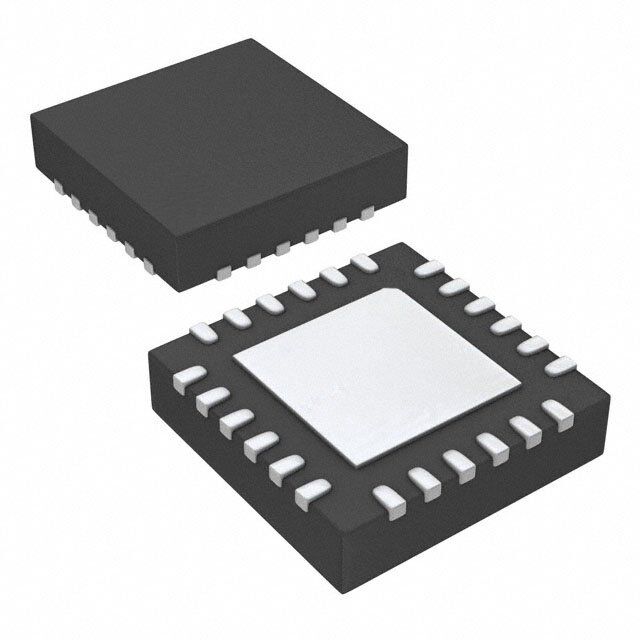
| 描述 | IC MIXER 500MHZ-2.7GHZ 24QFN |
| 产品分类 | RF 混频器 |
| 品牌 | Hittite Microwave Corporation |
| 数据手册 | 点击此处下载产品Datasheet |
| 产品图片 |  |
| 产品型号 | HMC915LP4E |
| RF类型 | 通用 |
| rohs | 无铅 / 符合限制有害物质指令(RoHS)规范要求 |
| 产品系列 | - |
| 供应商器件封装 | 24-QFN(4x4) |
| 其它名称 | 1127-1076-6 |
| 包装 | Digi-Reel® |
| 噪声系数 | 8.5dB |
| 增益 | - |
| 封装/外壳 | 24-VQFN 裸露焊盘 |
| 标准包装 | 1 |
| 混频器数 | 1 |
| 电压-电源 | 5V |
| 电流-电源 | 88mA |
| 辅助属性 | - |
| 配用 | /product-detail/zh/127416-HMC915LP4E/1127-1139-ND/3588442/product-detail/zh/115820-HMC915LP4E/115820-HMC915LP4E-ND/4692824 |
| 频率 | 500MHz ~ 2.7GHz |
Datasheet
PDF Datasheet 数据手册内容提取
HMC915LP4E v00.1009 GaAs MMIC MIXER w/ INTEGRATED LO AMPLIFIER, 0.5 - 2.7 GHz Typical Applications Features The HMC915LP4E is ideal for: Input IP3: +28 dBm • PCS / 3G Infrastructure Low Input LO Drive: -2 to +4 dBm • Base Stations & Repeaters High LO to RF Isolation: 28 dB • WiMAX & WiBro Low Conversion Loss: 8 dB 9 • ISM & Fixed Wireless Single Positive Supply: +5V @ 88 mA 24 Lead 4x4mm SMT Package: 16mm2 T M Functional Diagram General Description S The HMC915LP4E is a high linearity, double-balanced - converter that operates from 0.5 to 2.7 GHz and D delivers a +28 dBm input IP3. The LO amplifi er output E and high dynamic range mixer input are positioned C so that an external LO fi lter can be placed in series N between them if necessary. The converter provides A 28 dB of LO to RF isolation and is ideal for upconver- L ter and downconverter applications. The IC operates A from a single +5V supply consuming 88 mA and ac- B cepts LO drive levels of -2 to +4 dBm. The design E requires no external baluns and supports IF frequ- L encies between DC and 1 GHz. The HMC915LP4E is B pin for pin compatible with the HMC552LP4E and the U HMC215LP4E mixers with integrated LO amplifi ers. O D & E L Electrical Specifi cations, T = +25°C, LO = +2 dBm, Vcc = +5V, IF = 100 MHz* A G Parameter Min. Typ. Max. Min. Typ. Max. Units N Frequency Range, RF, LO 0.5 - 2.0 2.0 - 2.7 GHz I S Frequency Range, IF DC - 1.0 DC - 1.0 GHz - Conversion Loss 8 11 10 13 dB S Noise Figure (SSB) 8.5 10.5 dB R LO to RF Isolation 22 30 25 28 dB E LO to IF Isolation 10 16 12 18 dB X IP3 (Input) 28 28 dBm I M 1 dB Compression (Input) 18 20 dBm LO Drive Input Level (Typical) -2 to 4 +2 to 6 dBm Supply Current (Icc) 78 88 110 78 88 110 mA *Unless otherwise noted, all measurements performed as a downconverter, with low side LO and confi gured as shown in application circuit. For price, delivery, and to place orders, please contact Hittite Microwave Corporation: 9 - 398 20 Alpha Road, Chelmsford, MA 01824 Phone: 978-250-3343 Fax: 978-250-3373 Order On-line at www.hittite.com
HMC915LP4E v00.1009 GaAs MMIC MIXER w/ INTEGRATED LO AMPLIFIER, 0.5 - 2.7 GHz Conversion Gain vs. Conversion Gain vs. Temperature, IF = 100 MHz Temperature, IF = 1 GHz 0 0 -5 -5 B) B) d d N ( -10 N ( -10 AI AI G G ON -15 ON -15 SI SI 9 R R VE -20 ++2855CC VE -20 ++2855CC N -40C N -40C O O C C -25 -25 -30 -30 T 0.3 0.6 0.9 1.2 1.5 1.8 2.1 2.4 2.7 3 1.5 1.8 2.1 2.4 2.7 3 M FREQUENCY (GHz) FREQUENCY (GHz) S - D Isolation Conversion Gain vs. LO Drive E C 0 0 N -10 B) -5 A d B) N ( -10 L SOLATION (d --3200 VERSION GAI --2105 LO= -4 dBm E BA I N LO= -2 dBm L -40 LLROOF tttooo RIIFFF CO -25 LLLOOO=== 0++ 24d BddmBBmm B LO= +6 dBm U -50 -30 O 0.3 0.6 0.9 1.2 1.5 1.8 2.1 2.4 2.7 3 0.3 0.6 0.9 1.2 1.5 1.8 2.1 2.4 2.7 3 D FREQUENCY (GHz) FREQUENCY (GHz) & Upconverter Performance E Return Loss Input IP3 vs. LO Drive L G 0 40 N 35 I -5 S 30 B) OSS (d -10 Bm) 25 S - N L 3 (d 20 R ETUR -15 IP 15 LO= -4 dBm E R -20 LROF 105 LLLLOOOO==== ++ - 0224 ddddBBBBmmmm MIX LO= +6 dBm -25 0 0 1 2 3 4 5 6 0.3 0.6 0.9 1.2 1.5 1.8 2.1 2.4 2.7 3 FREQUENCY (GHz) FREQUENCY (GHz) For price, delivery, and to place orders, please contact Hittite Microwave Corporation: 20 Alpha Road, Chelmsford, MA 01824 Phone: 978-250-3343 Fax: 978-250-3373 9 - 399 Order On-line at www.hittite.com
HMC915LP4E v00.1009 GaAs MMIC MIXER w/ INTEGRATED LO AMPLIFIER, 0.5 - 2.7 GHz Upconverter Performance Conversion Gain vs. LO Drive IF Bandwidth 0 0 -5 -5 B) N (d -10 B) -10 ON GAI -15 NSE (d -15 9 ONVERSI -20 LLLOOO=== 0--42 d ddBBBmmm RESPO --2250 Conversion Gain, 0.8 GHz =LO < RF C LO= +2 dBm Conversion Gain, 2.25 GHz = LO > RF -25 LLOO== ++46 ddBBmm -30 Return Loss T -30 -35 M 0.3 0.6 0.9 1.2 1.5 1.8 2.1 2.4 2.7 3 0 0.2 0.4 0.6 0.8 1 1.2 1.4 1.6 1.8 FREQUENCY (GHz) FREQUENCY (GHz) S - D E Input IP3 vs. Temperature, IF = 100 MHz Input IP3 vs. Temperature, IF = 1 GHz C 50 50 N A 40 40 L A m) 30 m) 30 B dB dB E IP3 ( 20 IP3 ( 20 L +25C +25C B 10 +85C 10 +85C -40C -40C U O 0 0 0.3 0.6 0.9 1.2 1.5 1.8 2.1 2.4 2.7 3 1.5 1.8 2 2.2 2.5 2.7 3 D FREQUENCY (GHz) FREQUENCY (GHz) & E L Input IP3 vs. LO Drive, IF = 100 MHz Input IP2 vs. Temperature G 40 100 N SI 35 90 +25C 30 +85C 80 -40C - 25 S Bm) Bm) 70 R P3 (d 20 P2 (d 60 E I 15 I LO= -4 dBm X 10 LLOO== -02 d dBBmm 50 LO= +2 dBm MI 5 LLOO== ++46 ddBBmm 40 0 30 0.3 0.6 0.9 1.2 1.5 1.8 2.1 2.4 2.7 3 1.5 1.8 2 2.2 2.5 2.7 3 FREQUENCY (GHz) FREQUENCY (GHz) For price, delivery, and to place orders, please contact Hittite Microwave Corporation: 9 - 400 20 Alpha Road, Chelmsford, MA 01824 Phone: 978-250-3343 Fax: 978-250-3373 Order On-line at www.hittite.com
HMC915LP4E v00.1009 GaAs MMIC MIXER w/ INTEGRATED LO AMPLIFIER, 0.5 - 2.7 GHz Input IP2 vs. LO Drive Input P1dB vs. Temperature 90 24 80 22 70 m) 20 B P2 (dBm) 5600 T P1dB (d 1168 9 I U 40 P LO= -4 dBm N 14 LO= -2 dBm I +25C 30 LO= 0 dBm +85C LO= +2 dBm 12 -40C LO= +4 dBm 20 LO= +6 dBm 10 T 0.3 0.6 0.9 1.2 1.5 1.8 2.1 2.4 2.7 3 0.3 0.6 0.9 1.2 1.5 1.8 2.1 2.4 2.7 M FREQUENCY (GHz) FREQUENCY (GHz) S - D Absolute Maximum Ratings MxN Spurious @ IF Port E C Bias Voltage (Vdd) 5.5 Vdc nLO N RF Power Input +23 dBm mRF 0 1 2 3 A +10 dBm up to 1 GHz 0 xx -3.17 -23.34 -30.34 LO Power Input (Vcc = 5 Vdc) L +8 dBm from 1 - 4 GHz 1 -4.67 0.00 -23.67 -52.17 A Channel Temperature 150°C 2 -76.00 -71.34 -79.84 -71.84 B Continuous Pdiss (T = 85°C) 3 xx xx xx -74.67 0.546 W (derate 8.4 mW/°C above 85°C) 4 xx xx xx xx E Thermal Resistance RF Freq. = 1.9 GHz @ -5 dBm L 119 °C/W (junction to ground paddle) LO Freq. = 1.8 GHz @ 0 dBm B Storage Temperature -65 to +150°C All values in dBc below the IF output power level. U Operating Temperature -55 to +85°C O ESD Sensitivity (HBM) Class 1C D & E Typical Supply Current Harmonics of LO L G Vcc Icc (mA) nLO Spur @ RF Port N 4.5 67 mA LO Freq. (GHz) 1 2 3 4 I 5.0 88 mA 1.0 32 40 27 40 S 5.5 117 mA 1.4 28 19 25 30 - 1.8 29 16 30 42 S 2.2 33 18 27 44 R ELECTROSTATIC SENSITIVE DEVICE 2.6 35 23 34 41 E OBSERVE HANDLING PRECAUTIONS 3.0 34 20 41 44 X LO = 4 dBm I M All values in dBc below input LO level measured at RF port. For price, delivery, and to place orders, please contact Hittite Microwave Corporation: 20 Alpha Road, Chelmsford, MA 01824 Phone: 978-250-3343 Fax: 978-250-3373 9 - 401 Order On-line at www.hittite.com
HMC915LP4E v00.1009 GaAs MMIC MIXER w/ INTEGRATED LO AMPLIFIER, 0.5 - 2.7 GHz Outline Drawing 9 T M S - D E NOTES: C 1. LEADFRAME MATERIAL: COPPER ALLOY 2. DIMENSIONS ARE IN INCHES [MILLIMETERS] N 3. LEAD SPACING TOLERANCE IS NON-CUMULATIVE. A 4. PAD BURR LENGTH SHALL BE 0.15mm MAXIMUM. L PAD BURR HEIGHT SHALL BE 0.05mm MAXIMUM. A 5. PACKAGE WARP SHALL NOT EXCEED 0.05mm. 6. ALL GROUND LEADS AND GROUND PADDLE MUST BE SOLDERED TO PCB RF GROUND. B 7. REFER TO HITTITE APPLICATION NOTE FOR SUGGESTED LAND PATTERN. E L B U Package Information O Part Number Package Body Material Lead Finish MSL Rating Package Marking [1] D HMC915LP4E RoHS-compliant Low Stress Injection Molded Plastic 100% matte Sn MSL1 [2] H915 & XXXX [1] 4-Digit lot number XXXX E [2] Max peak refl ow temperature of 260 °C L G N I S - S R E X I M For price, delivery, and to place orders, please contact Hittite Microwave Corporation: 9 - 402 20 Alpha Road, Chelmsford, MA 01824 Phone: 978-250-3343 Fax: 978-250-3373 Order On-line at www.hittite.com
HMC915LP4E v00.1009 GaAs MMIC MIXER w/ INTEGRATED LO AMPLIFIER, 0.5 - 2.7 GHz Pin Descriptions Pin Number Function Description Interface Schematic 1 MIX LO This pin is DC coupled and matched to 50 Ohms. The pins are not connected internally; however, all data shown 2, 6 - 9, 9 N/C herein was measured with these pins connected to RF/DC 11 - 17, 19 - 24 ground externally. Power supply and output for the LO amplifi er. Three T 3 BIAS external bypass capacitors are recommended for optimum M performance, as illustrated in the application circuit. S - D Backside of package has exposed metal ground 4 GND paddle that must also be connected to ground. E C N This pin is DC coupled and matched to 50 Ohms. A 5 LO An off chip DC blocking capacitor is required. L A B This pin is DC coupled. For applications not requiring operation E to DC, this port should be DC blocked externally using a series capacitor whose value has been chosen to pass the necessary L 10 IF IF frequency range. For operation to DC, this pin must not B source/sink more than 18 mA of current or die non-function and U possible die failure will result. O D 18 RF This pin is DC coupled and matched to 50 Ohms. & E L G N I S - S R E X I M For price, delivery, and to place orders, please contact Hittite Microwave Corporation: 20 Alpha Road, Chelmsford, MA 01824 Phone: 978-250-3343 Fax: 978-250-3373 9 - 403 Order On-line at www.hittite.com
HMC915LP4E v00.1009 GaAs MMIC MIXER w/ INTEGRATED LO AMPLIFIER, 0.5 - 2.7 GHz Application Circuit 9 T M S Recommended Components Values - C3 1000 pF D C4 2.2 μF E C C1, C2, C5 100 pF N L1 24 nH A R1 1.8 Ohm L A B E L B U O D & E L G N I S - S R E X I M For price, delivery, and to place orders, please contact Hittite Microwave Corporation: 9 - 404 20 Alpha Road, Chelmsford, MA 01824 Phone: 978-250-3343 Fax: 978-250-3373 Order On-line at www.hittite.com
HMC915LP4E v00.1009 GaAs MMIC MIXER w/ INTEGRATED LO AMPLIFIER, 0.5 - 2.7 GHz Evaluation PCB 9 T M S - D E C N A L A B E L B U O D List of Materials for Evaluation PCB 115820 [1] & The circuit board used should use RF circuit des- Item Description ign techniques. Signal lines should have 50 ohm E J1 - J3 PCB Mount SMA RF Connector impedance while the package ground leads and L J4, J5 DC Pin G exposed paddle should be connected directly to C1, C2, C5 100 pF Chip Capacitor, 0402 Pkg. N the ground plane similar to that shown. A sufficient C3 1000 pF Chip Capacitor, 0603 Pkg. I number of via holes should be used to connect S C4 2.2 μF Capacitor, Tantalum the top and bottom ground planes. The evaluation L1 24 nH Chip Inductor, 0603 Pkg. - circuit board shown is available from Hittite upon S R1 1.8 Ohm Resistor, 1206 ¼ Watt Pkg. request. R U1 HMC915LP4E E PCB [2] 113417 Evaluation PCB X [1] Reference this number when ordering complete evaluation PCB I M [2] Circuit Board Material: Rogers 4350 or Arlon 25FR For price, delivery, and to place orders, please contact Hittite Microwave Corporation: 20 Alpha Road, Chelmsford, MA 01824 Phone: 978-250-3343 Fax: 978-250-3373 9 - 405 Order On-line at www.hittite.com