首页 > HMC717LP3E > 详情
 Datasheet下载
- 型号: HMC717LP3E
- 制造商: Hittite
- 库位|库存: xxxx|xxxx
- 要求:
| 数量阶梯 | 香港交货 | 国内含税 |
| +xxxx | $xxxx | ¥xxxx |
查看当月历史价格
查看今年历史价格
产品参数
| 参数 | 数值 |
| 产品目录 | 射频/IF 和 RFID |
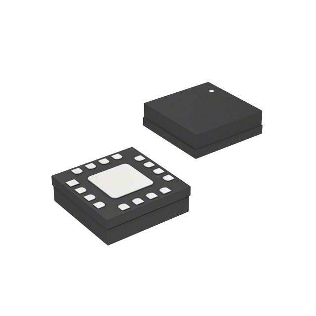
| 描述 | RF AMP LOW NOISE 6GHZ 16QFN |
| 产品分类 | RF 放大器 |
| 品牌 | Hittite Microwave Corporation |
| 数据手册 | 点击此处下载产品Datasheet |
| 产品图片 |  |
| P1dB | 18.5dBm |
| 产品型号 | HMC717LP3E |
| RF类型 | 通用 |
| rohs | 无铅 / 符合限制有害物质指令(RoHS)规范要求 |
| 产品系列 | - |
| 供应商器件封装 | 16-QFN(3x3) |
| 其它名称 | 1127-1189-1 |
| 包装 | 剪切带 (CT) |
| 噪声系数 | 1.1dB |
| 增益 | 16.5dB |
| 封装/外壳 | 16-VFQFN 裸露焊盘 |
| 标准包装 | 1 |
| 测试频率 | 4.8GHz ~ 6GHz |
| 电压-电源 | 3 V ~ 5 V |
| 电流-电源 | 73mA |
| 频率 | 4.8GHz ~ 6GHz |
Datasheet
PDF Datasheet 数据手册内容提取
HMC717LP3E v06.1113 GAAS PHEMT MMIC LOW NOISE AMPLIFIER, 4.8 - 6.0 GHz Typical Applications Features The HMC717LP3E is ideal for: Noise Figure: 1.1 dB E T •Fixed Wireless and LTE/WiMAX/4G Gain: 16.5 dB M •BTS & Infrastructure Output IP3: +31.5 dBm S •Repeaters and Femtocells Single Supply: +3V to +5V - T E •Public Safety Radio 16 Lead 3x3mm QFN Package: 9 mm2 S •Access Points I O E N Functional Diagram General Description W The HMC717LP3E is a GaAs PHEMT MMIC O L Low Noise Amplifi er that is ideal for fi xed wireless L and LTE/WiMAX/4G basestation front-end receivers - operating between 4.8 and 6.0 GHz. The amplifi er R O has been optimized to provide 1.1 dB noise fi gure, E 16.5 dB gain and +31.5 dBm output IP3 from a single I F supply of +5V. Input and output return losses are I excellent and the LNA requires minimal external L P matching and bias decoupling components. The S M HMC717LP3E can be biased with +3V to +5V and features an externally adjustable supply current A which allows the designer to tailor the linearity performance of the LNA for each application. B O Electrical Specifi cations T = +25° C, Rbias = 2k Ohms for Vdd = 5V, Rbias = 20k Ohms for Vdd = 3V [1] [2] A Vdd = +3V Vdd = +5V Parameter Units Min. Typ. Max. Min. Typ. Max. Frequency Range 4.8 - 6.0 4.8 - 6.0 GHz Gain 12 14.3 21 13.5 16.5 21 dB Gain Variation Over Temperature 0.01 0.01 dB/ °C Noise Figure 1.25 1.5 1.1 1.4 dB Input Return Loss 13 13 dB Output Return Loss 13 18 dB Output Power for 1 dB Compression (P1dB) 12 14 15 18.5 dBm Saturated Output Power (Psat) 15 19.5 dBm Output Third Order Intercept (IP3) 25.5 27 [3] 31.5 dBm Total Supply Current (Idd) 31 40 73 100 mA [1] Rbias resistor sets current, see application circuit herein [2] Vdd = Vdd1 = Vdd2 [3] Guaranteed by Design at 5GHz. For price, delivery and to place orders: Hittite Microwave Corporation, 2 Elizabeth Drive, Chelmsford, MA 01824 1 Phone: 978-250-3343 Fax: 978-250-3373 Order On-line at www.hittite.com Application Support: Phone: 978-250-3343 or apps@hittite.com
HMC717LP3E v06.1113 GAAS PHEMT MMIC LOW NOISE AMPLIFIER, 4.8 - 6.0 GHz Broadband Gain & Return Loss [1][2] Gain vs. Temperature [1] 25 25 20 E 15 S21 21 T 10 M B) d 5 RESPONSE (-1-050 S11 GAIN (dB) 1137 T E - S -15 S -20 9 S22 I -25 O E -30 5 1 2 3 4 5 6 7 8 9 10 4.5 4.9 5.3 5.7 6.1 6.5 N FREQUENCY (GHz) FREQUENCY (GHz) W Vdd=5V Vdd=3V +25C +85C -40C L O L Gain vs. Temperature [2] Input Return Loss vs. Temperature [1] - R 25 O 0 E 21 B) -5 FI d I GAIN (dB) 1137 S URN LOSS (-10 MPL T RE-15 A 9 B 5 -20 4.5 4.9 5.3 5.7 6.1 6.5 4.5 4.9 5.3 5.7 6.1 6.5 FREQUENCY (GHz) FREQUENCY (GHz) +25C +85C -40C +25C +85C -40C O Output Return Loss vs. Temperature [1] Reverse Isolation vs. Temperature [1] 0 -20 -25 -5 B) URN LOSS (d--1150 OLATION (dB)--3350 RET IS-40 -20 -45 -25 -50 4.5 4.9 5.3 5.7 6.1 6.5 4.5 4.9 5.3 5.7 6.1 6.5 FREQUENCY (GHz) FREQUENCY (GHz) +25C +85C -40C +25C +85C -40C [1] Vdd = 5V, Rbias = 2kΩ [2] Vdd = 3V, Rbias = 20kΩ For price, delivery and to place orders: Hittite Microwave Corporation, 2 Elizabeth Drive, Chelmsford, MA 01824 Phone: 978-250-3343 Fax: 978-250-3373 Order On-line at www.hittite.com 2 Application Support: Phone: 978-250-3343 or apps@hittite.com
HMC717LP3E v06.1113 GAAS PHEMT MMIC LOW NOISE AMPLIFIER, 4.8 - 6.0 GHz Noise Figure vs. Temperature [1] [2] [4] P1dB vs. Temperature [1] [2] 2.1 24 +85C T 1.8 22 Vdd=5V E M B) 1.5 20 d E - S OISE FIGURE ( 01..92 P1dB (dBm) 111468 T S N 0.6 +25C -40C 12 I 0.3 10 O EVdd=3V 0 8 N 4.5 4.9 5.3 5.7 6.1 6.5 4.5 4.9 5.3 5.7 6.1 6.5 FREQUENCY (GHz) FREQUENCY (GHz) W Vdd=5V Vdd=3V +25C +85C -40C O L L - Psat vs. Temperature [1] [2] Output IP3 vs. Temperature [1] [2] R 24 O 40 E 22 Vdd=5V 37 Vdd=5V I F 20 34 I L m) 18 m) 31 MP Psat (dB 1146 S IP3 (dB 2258 A 12 22 10 Vdd=3V 19 B Vdd=3V 8 16 4.5 4.9 5.3 5.7 6.1 6.5 4.5 4.9 5.3 5.7 6.1 6.5 FREQUENCY (GHz) FREQUENCY (GHz) +25C +85C -40C +25C +85C -40C O Output IP3 and Total Supply Current vs. Output IP3 and Total Supply Current vs. Supply Voltage @ 4800 MHz [3] Supply Voltage @ 5900 MHz [3] 32 110 34 125 30 95 32 110 30 95 28 80 3 (dBm) 26 65 Idd (m 3 (dBm) 2268 6850 Idd (m P A P A I 24 50 ) I ) 24 50 22 35 22 35 20 20 20 20 2.7 3.1 3.5 3.9 4.3 4.7 5.1 5.5 2.7 3.1 3.5 3.9 4.3 4.7 5.1 5.5 Voltage Supply (V) Voltage Supply (V) IP3-3V Idd-3V IP3-3V Idd-3V IP3-5V Idd-5V IP3-5V Idd-5V [1] Vdd = 5V, Rbias = 2k Ω [2] Vdd = 3V, Rbias = 20kΩ [3] Rbias = 2kΩ for Vdd = 5V, Rbias = 20kΩ for Vdd = 3V [4] Measurement reference plane shown on evaluation PCB drawing. For price, delivery and to place orders: Hittite Microwave Corporation, 2 Elizabeth Drive, Chelmsford, MA 01824 3 Phone: 978-250-3343 Fax: 978-250-3373 Order On-line at www.hittite.com Application Support: Phone: 978-250-3343 or apps@hittite.com
HMC717LP3E v06.1113 GAAS PHEMT MMIC LOW NOISE AMPLIFIER, 4.8 - 6.0 GHz Power Compression @ 4800 MHz [1] Power Compression @ 4800 MHz [2] 25 25 %)20 %) 20 E T PAE (15 PAE ( 15 M N (dB), 10 N (dB), 10 S GAI 5 GAI 5 T - m), m), E Pout (dB -50 Pout (dB -05 IS O E -10 -10 -20 -15 -10 -5 0 5 -20 -17 -14 -11 -8 -5 -2 1 4 N INPUT POWER (dBm) INPUT POWER (dBm) W Pout Gain PAE Pout Gain PAE L O L Power Compression @ 5900 MHz [1] Power Compression @ 5900 MHz [2] - R 25 O 25 E E (%) 20 E (%) 20 FI B), PA 15 B), PA 15 LI AIN (d 10 S AIN (d 10 P G 5 G 5 M m), m), dB 0 dB 0 A ut ( ut ( Po -5 Po -5 B -10 -10 -20 -16 -12 -8 -4 0 4 8 -20 -15 -10 -5 0 5 INPUT POWER (dBm) INPUT POWER (dBm) Pout Gain PAE Pout Gain PAE O Gain, Power & Noise Figure Gain, Power & Noise Figure vs. Supply Voltage @ 4800 MHz [3] vs. Supply Voltage @ 5900 MHz [3] 22 1.6 22 1.6 20 1.5 20 1.5 B) & P1dB (dBm) 111468 111...234 NOISE FIGUR B) & P1dB (dBm) 1168 11..34 NOISE FIGUR ain (d 12 1.1 E (dB ain (d 14 1.2 E (dB G ) G ) 10 1 12 1.1 8 0.9 10 1 2.7 3.1 3.5 3.9 4.3 4.7 5.1 5.5 2.7 3.1 3.5 3.9 4.3 4.7 5.1 5.5 Voltage Supply (V) Voltage Supply (V) GP1adinB NF GP1adinB NF [1] Vdd = 5V, Rbias = 2k Ω [2] Vdd = 3V, Rbias = 20kΩ [3] Rbias = 2kΩ for Vdd = 5V, Rbias = 20kΩ for Vdd = 3V For price, delivery and to place orders: Hittite Microwave Corporation, 2 Elizabeth Drive, Chelmsford, MA 01824 Phone: 978-250-3343 Fax: 978-250-3373 Order On-line at www.hittite.com 4 Application Support: Phone: 978-250-3343 or apps@hittite.com
HMC717LP3E v06.1113 GAAS PHEMT MMIC LOW NOISE AMPLIFIER, 4.8 - 6.0 GHz Output IP3 vs. Rbias @ 4800 MHz Gain, Noise Figure & Rbias @ 4800 MHz 32 20 2.2 E T 30 17 2 M 28 14 1.8 NO - S IP3 (dBm) 26 GAIN (dB) 11 T 1.6 ISE FIGUR E 24 8 1.4 E (d S B) 22 5 1.2 I O E 20 2 1 N 100 1000 10000 100000 100 1000 10000 100000 Rbias (Ohms) Rbias (Ohms) W Vdd=3V Vdd=5V Vdd=3V Vdd=5V O L L - Output IP3 vs. Rbias @ 5900 MHz Gain, Noise Figure & Rbias @ 5900 MHz R 35 O 18 1.7 E FI 32 16 1.6 LI 14 1.5 NO MP IP3 (dBm) 2269 S GAIN (dB) 12 1.4 ISE FIGUR A 10 1.3 E (d B 23 ) 8 1.2 B 20 6 1.1 100 1000 10000 100000 100 1000 10000 100000 Rbias (Ohms) Rbias (Ohms) Vdd=3V Vdd=5V Vdd=3V Vdd=5V O For price, delivery and to place orders: Hittite Microwave Corporation, 2 Elizabeth Drive, Chelmsford, MA 01824 5 Phone: 978-250-3343 Fax: 978-250-3373 Order On-line at www.hittite.com Application Support: Phone: 978-250-3343 or apps@hittite.com
HMC717LP3E v06.1113 GAAS PHEMT MMIC LOW NOISE AMPLIFIER, 4.8 - 6.0 GHz Absolute Bias Resistor Range & Recommended Bias Resistor Values Rbias (Ohms) Vdd (V) Idd (mA) E Min Max Recommended T 2k 20 M 3V 2k [1] Open Circuit 4.7k 26 S 20k 31 T - 261 50 E 5V 150 [2] Open Circuit 1k 65 S 2k 73 I O E [1] With Vdd= 3V and Rbias < 2kΩ may result in the part becoming conditionally stable which is not recommended. N [2] With Vdd = 5V and Rbias<150Ω may result in the part becoming conditionally stable which is not recommended. W L O L - Absolute Maximum Ratings R O Drain Bias Voltage (Vdd) +5.5V E ELECTROSTATIC SENSITIVE DEVICE I RF Input Power (RFIN) F +20 dBm (Vdd = +5 Vdc) OBSERVE HANDLING PRECAUTIONS I L Channel Temperature 150 °C P S Continuous Pdiss (T= 85 °C) 0.5 W M (derate 7.73 mW/°C above 85 °C) A Thermal Resistance 129.5 °C/W (channel to ground paddle) Storage Temperature B -65 to +150 °C Operating Temperature -40 to +85 °C ESD Sensitivity (HBM) Class 1A O Typical Supply Current vs. Supply Voltage (Rbias = 2kΩ for Vdd = 5V, Rbias = 20kΩ for Vdd = 3V) Vdd (V) Idd (mA) 2.7 23 3.0 31 3.3 39 4.5 60 5.0 73 5.5 85 Note: Amplifi er will operate over full voltage ranges shown above. For price, delivery and to place orders: Hittite Microwave Corporation, 2 Elizabeth Drive, Chelmsford, MA 01824 Phone: 978-250-3343 Fax: 978-250-3373 Order On-line at www.hittite.com 6 Application Support: Phone: 978-250-3343 or apps@hittite.com
HMC717LP3E v06.1113 GAAS PHEMT MMIC LOW NOISE AMPLIFIER, 4.8 - 6.0 GHz Outline Drawing E T M S - T E S I O E N W O L L - R O E I F I L NOTES: P 1. LEADFRAME MATERIAL: COPPER ALLOY S M 2. DIMENSIONS ARE IN INCHES [MILLIMETERS] 3. LEAD SPACING TOLERANCE IS NON-CUMULATIVE A 4. PAD BURR LENGTH SHALL BE 0.15mm MAXIMUM. PAD BURR HEIGHT SHALL BE 0.05mm MAXIMUM. 5. PACKAGE WARP SHALL NOT EXCEED 0.05mm. B 6. ALL GROUND LEADS AND GROUND PADDLE MUST BE SOLDERED TO PCB RF GROUND. 7. REFER TO HITTITE APPLICATION NOTE FOR SUGGESTED LAND PATTERN. O Package Information Part Number Package Body Material Lead Finish MSL Rating Package Marking [3] HMC717LP3E RoHS-compliant Low Stress Injection Molded Plastic 100% matte Sn MSL1 [2] 717 XXXX [1] Max peak refl ow temperature of 235 °C [2] Max peak refl ow temperature of 260 °C [3] 4-Digit lot number XXXX For price, delivery and to place orders: Hittite Microwave Corporation, 2 Elizabeth Drive, Chelmsford, MA 01824 7 Phone: 978-250-3343 Fax: 978-250-3373 Order On-line at www.hittite.com Application Support: Phone: 978-250-3343 or apps@hittite.com
HMC717LP3E v06.1113 GAAS PHEMT MMIC LOW NOISE AMPLIFIER, 4.8 - 6.0 GHz Pin Descriptions Pin Number Function Description Interface Schematic E 1, 3 - 7, 9, 10, No connection required. These pins may be connected T N/C 12, 14, 16 to RF/DC ground without affecting performance. M S This pin is DC coupled T - 2 RFIN See the application circuit for off-chip component. E S I O E This pin is used to set the DC current of the amplifi er by N 8 BIAS selection of the external bias resistor. See application circuit. W L O L 11 RFOUT This pin is AC coupled and matched to 50 Ohms - R O E I F I L Power supply voltage. Bypass capacitors are required. 13, 15 Vdd2, Vdd1 S See application circuit. P M A B GND Package bottom must be connected to RF/DC ground O For price, delivery and to place orders: Hittite Microwave Corporation, 2 Elizabeth Drive, Chelmsford, MA 01824 Phone: 978-250-3343 Fax: 978-250-3373 Order On-line at www.hittite.com 8 Application Support: Phone: 978-250-3343 or apps@hittite.com
HMC717LP3E v06.1113 GAAS PHEMT MMIC LOW NOISE AMPLIFIER, 4.8 - 6.0 GHz Application Circuit E T M S - T E S I O E N W O L L - R O E I F I L P S M A B O For price, delivery and to place orders: Hittite Microwave Corporation, 2 Elizabeth Drive, Chelmsford, MA 01824 9 Phone: 978-250-3343 Fax: 978-250-3373 Order On-line at www.hittite.com Application Support: Phone: 978-250-3343 or apps@hittite.com
HMC717LP3E v06.1113 GAAS PHEMT MMIC LOW NOISE AMPLIFIER, 4.8 - 6.0 GHz Evaluation PCB E T M S T - E S I O E N W L O L - R O E I F I L P S M A B O List of Materials for Evaluation PCB 122416 [1] The circuit board used in this application should use Item Description RF circuit design techniques. Signal lines should J1, J2 PCB Mount SMA Connector have 50 Ohm impedance while the package ground J3 - J5 DC Pins leads and exposed paddle should be connected C1 10 nF Capacitor, 0402 Pkg. directly to the ground plane similar to that shown. C2, C4 1000 pF Capacitor, 0603 Pkg. A sufficient number of via holes should be used to C3, C5 100 pF Capacitor, 0603 Pkg. connect the top and bottom ground planes. The C6 1.2 pF Capacitor, 0402 Pkg. evaluation board should be mounted to an appro- R1 2k Ohm Resistor, 0402 Pkg. (Rbias) priate heat sink. The evaluation circuit board shown R2, R3 0 Ohm Resistor, 0402 Pkg. is available from Hittite upon request. U1 HMC717LP3E Amplifi er PCB [2] 120586 Evaluation PCB [1] Reference this number when ordering complete evaluation PCB [2] Circuit Board Material: Rogers 4350. For price, delivery and to place orders: Hittite Microwave Corporation, 2 Elizabeth Drive, Chelmsford, MA 01824 Phone: 978-250-3343 Fax: 978-250-3373 Order On-line at www.hittite.com 10 Application Support: Phone: 978-250-3343 or apps@hittite.com