首页 > HMC655LP2E > 详情

 Datasheet下载
- 型号: HMC655LP2E
- 制造商: Hittite
- 库位|库存: xxxx|xxxx
- 要求:
| 数量阶梯 | 香港交货 | 国内含税 |
| +xxxx | $xxxx | ¥xxxx |
查看当月历史价格
查看今年历史价格
产品参数
| 参数 | 数值 |
| 产品目录 | 射频/IF 和 RFID |
| 描述 | IC ATTENUATOR PASSIVE 6-DFN |
| 产品分类 | 衰减器 |
| 品牌 | Hittite Microwave Corporation |
| 数据手册 | 点击此处下载产品Datasheet |
| 产品图片 | 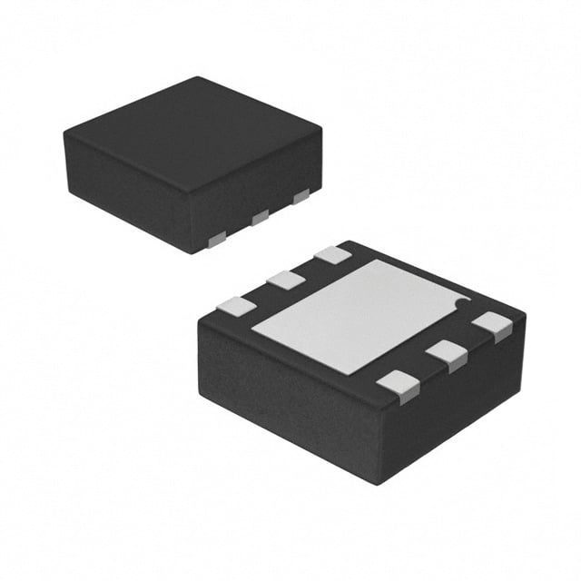 |
| 产品型号 | HMC655LP2E |
| rohs | 无铅 / 符合限制有害物质指令(RoHS)规范要求 |
| 产品系列 | - |
| 其它名称 | 1127-1510 1127-1510-1 1127-1510-ND |
| 功率(W) | - |
| 容差 | ±0.5dB |
| 封装/外壳 | 6-VDFN 裸露焊盘 |
| 标准包装 | 1 |
| 衰减值 | 6dB |
| 阻抗 | 50 欧姆 |
| 频率范围 | 0 ~ 25GHz |
Datasheet
PDF Datasheet 数据手册内容提取
HMC652LP2E HMC655LP2E to v02.0112 WIDEBAND FIXED ATTENUATOR FAMILY, DC - 25 GHz HMC652LP2E / HMC653LP2E / HMC654LP2E / HMC655LP2E Typical Applications Features The HMC652LP2E - HMC655LP2E are ideal for: 4 Attenuator Products: 2, 3, 4 & 6 dB Fixed Attenuation Levels • Fiber Optics Wide Bandwidth: DC - 25 GHz • Microwave Radio Excellent Attenuation Accuracy • Military & Space Power Handling: +25 dBm • Test & Measurement 6 Lead 2x2 mm SMT Package: 4 mm2 • Scientific Instruments • RF / Microwave Circuit Prototyping 12 Functional Diagram General Description T The HMC652LP2E / 653LP2E / 654LP2E / 655LP2E M are a line of wideband fixed value SMT 50 Ohm S matched attenuators which offer attenuation levels - of 2, 3, 4 and 6 dB respectively. These passive S attenuators are ideal for military, test equipment, and E other wideband applications where extremely flat V attenuation, and excellent VSWR vs. frequency are I S required. S A These wideband attenuators handle up to +25 dBm P of input power, and are compatible with high volume surface mount manufacturing techniques. Electrical Specifications, T = +25° C, 50 Ohm system A Return Loss Return Loss Attenuation Tolerance [1] Temperature Coefficient (Typicial) [2] Units Part Number Attenuator Value (Min.) (Typ.) DC - 25 GHz HMC652LP2E 2 dB 7.0 22.0 ± 0.5 0.0004 dB HMC653LP2E 3 dB 7.0 23.0 ± 0.5 0.0006 dB HMC654LP2E 4 dB 7.0 20.5 ± 0.5 0.0006 dB HMC655LP2E 6 dB 7.0 16.5 ± 0.5 0.0004 dB [1] Attenuation Tolerance is valid over temperature. [2] Temperature Coefficient Units are dB/ °C. InfoFrmoatrio pn rfuicrneish,e dd ebyli vAenarloyg aDnevdic etso i sp blealiceveed o tor dbee rasc:c uHratiet taitned rMeliaicblreo. Hwoawevveer , Cnoo rpFoorra ptiroicne,, 2de0l ivAelrpy,h aan dR otoa pdla, cCe hoerdlmerss:f oArnda,lo Mg AD e0v1ic8e2s,4 Inc., responsibility is assumed by Analog Devices for its use, nor for any infringements of patents or other One Technology Way, P.O. Box 9106, Norwood, MA 02062-9106 12 - 1 rliicgehntss eo fi sth girrda nptaerdti ebsy t himatp mlicaPayt hiorenos uonlrt e ofr:toh me9r wi7tsi8s ue-s eu2.n 5dSep0re -ca3infiyc3 ap4tiaot3nesn t s ou rb jFpeacatte txnot : c rhi9gah7ntgs8 eo- wf2 Ait5hnoa0ulot- gn3 oD3tiec7vei.c3 eN so . OPhrodneer: 7O8n1--3l2in9e-4 a70t 0w (cid:127)w Owrd.ehr iottniltiene.c aot mwww.analog.com Trademarks and registered trademarks aAre pthpe plircopaerttiyo onf t hSeiru repsppeoctirvte: o Pwnheros.ne: 978-250-33A4p3pl i coarti o an pSpupsp@orht:i tPtihtoen.ec:o 1m-800-ANALOG-D
HMC652LP2E HMC655LP2E to v02.0112 WIDEBAND FIXED ATTENUATOR FAMILY, DC - 25 GHz HMC652LP2E / HMC653LP2E / HMC654LP2E / HMC655LP2E Attenuation vs. Temperature Return Loss 0 0 -1 HMC652LP2 -5 -2 B) -3 B) HMC653LP2E UATION (d --54 HHMMCC665534LLPP22 N LOSS (d--1150 HMC654LP2E N -6 R TTE -7 HMC655LP2 ETU-20 HMC655LP2E A R -8 +25C -25 +85C -9 -40C HMC652LP2E 12 -10 -30 0 5 10 15 20 25 0 5 10 15 20 25 FREQUENCY (GHz) FREQUENCY (GHz) T M S Absolute Maximum Ratings - S Part Number HMC652LP2E HMC653LP2E HMC654LP2E HMC655LP2E Units E RF Input Power (CW) 27 26 25 26 dBm V I DC Voltage Terminated 5.6 5.2 4.9 5.2 V S DC Voltage Open 5.6 5.1 4.6 6.0 V S A Storage Temperature -65 to +150 °C P Operating Temperature -40 to +85 °C ESD Sensitivity (HBM) Class 1A Class 1A Class 1A Class 1A ELECTROSTATIC SENSITIVE DEVICE OBSERVE HANDLING PRECAUTIONS InfoFrmoarti opn rfiucrneis,h edd eblyi vAenarlyog a Dnedvic etos isp blaelcieeve do trod beer asc:c uHraittet iatned Mreliiacbrleo. wHoawvevee r,C noo rpFoorra tpiroicne,, 2d0el iAvelrpyh, aan Rd otoa dpl,a cCeh oerldmerssf:o Arnda,l oMg AD e0v1ic8e2s4, Inc., responsibility is assumed by Analog Devices for its use, nor for any infringements of patents or other One Technology Way, P.O. Box 9106, Norwood, MA 02062-9106 rights of third parties that mPayh roesnulet f:ro m9 7its8 u-s2e.5 S0pe-c3ifi3ca4tio3n s s u bFjeact xto: c9ha7n8ge- 2wi5th0ou-t 3no3tic7e3. N o OPrhdoneer: O78n1--3li2n9e- 4a7t0 0w (cid:127)w Owrd.ehri totnitlein.ec aot mwww.analog.com 12 - 2 license is granted by implication or otherwise under any patent or patent rights of Analog Devices. Trademarks and registered trademarks aArep thpe lpircopaetrityo onf thSeiur rpesppeoctrivte: oPwhneorsn.e: 978-250-33A4p3p l icoart i oanp Spusp@pohrti:t Ptihteo.nceo: 1m-800-ANALOG-D
HMC652LP2E HMC655LP2E to v02.0112 WIDEBAND FIXED ATTENUATOR FAMILY, DC - 25 GHz HMC652LP2E / HMC653LP2E / HMC654LP2E / HMC655LP2E Outline Drawing 12 T M S NOTES: 1. LEADFRAME MATERIAL: COPPER ALLOY - 2. DIMENSIONS ARE IN INCHES [MILLIMETERS] S 3. LEAD SPACING TOLERANCE IS NON-CUMULATIVE. E 4. PAD BURR LENGTH SHALL BE 0.15mm MAXIMUM. V PAD BURR HEIGHT SHALL BE 0.05mm MAXIMUM. 5. PACKAGE WARP SHALL NOT EXCEED 0.05mm. I S 6. ALL GROUND LEADS AND GROUND PADDLE MUST BE S SOLDERED TO PCB RF GROUND. 7. REFER TO HITTITE APPLICATION NOTE FOR SUGGESTED A LAND PATTERN. P Package Information Part Number Package Body Material Lead Finish MSL Rating Package Marking [1] HMC652LP2E through RoHS-compliant Low Stress Injection 100% matte Sn MSL1 [2] NNN HMC655LP2E Molded Plastic XXX [1] 3-Digit lot number XXX [2] Max peak reflow temperature of 260 °C Pin Descriptions Pin Number Function Description Interface Schematic 1, 3, 4, 6 GND Package bottom must be connected to RF/DC ground. This pin is DC coupled and matched to 50 Ohms. 2, 5 RF1, RF2 Use DC Blocking capacitors if the input / output signals have non-zero DC potential InfoFrmoatrio pn rfuicrneish,e dd ebyli vAenarloyg aDnevdic etso i sp blealiceveed o tor dbee rasc:c uHratiet taitned rMeliaicblreo. Hwoawevveer , Cnoo rpFoorra ptiroicne,, 2de0l ivAelrpy,h aan dR otoa pdla, cCe hoerdlmerss:f oArnda,lo Mg AD e0v1ic8e2s,4 Inc., responsibility is assumed by Analog Devices for its use, nor for any infringements of patents or other One Technology Way, P.O. Box 9106, Norwood, MA 02062-9106 12 - 3 rliicgehntss eo fi sth girrda nptaerdti ebsy t himatp mlicaPayt hiorenos uonlrt e ofr:toh me9r wi7tsi8s ue-s eu2.n 5dSep0re -ca3infiyc3 ap4tiaot3nesn t s ou rb jFpeacatte txnot : c rhi9gah7ntgs8 eo- wf2 Ait5hnoa0ulot- gn3 oD3tiec7vei.c3 eN so . OPhrodneer: 7O8n1--3l2in9e-4 a70t 0w (cid:127)w Owrd.ehr iottniltiene.c aot mwww.analog.com Trademarks and registered trademarks aAre pthpe plircopaerttiyo onf t hSeiru repsppeoctirvte: o Pwnheros.ne: 978-250-33A4p3pl i coarti o an pSpupsp@orht:i tPtihtoen.ec:o 1m-800-ANALOG-D
HMC652LP2E HMC655LP2E to v02.0112 WIDEBAND FIXED ATTENUATOR FAMILY, DC - 25 GHz HMC652LP2E / HMC653LP2E / HMC654LP2E / HMC655LP2E Evaluation PCB 12 T M S - S E V I S S A P List of Materials for Evaluation PCB 119197 [1] The circuit board used in the final application should Item Description be generated with proper RF circuit design tech- J1 - J2 PCB Mount K Connector niques. Signal lines at the RF port should have 50 HMC652LP2E through HMC655LP2E U1 Passive Attenuators ohm impedance and the package ground leads and PCB [2] 119194 Evaluation PCB exposed paddle should be connected directly to [1] Reference this number when ordering complete evaluation PCB the ground plane similar to that shown above. The [2] Circuit Board Material: Rogers 4350 evaluation circuit board shown above is available from Hittite Microwave Corporation upon request. InfoFrmoarti opn rfiucrneis,h edd eblyi vAenarlyog a Dnedvic etos isp blaelcieeve do trod beer asc:c uHraittet iatned Mreliiacbrleo. wHoawvevee r,C noo rpFoorra tpiroicne,, 2d0el iAvelrpyh, aan Rd otoa dpl,a cCeh oerldmerssf:o Arnda,l oMg AD e0v1ic8e2s4, Inc., responsibility is assumed by Analog Devices for its use, nor for any infringements of patents or other One Technology Way, P.O. Box 9106, Norwood, MA 02062-9106 rights of third parties that mPayh roesnulet f:ro m9 7its8 u-s2e.5 S0pe-c3ifi3ca4tio3n s s u bFjeact xto: c9ha7n8ge- 2wi5th0ou-t 3no3tic7e3. N o OPrhdoneer: O78n1--3li2n9e- 4a7t0 0w (cid:127)w Owrd.ehri totnitlein.ec aot mwww.analog.com 12 - 4 license is granted by implication or otherwise under any patent or patent rights of Analog Devices. Trademarks and registered trademarks aArep thpe lpircopaetrityo onf thSeiur rpesppeoctrivte: oPwhneorsn.e: 978-250-33A4p3p l icoart i oanp Spusp@pohrti:t Ptihteo.nceo: 1m-800-ANALOG-D