首页 > HMC632LP5E > 详情
 Datasheet下载
- 型号: HMC632LP5E
- 制造商: Hittite
- 库位|库存: xxxx|xxxx
- 要求:
| 数量阶梯 | 香港交货 | 国内含税 |
| +xxxx | $xxxx | ¥xxxx |
查看当月历史价格
查看今年历史价格
产品参数
| 参数 | 数值 |
| 产品目录 | 射频/IF 和 RFID |
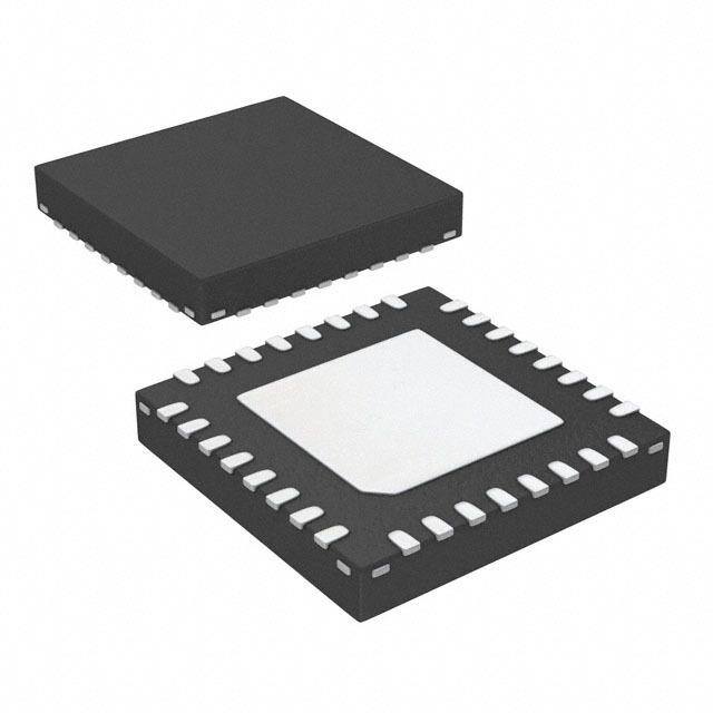
| 描述 | IC MMIC VCO HBT BIPOLAR 32-QFN |
| 产品分类 | RF 其它 IC 和模块 |
| 品牌 | Hittite Microwave Corporation |
| 数据手册 | 点击此处下载产品Datasheet |
| 产品图片 |  |
| 产品型号 | HMC632LP5E |
| RF类型 | 通用 |
| rohs | 无铅 / 符合限制有害物质指令(RoHS)规范要求 |
| 产品系列 | - |
| 供应商器件封装 | 32-SMT (5x5) |
| 其它名称 | 1127-1499 |
| 功能 | VCO |
| 包装 | 剪带 |
| 封装/外壳 | 32-VFQFN 裸露焊盘 |
| 标准包装 | 50 |
| 特色产品 | http://www.digikey.cn/product-highlights/zh/vcos/52289 |
| 辅助属性 | 三路输出(除以 2,除以 4,标准) |
| 频率 | 14.25GHz ~ 15.65GHz |
Datasheet
PDF Datasheet 数据手册内容提取
HMC632LP5 632LP5E / v03.0811 MMIC VCO w/ HALF FREQUENCY OUTPUT & DIVIDE-BY-4, 14.25 - 15.65 GHz Typical Applications Features The HMC632LP5(E) is ideal for: Dual Output: Fo = 14.25 - 15.65 GHz Fo/2 = 7.125 - 7.825 GHz • Point to Point/Multipoint Radio Pout: +9 dBm • Test Equipment & Industrial Controls Phase Noise: -107 dBc/Hz @100 kHz Typ. • SATCOM No External Resonator Needed • Military End-Use 32 Lead 5x5mm SMT Package: 25mm² Functional Diagram General Description The HMC632LP5(E) is a GaAs InGaP Heterojunc- tion Bipolar Transistor (HBT) MMIC VCO. The HMC632LP5(E) integrates resonators, negative resis- tance devices, varactor diodes and features half- frequency and divide-by-4 outputs. The VCO’s phase noise performance is excellent over temperature, shock, and process due to the oscillator’s monolithic 8 structure. Power output is +9 dBm typical from a +5V supply voltage. The prescaler and RF/2 functions can be disabled to conserve current if not required. The voltage controlled oscillator is packaged in a leadless T M QFN 5x5 mm surface mount package, and requires no external matching components. S - T U P T Electrical Specifications, T = +25° C, Vcc (Dig), Vcc (Amp), Vcc (RF) = +5V A U O Parameter Min. Typ. Max. Units Frequency Range Fo 14.25 - 15.65 GHz 2 Fo/2 7.125 - 7.825 GHz / o RFOUT 4 12 dBm F Power Output RFOUT/2 7 13 dBm RFOUT/4 -8 -2 dBm h SSB Phase Noise @ 100 kHz Offset, t -107 dBc/Hz Vtune= +5V @ RFOUT i w Tune Voltage Vtune 2 13 V S Supply Current Icc(Dig) + Icc(Amp) + Icc(RF) 280 350 400 mA O Tune Port Leakage Current (Vtune= 13V) 10 µA C Output Return Loss 2 dB V Harmonics/Subharmonics 1/2 25 dBc 2nd 25 dBc Pulling (into a 2.0:1 VSWR) 10 MHz pp Pushing @ Vtune= 5V 35 MHz/V Frequency Drift Rate 1.0 MHz/°C InfoFrmoarti opn rfiucrneis,h edd eblyi vAenarlyog a Dnedvic etos isp blaelcieeve do trod beer asc:c uHraittet iatned Mreliiacbrleo. wHoawvevee r,C noo rpFoorra tpiroicne,, 2d0el iAvelrpyh, aan Rd otoa dpl,a cCeh oerldmerssf:o Arnda,l oMg AD e0v1ic8e2s4, Inc., responsibility is assumed by Analog Devices for its use, nor for any infringements of patents or other One Technology Way, P.O. Box 9106, Norwood, MA 02062-9106 8 - 1 rliicgehntss eo fi sth girrda nptaerdti ebsy t himatp mlicPaayht ioroens nuolret of:rto hm9er 7wits8is ue-s 2eu.n5 dS0epre- ca3infi3yc ap4tiao3tne sn ts ou rb Fjpeaactte xtno:t cr9higa7hnt8gs e-o 2wf Ai5thn0oaulo-t g3n oD3tiec7vei3.c eN s o. OPrhdoneer: O78n1--3li2n9e- 4a7t0 0w (cid:127)w Owrd.ehri totnitlein.ec aot mwww.analog.com Trademarks and registered trademarks aArep thpe lpircopaetrityo onf thSeiur rpesppeoctrivte: oPwhneorsn.e: 978-250-33A4p3p l icoart i oanp Spusp@pohrti:t Ptihteo.nceo: 1m-800-ANALOG-D
HMC632LP5 / 632LP5E v03.0811 MMIC VCO w/ HALF FREQUENCY OUTPUT & DIVIDE-BY-4, 14.25 - 15.65 GHz Frequency vs. Tuning Voltage, Vcc = +5V Frequency vs. Tuning Voltage, T= 25°C 17 17 Hz) 16 Hz) 16 G G CY ( 15 CY ( 15 N N E E U U Q 14 Q 14 E E R R F F UT 13 ++2855CC UT 13 VVcccc == 45..7050VV TP -40C TP Vcc = 5.25V U U O 12 O 12 11 11 0 1 2 3 4 5 6 7 8 9 10 11 12 13 0 1 2 3 4 5 6 7 8 9 10 11 12 13 TUNING VOLTAGE (V) TUNING VOLTAGE (V) Output Power Sensitivity vs. Tuning Voltage, Vcc = +5V vs. Tuning Voltage, Vcc = +5V 900 16 800 14 8 V) 700 12 MHz/ 600 Bm) 10 NSITIVITY ( 345000000 ++-428055CCC POWER (d 68 +25C MT SE 200 4 +-4805CC S 100 2 - T 0 0 0 1 2 3 4 5 6 7 8 9 10 11 12 13 0 1 2 3 4 5 6 7 8 9 10 11 12 13 U TUNING VOLTAGE (V) TUNING VOLTAGE (V) P T U O SSB Phase Noise vs. Tuning Voltage SSB Phase Noise @ Vtune = +5V 2 -60 0 / o -20 Hz)-70 Hz) F E (dBc/-80 E (dBc/ --6400 ++-428055CCC th S S SE NOI-90 11000kkhhzz SE NOI -80 wi A A-100 S H-100 H B P B P-120 O S S S-110 S C -140 V -120 -160 2 3 4 5 6 7 8 9 10 11 12 13 102 103 104 105 106 107 TUNING VOLTAGE (VOLTS) OFFSET FREQUENCY (Hz) InfoFrmoarti opn rfiucrneis,h edd eblyi vAenarlyog a Dnedvic etos isp blaelcieeve do trod beer asc:c uHraittet iatned Mreliiacbrleo. wHoawvevee r,C noo rpFoorra tpiroicne,, 2d0el iAvelrpyh, aan Rd otoa dpl,a cCeh oerldmerssf:o Arnda,l oMg AD e0v1ic8e2s4, Inc., responsibility is assumed by Analog Devices for its use, nor for any infringements of patents or other One Technology Way, P.O. Box 9106, Norwood, MA 02062-9106 rights of third parties that mPayh roesnulet f:ro m9 7its8 u-s2e.5 S0pe-c3ifi3ca4tio3n s s u bFjeact xto: c9ha7n8ge- 2wi5th0ou-t 3no3tic7e3. N o OPrhdoneer: O78n1--3li2n9e- 4a7t0 0w (cid:127)w Owrd.ehri totnitlein.ec aot mwww.analog.com 8 - 2 license is granted by implication or otherwise under any patent or patent rights of Analog Devices. Trademarks and registered trademarks aArep thpe lpircopaetrityo onf thSeiur rpesppeoctrivte: oPwhneorsn.e: 978-250-33A4p3p l icoart i oanp Spusp@pohrti:t Ptihteo.nceo: 1m-800-ANALOG-D
HMC632LP5 / 632LP5E v03.0811 MMIC VCO w/ HALF FREQUENCY OUTPUT & DIVIDE-BY-4, 14.25 - 15.65 GHz RFOUT/2 Frequency RFOUT/2 Output Power vs. Tuning Voltage, Vcc = +5V vs. Tuning Voltage, Vcc = +5V 8.5 16 14 z) 8 H G 12 NCY ( 7.5 Bm) 10 E d QU 7 R ( 8 E E R W TPUT F 6.5 ++2855CC PO 46 ++-428055CCC U -40C O 6 2 5.5 0 0 1 2 3 4 5 6 7 8 9 10 11 12 13 0 1 2 3 4 5 6 7 8 9 10 11 12 13 TUNING VOLTAGE (V) TUNING VOLTAGE (V) Divide-by-4 Frequency Divide-by-4 Output Power vs. Tuning Voltage, Vcc = +5V vs. Tuning Voltage, Vcc = +5V 4.25 0 8 -1 z) 4 GH -2 +25C CY (3.75 m) -3 +-4805CC EN dB -4 T EQU 3.5 ER ( -5 R W SM PUT F3.25 +25C PO --76 T +85C OU 3 -40C -8 - -9 T 2.75 -10 U 0 1 2 3 4 5 6 7 8 9 10 11 12 13 0 1 2 3 4 5 6 7 8 9 10 11 12 13 P TUNING VOLTAGE (V) TUNING VOLTAGE (V) T U O Absolute Maximum Ratings Typical Supply Current vs. Vcc 2 Vcc(Dig), Vcc(Amp), Vcc(RF) +5.5 Vdc Vcc (V) Icc (mA) / o Vtune 0 to +15V 4.75 325 F Junction Temperature 135 °C 5.00 350 h Continuous Pdiss (T=85 °C) 5.25 375 t 2.27 W i (derate 46 mW/C above 85 °C Note: VCO will operate over full voltage range shown above. w Thermal Resistance 22 °C/W S (junction to ground paddle) ELECTROSTATIC SENSITIVE DEVICE O Storage Temperature -65 to +150 °C OBSERVE HANDLING PRECAUTIONS C Operating Temperature -40 to +85 °C V InfoFrmoarti opn rfiucrneis,h edd eblyi vAenarlyog a Dnedvic etos isp blaelcieeve do trod beer asc:c uHraittet iatned Mreliiacbrleo. wHoawvevee r,C noo rpFoorra tpiroicne,, 2d0el iAvelrpyh, aan Rd otoa dpl,a cCeh oerldmerssf:o Arnda,l oMg AD e0v1ic8e2s4, Inc., responsibility is assumed by Analog Devices for its use, nor for any infringements of patents or other One Technology Way, P.O. Box 9106, Norwood, MA 02062-9106 8 - 3 rliicgehntss eo fi sth girrda nptaerdti ebsy t himatp mlicPaayht ioroens nuolret of:rto hm9er 7wits8is ue-s 2eu.n5 dS0epre- ca3infi3yc ap4tiao3tne sn ts ou rb Fjpeaactte xtno:t cr9higa7hnt8gs e-o 2wf Ai5thn0oaulo-t g3n oD3tiec7vei3.c eN s o. OPrhdoneer: O78n1--3li2n9e- 4a7t0 0w (cid:127)w Owrd.ehri totnitlein.ec aot mwww.analog.com Trademarks and registered trademarks aArep thpe lpircopaetrityo onf thSeiur rpesppeoctrivte: oPwhneorsn.e: 978-250-33A4p3p l icoart i oanp Spusp@pohrti:t Ptihteo.nceo: 1m-800-ANALOG-D
HMC632LP5 / 632LP5E v03.0811 MMIC VCO w/ HALF FREQUENCY OUTPUT & DIVIDE-BY-4, 14.25 - 15.65 GHz Outline Drawing NOTES: 1. LEADFRAME MATERIAL: COPPER ALLOY 2. DIMENSIONS ARE IN INCHES [MILLIMETERS] 3. LEAD SPACING TOLERANCE IS NON-CUMULATIVE. 8 4. PAD BURR LENGTH SHALL BE 0.15mm MAXIMUM. PAD BURR HEIGHT SHALL BE 0.05mm MAXIMUM. 5. PACKAGE WARP SHALL NOT EXCEED 0.05mm. 6. ALL GROUND LEADS AND GROUND PADDLE MUST BE SOLDERED TO PCB RF GROUND. Package Information T 7. REFER TO HITTITE APPLICATION NOTE FOR SUGGESTED LAND PATTERN. M Part Number Package Body Material Lead Finish MSL Rating Package Marking [3] S HMC632LP5 Low Stress Injection Molded Plastic Sn/Pb Solder MSL3 [1] H632 XXXX - HMC632LP5E RoHS-compliant Low Stress Injection Molded Plastic 100% matte Sn MSL3 [2] H632 T XXXX U [1] Max peak reflow temperature of 235 °C P [2] Max peak reflow temperature of 260 °C T [3] 4-Digit lot number XXXX U O Pin Descriptions 2 Pin Number Function Description Interface Schematic / o 1 - 3, 8 - 10, No Connection. These pins may be connected to RF/ F 13 - 18, 20, N/C DC ground. Performance will not be affected. 22 - 28, 30 - 32 h t i w 4 RFOUT/4 Divide-by-4 output. DC block required. S O C V Supply voltage for prescaler. If prescaler is not 6 Vcc (Dig) required, this pin may be left open to conserve approximately 65 mA of current. InfoFrmoarti opn rfiucrneis,h edd eblyi vAenarlyog a Dnedvic etos isp blaelcieeve do trod beer asc:c uHraittet iatned Mreliiacbrleo. wHoawvevee r,C noo rpFoorra tpiroicne,, 2d0el iAvelrpyh, aan Rd otoa dpl,a cCeh oerldmerssf:o Arnda,l oMg AD e0v1ic8e2s4, Inc., responsibility is assumed by Analog Devices for its use, nor for any infringements of patents or other One Technology Way, P.O. Box 9106, Norwood, MA 02062-9106 rights of third parties that mPayh roesnulet f:ro m9 7its8 u-s2e.5 S0pe-c3ifi3ca4tio3n s s u bFjeact xto: c9ha7n8ge- 2wi5th0ou-t 3no3tic7e3. N o OPrhdoneer: O78n1--3li2n9e- 4a7t0 0w (cid:127)w Owrd.ehri totnitlein.ec aot mwww.analog.com 8 - 4 license is granted by implication or otherwise under any patent or patent rights of Analog Devices. Trademarks and registered trademarks aArep thpe lpircopaetrityo onf thSeiur rpesppeoctrivte: oPwhneorsn.e: 978-250-33A4p3p l icoart i oanp Spusp@pohrti:t Ptihteo.nceo: 1m-800-ANALOG-D
HMC632LP5 / 632LP5E v03.0811 MMIC VCO w/ HALF FREQUENCY OUTPUT & DIVIDE-BY-4, 14.25 - 15.65 GHz Pin Descriptions Pin Number Function Description Interface Schematic Supply voltage, for RFOUT/2 output. If RFOUT/2 7 Vcc (Amp) is not required, this pin may be left open to conserve approximately 30 mA of current. 12 RFOUT/2 Half frequency output (AC coupled). 19 RF OUT RF output (AC coupled). 8 21 Vcc (RF) Supply Voltage, +5V T Control voltage and modulation input. Modulation M 29 VTUNE bandwidth dependent on drive source impedance. See “Determining the FM Bandwidth of a Wideband Varac- S tor Tuned VCO” application note. - Package bottom has an exposed metal paddle that T 5, 11, Paddle GND must be connected to RF/DC ground. U P Typical Application Circuit T U O 2 / o F h t i w S O C V InfoFrmoarti opn rfiucrneis,h edd eblyi vAenarlyog a Dnedvic etos isp blaelcieeve do trod beer asc:c uHraittet iatned Mreliiacbrleo. wHoawvevee r,C noo rpFoorra tpiroicne,, 2d0el iAvelrpyh, aan Rd otoa dpl,a cCeh oerldmerssf:o Arnda,l oMg AD e0v1ic8e2s4, Inc., responsibility is assumed by Analog Devices for its use, nor for any infringements of patents or other One Technology Way, P.O. Box 9106, Norwood, MA 02062-9106 8 - 5 rliicgehntss eo fi sth girrda nptaerdti ebsy t himatp mlicPaayht ioroens nuolret of:rto hm9er 7wits8is ue-s 2eu.n5 dS0epre- ca3infi3yc ap4tiao3tne sn ts ou rb Fjpeaactte xtno:t cr9higa7hnt8gs e-o 2wf Ai5thn0oaulo-t g3n oD3tiec7vei3.c eN s o. OPrhdoneer: O78n1--3li2n9e- 4a7t0 0w (cid:127)w Owrd.ehri totnitlein.ec aot mwww.analog.com Trademarks and registered trademarks aArep thpe lpircopaetrityo onf thSeiur rpesppeoctrivte: oPwhneorsn.e: 978-250-33A4p3p l icoart i oanp Spusp@pohrti:t Ptihteo.nceo: 1m-800-ANALOG-D
HMC632LP5 / 632LP5E v03.0811 MMIC VCO w/ HALF FREQUENCY OUTPUT & DIVIDE-BY-4, 14.25 - 15.65 GHz Evaluation PCB 8 T M S - T U P T U O List of Materials for Evaluation PCB 110227 [1] The circuit board used in the application should use 2 Item Description / RF circuit design techniques. Signal lines should o J1 - J4 PCB Mount SMA RF Connector have 50 Ohm impedance while the package ground F J5 - J6 2 mm DC Header leads and backside ground paddle should be con- h C1 - C3 100 pF Capacitor, 0402 Pkg. t nected directly to the ground plane similar to that C4 1,000 pF Capacitor, 0402 Pkg. wi shown. A sufficient number of via holes should be C5 - C7 2.2 µF Tantalum Capacitor used to connect the top and bottom ground planes. S U1 HMC632LP5(E) VCO The evaluation circuit board shown is available from O PCB [2] 110225 Eval Board Hittite upon request. C [1] Reference this number when ordering complete evaluation PCB V [2] Circuit Board Material: Rogers 4350 InfoFrmoarti opn rfiucrneis,h edd eblyi vAenarlyog a Dnedvic etos isp blaelcieeve do trod beer asc:c uHraittet iatned Mreliiacbrleo. wHoawvevee r,C noo rpFoorra tpiroicne,, 2d0el iAvelrpyh, aan Rd otoa dpl,a cCeh oerldmerssf:o Arnda,l oMg AD e0v1ic8e2s4, Inc., responsibility is assumed by Analog Devices for its use, nor for any infringements of patents or other One Technology Way, P.O. Box 9106, Norwood, MA 02062-9106 rights of third parties that mPayh roesnulet f:ro m9 7its8 u-s2e.5 S0pe-c3ifi3ca4tio3n s s u bFjeact xto: c9ha7n8ge- 2wi5th0ou-t 3no3tic7e3. N o OPrhdoneer: O78n1--3li2n9e- 4a7t0 0w (cid:127)w Owrd.ehri totnitlein.ec aot mwww.analog.com 8 - 6 license is granted by implication or otherwise under any patent or patent rights of Analog Devices. Trademarks and registered trademarks aArep thpe lpircopaetrityo onf thSeiur rpesppeoctrivte: oPwhneorsn.e: 978-250-33A4p3p l icoart i oanp Spusp@pohrti:t Ptihteo.nceo: 1m-800-ANALOG-D
Mouser Electronics Authorized Distributor Click to View Pricing, Inventory, Delivery & Lifecycle Information: A nalog Devices Inc.: HMC632LP5E 110227-HMC632LP5 HMC632LP5ETR