首页 > HMC629LP4E > 详情
 Datasheet下载
- 型号: HMC629LP4E
- 制造商: Hittite
- 库位|库存: xxxx|xxxx
- 要求:
| 数量阶梯 | 香港交货 | 国内含税 |
| +xxxx | $xxxx | ¥xxxx |
查看当月历史价格
查看今年历史价格
产品参数
| 参数 | 数值 |
| 产品目录 | 射频/IF 和 RFID |
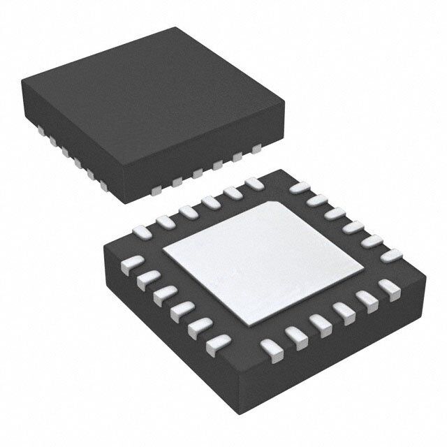
| 描述 | IC ATTENUATOR 4BIT SER/PAR 24QFN |
| 产品分类 | 衰减器 |
| 品牌 | Hittite Microwave Corporation |
| 数据手册 | 点击此处下载产品Datasheet |
| 产品图片 |  |
| 产品型号 | HMC629LP4E |
| rohs | 无铅 / 符合限制有害物质指令(RoHS)规范要求 |
| 产品系列 | - |
| 其它名称 | 1127-1496 1127-1496-1 1127-1496-ND |
| 功率(W) | - |
| 容差 | - |
| 封装/外壳 | 24-VQFN 裸露焊盘 |
| 标准包装 | 1 |
| 衰减值 | 3dB ~ 45dB |
| 阻抗 | 50 欧姆 |
| 频率范围 | 0 ~ 6GHz |
Datasheet
PDF Datasheet 数据手册内容提取
HMC629LP4 / 629LP4E v08.0112 3 dB LSB GaAs MMIC 4-BIT DIGITAL ATTENUATOR, DC - 6 GHz Typical Applications Features the HMC629lP4(e) is ideal for: 3 dB lsB steps to 45 dB t • Cellular/3G Infrastructure Power-up state selection M • WiBro / WiMAX / 4G low insertion loss: 2.5 dB s ttl/CMos Compatible, serial, ParEallel • Microwave Radio & VSAT - or latched Parallel Control l • Test Equipment and Sensors ±0.25 dB typical step error A • IF & RF Applications t Single +3V or +5V SupplTy i g 24 lead 4x4mm sMt Package: 16mm2 i D E - Functional Diagram General Description s r the HMC629lP4(e) is a broadband 4-bit gaAs iC L o Digital Attenuator in a low cost leadless sMt package. t this versatile digital attenuator incorporates off-chip A AC ground capacitors for near DC operation, making u O it suitable for a wide variety of rF and iF applications. n the dual mode control interface is CMos/ttl e compatible, and accepts either a three wire serial input t or a 4-bit parallel word. For applications which require t S A only 33 dB of attenuation range, the HMC629lP4(e) provides excellent attenuation accuracy up to 10 gHz. the HMC629lP4(e) is housed in a roHs compliant B 4x4 mm QFn leadless package, and requires no external matching components. O Electrical Specifications, T = +25° C, 50 Ohm System, with Vdd = +5V & Vctl = 0/+5V (Unless Otherwise Noted) A Parameter Frequency (gHz) Min. typ. Max. units dB insertion loss DC - 6 2.5 5 dB Attenuation range DC - 6 45 dB return loss (Attin, Attout, All Atten. states) DC - 6 17 dB Attenuation Accuracy: (referenced to insertion loss) dB ± (0.50 + 5% of Atten. setting) Max. All Attenuation states dB InFfoormra tpiorni cfuern,is hdeed lbivy eArnyal oag nDdev itcoes pisl abcelieev eodr dto ebres a: cHcuirtatteit ean dM reicliarbolew. Haovweev eCr, onor poFroart ipornic,e 2, dEelliivzearby,e atnhd D tor ivpela,c eC horedlemrss: fAonradl,o gM DAe v0ic1e8s2, 4Inc., responsibility is assumed by Analog Devices for its use, nor for any infringements of patents or other One Technology Way, P.O. Box 9106, Norwood, MA 02062-9106 1 rliicgehntss eo fi sth girrda nptaerdti ebsy t himatp mlicPaayht ioroens nuolret of:rto hm9er 7wits8is ue-s 2eu.n5 dS0epre- ca3infi3yc ap4tiao3tne sn ts ou rb Fjpeaactte xtno:t cr9higa7hnt8gs e-o 2wf Ai5thn0oaulo-t g3n oD3tiec7vei3.c eN s o. OPrhdoneer: O78n1--3li2n9e- 4a7t0 0w (cid:127)w Owrd.ehri totnitlein.ec aot mwww.analog.com Trademarks and registered trademarks aArep thpe lpircopaetrityo onf thSeiur rpesppeoctrivte: oPwhneorsn.e: 978-250-33A4p3p l icoart i oanp Spusp@pohrti:t Ptihteo.nceo: 1m-800-ANALOG-D
HMC629LP4 / 629LP4E v08.0112 3 dB LSB GaAs MMIC 4-BIT DIGITAL ATTENUATOR, DC - 6 GHz Normalized Attenuation Insertion Loss vs. Temperature (Only Major States are Shown) 0 0 dB) t B) -5 ON (-10 M N LOSS (d-10 TTENUATI--3200 E - s O A TI D l INSER-15 ++-428055 CCC MALIZE-40 T tA NOR-50 gi -20 -60 i D 0 2 4 6 8 10 0 2E 4 6 8 10 FREQUENCY (GHz) FREQUENCY (GHz) - s r Input Return Loss OutLput Return Loss o (Only Major States are Shown) (Only Major States are Shown) t 0 0 A -5 O -5 u n B) -10 B)-10 S (d -15 S (d-15 e S S t O O N L -20 S N L-20 t UR -25 UR-25 A T T E E R R -30 -30 -35 B -35 -40 -40 0 2 4 6 8 10 0 2 4 6 8 10 FREQUENCY (GHz) FREQUENCY (GHz) O Bit Error vs. Frequency Bit Error vs. Attenuation State (Only Major States are Shown) 10 6 8 (1, 2, 4, 5) GHz 4 6 B) 4 B) 2 d d R ( 2 R ( O O R 0 R 0 R R T E -2 T E BI -4 BI -2 BIT 24 (7, 8, 10) GHz -6 -4 -8 ALL BITS -10 -6 0 5 10 15 20 25 30 35 40 45 0 2 4 6 8 10 ATTENUATION STATE (dB) FREQUENCY (GHz) InFfoormra tpiorni cfuern,is hdeed lbivy eArnyal oag nDdev itcoes pisl abcelieev eodr dto ebres a: cHcuirtatteit ean dM reicliarbolew. Haovweev eCr, onor poFroart ipornic,e 2, dEelliivzearby,e atnhd D tor ivpela,c eC horedlemrss: fAonradl,o gM DAe v0ic1e8s2, 4Inc., responsibility is assumed by Analog Devices for its use, nor for any infringements of patents or other One Technology Way, P.O. Box 9106, Norwood, MA 02062-9106 rights of third parties that mPayh roesnulet f:ro m9 7its8 u-s2e.5 S0pe-c3ifi3ca4tio3n s s u bFjeact xto: c9ha7n8ge- 2wi5th0ou-t 3no3tic7e3. N o OPrhdoneer: O78n1--3li2n9e- 4a7t0 0w (cid:127)w Owrd.ehri totnitlein.ec aot mwww.analog.com 2 license is granted by implication or otherwise under any patent or patent rights of Analog Devices. Trademarks and registered trademarks aArep thpe lpircopaetrityo onf thSeiur rpesppeoctrivte: oPwhneorsn.e: 978-250-33A4p3p l icoart i oanp Spusp@pohrti:t Ptihteo.nceo: 1m-800-ANALOG-D
HMC629LP4 / 629LP4E v08.0112 3 dB LSB GaAs MMIC 4-BIT DIGITAL ATTENUATOR, DC - 6 GHz Step Error vs. Frequency Normal Relative Phase vs. Frequency (Only Major States are Shown) 2 100 24 dB 80 t 1.5 BIT (3, 6, 12) ALL BITS 45 dB sM R (dB) 0.51 SE (deg) 246000 E - ERRO 0 E PHA 0 l EP -0.5 TIV-20 A T A S L-40 t -1 RE T (3, 6, 12) dB i BIT 24 -60 g -1.5 -80 i -2 -100 D 0 2 4 6 8 10 0 1 2E3 4 5 6 7 8 9 10 - FREQUENCY (GHz) FREQUENCY (GHz) s r L o Serial Control Interface t the HMC629lP4e contains a 3-wire sPi compatible digital interface (serin, ClK, le). the serial control interface A u is activated when P/s is kept high. the 4-bit serial word mOust be loaded MsB first. the positive-edge sensitive ClK n and LE requires clean transitions. If mechanical switches are used, sufficient debouncing should be provided. When e LE is high, 4-bit data in the serial input register is transferred to the attenuator. When LE is high CLK is masked to t prevent data transition during output loading. t S When P/S is low, 3-wire SPI interface inputs (SERIN, CLK, LE) are disabled and the input register is loaded with A parallel digital inputs (D0-D5). When LE is high, 4-bit parallel data changes the state of the part per truth table. For all modes of operations, the state will stay constant while le is kept low. B O InFfoormra tpiorni cfuern,is hdeed lbivy eArnyal oag nDdev itcoes pisl abcelieev eodr dto ebres a: cHcuirtatteit ean dM reicliarbolew. Haovweev eCr, onor poFroart ipornic,e 2, dEelliivzearby,e atnhd D tor ivpela,c eC horedlemrss: fAonradl,o gM DAe v0ic1e8s2, 4Inc., responsibility is assumed by Analog Devices for its use, nor for any infringements of patents or other One Technology Way, P.O. Box 9106, Norwood, MA 02062-9106 3 rliicgehntss eo fi sth girrda nptaerdti ebsy t himatp mlicPaayht ioroens nuolret of:rto hm9er 7wits8is ue-s 2eu.n5 dS0epre- ca3infi3yc ap4tiao3tne sn ts ou rb Fjpeaactte xtno:t cr9higa7hnt8gs e-o 2wf Ai5thn0oaulo-t g3n oD3tiec7vei3.c eN s o. OPrhdoneer: O78n1--3li2n9e- 4a7t0 0w (cid:127)w Owrd.ehri totnitlein.ec aot mwww.analog.com Trademarks and registered trademarks aArep thpe lpircopaetrityo onf thSeiur rpesppeoctrivte: oPwhneorsn.e: 978-250-33A4p3p l icoart i oanp Spusp@pohrti:t Ptihteo.nceo: 1m-800-ANALOG-D
HMC629LP4 / 629LP4E v08.0112 3 dB LSB GaAs MMIC 4-BIT DIGITAL ATTENUATOR, DC - 6 GHz Parameter typ. Timing Diagram (Latched Parallel Mode) Min. serial period, t 100 ns sCK Control set-up time, t 20 ns Cs t Control hold-time, tCH 20 ns M le setup-time, t 10 ns ln E s Min. le pulse width, tLEW 10 ns - Min le pulse spacing, t 630 ns les l serial clock hold-time from le, tCKn 10 ns A Hold time, t 0 ns T t PH. i Latch Enable Minimum Width, t 10 ns g len setup time, tPs 2 ns Di E - Parallel Mode (Direct Parallel Mode & Latched Parallel Mode) s Note: the parallel mode is enabled when P/s is set to low. r L o Direct Parallel Mode - The attenuation state is changed by the Control Voltage Inputs directly. The LE (Latch Enable) t must be at a logic high to control the attenuator in this manner. A O u Latched Parallel Mode - The attenuation state is selected using the Control Voltage Inputs and set while the LE is in n the Low state. The attenuator will not change state while LE is Low. Once all Control Voltage Inputs are at the desired e states the le is pulsed. see timing diagram below for reference. t S t A Power-Up States PUP Truth Table If LE is set to logic LOW at power-up, the logic state of PuP1 and PuP2 determines the pBower-up state of the le PuP1 PuP2 Attenuation state part per PuP truth table. if the le is set to logic HigH 0 0 0 45 dB at power-up, the logic state of D3-D0 determines 0 1 0 45 dB the power-up state of the part per truth table. the 0 0 1 45 dB O attenuator latches in the desired power-up state 0 1 1 insertion loss approximately 200 ms after power-up. 1 X X 0 to 45 dB note: Power-up with le= 1 provides direct parallel operation with Power-On Sequence D0 - D3. The ideal power-up sequence is: GND, Vdd, digital Truth Table inputs, rF inputs. the relative order of the digital inputs are not important as long as they are powered Control Voltage Input Attenuation state after Vdd / GND D3 D2 D1 D0 reference High High High High Bias Voltage i.l. High High High low 3 dB Vdd (Vdc) idd (typ.) (mA) High High low High 6 dB 5 2.0 High low High High 12 dB Control Voltage Table low High High High 24 dB Any combination of the above states will provide an attenuation state Vdd = +3V Vdd = +5V approximately equal to the sum of the bits selected. low 0 to 0.5V @ <1 µA 0 to 0.8V @ <1 µA High 2 to 3V @ <1 µA 2 to 5V @ <1 µA InFfoormra tpiorni cfuern,is hdeed lbivy eArnyal oag nDdev itcoes pisl abcelieev eodr dto ebres a: cHcuirtatteit ean dM reicliarbolew. Haovweev eCr, onor poFroart ipornic,e 2, dEelliivzearby,e atnhd D tor ivpela,c eC horedlemrss: fAonradl,o gM DAe v0ic1e8s2, 4Inc., responsibility is assumed by Analog Devices for its use, nor for any infringements of patents or other One Technology Way, P.O. Box 9106, Norwood, MA 02062-9106 rights of third parties that mPayh roesnulet f:ro m9 7its8 u-s2e.5 S0pe-c3ifi3ca4tio3n s s u bFjeact xto: c9ha7n8ge- 2wi5th0ou-t 3no3tic7e3. N o OPrhdoneer: O78n1--3li2n9e- 4a7t0 0w (cid:127)w Owrd.ehri totnitlein.ec aot mwww.analog.com 4 license is granted by implication or otherwise under any patent or patent rights of Analog Devices. Trademarks and registered trademarks aArep thpe lpircopaetrityo onf thSeiur rpesppeoctrivte: oPwhneorsn.e: 978-250-33A4p3p l icoart i oanp Spusp@pohrti:t Ptihteo.nceo: 1m-800-ANALOG-D
HMC629LP4 / 629LP4E v08.0112 3 dB LSB GaAs MMIC 4-BIT DIGITAL ATTENUATOR, DC - 6 GHz Absolute Maximum Ratings rF input Power (DC - 6 gHz) 28 dBm (t = +85 °C) ELECTROSTATIC SENSITIVE DEVICE t Digital inputs (Data, shift Clock, -0.5 to Vdd +0.5V OBSERVE HANDLING PRECAUTIONS M Latch Enable & Serial Input) s Bias Voltage (Vdd) 5.6V E Channel temperature 150 °C - Continuous Pdiss (t = 85 °C) l 0.66 W (derate 10 mW/°C above 85 °C) [1] A t thermal resistance 98.5 °C/W T i storage temperature -65 to +150 °C g operating temperature -40 to +85 °C i D E - s Outline Drawing r L o t A u O n e t t S A B O notes: 1. leADFrAMe MAteriAl: CoPPer AlloY 2. DiMensions Are in inCHes [MilliMeters] 3. LEAD SPACING TOLERANCE IS NON-CUMULATIVE. 4. PAD BURR LENGTH SHALL BE 0.15mm MAXIMUM. PAD BURR HEIGHT SHALL BE 0.05mm MAXIMUM. 5. PACKAGE WARP SHALL NOT EXCEED 0.05mm. 6. All grounD leADs AnD grounD PADDle Must Be solDereD to PCB rF grounD. 7. reFer to PCB Design AnD AsseMBlY For QFn PACKAges APPliCAtion note For suggesteD lAnD PAttern. Package Information Part number Package Body Material lead Finish Msl rating Package Marking [3] HMC629lP4 low stress injection Molded Plastic sn/Pb solder Msl1 [1] H629 XXXX HMC629lP4e roHs-compliant low stress injection Molded Plastic 100% matte sn Msl1 [2] H629 XXXX [1] Max peak reflow temperature of 235 °C [2] Max peak reflow temperature of 260 °C [3] 4-Digit lot number XXXX InFfoormra tpiorni cfuern,is hdeed lbivy eArnyal oag nDdev itcoes pisl abcelieev eodr dto ebres a: cHcuirtatteit ean dM reicliarbolew. Haovweev eCr, onor poFroart ipornic,e 2, dEelliivzearby,e atnhd D tor ivpela,c eC horedlemrss: fAonradl,o gM DAe v0ic1e8s2, 4Inc., responsibility is assumed by Analog Devices for its use, nor for any infringements of patents or other One Technology Way, P.O. Box 9106, Norwood, MA 02062-9106 5 rliicgehntss eo fi sth girrda nptaerdti ebsy t himatp mlicPaayht ioroens nuolret of:rto hm9er 7wits8is ue-s 2eu.n5 dS0epre- ca3infi3yc ap4tiao3tne sn ts ou rb Fjpeaactte xtno:t cr9higa7hnt8gs e-o 2wf Ai5thn0oaulo-t g3n oD3tiec7vei3.c eN s o. OPrhdoneer: O78n1--3li2n9e- 4a7t0 0w (cid:127)w Owrd.ehri totnitlein.ec aot mwww.analog.com Trademarks and registered trademarks aArep thpe lpircopaetrityo onf thSeiur rpesppeoctrivte: oPwhneorsn.e: 978-250-33A4p3p l icoart i oanp Spusp@pohrti:t Ptihteo.nceo: 1m-800-ANALOG-D
HMC629LP4 / 629LP4E v08.0112 3 dB LSB GaAs MMIC 4-BIT DIGITAL ATTENUATOR, DC - 6 GHz Pin Descriptions Pin number Function Description interface schematic t 24 P/s M 1 ClK E s - 2 serin l see truth table, control voltage A table and timing diagram. T t i g 3 le i D E - s these pins and package bottom 4, 15 gnD r must be connected to rFL/DC ground. o t these pins are DC coupled and matched to 50 ohms. A Attin, 5, 14 Attout Blocking capacitors Oare required. select value based u on lowest frequency of operation. n e external capacitors to ground are required. select value for t 6 - 13 ACg1 - ACg6 lowest frequency of operation. Place capacitor as close to Spins as possible. see Application Circuit. t A B 16 serout serial input data delayed by 6 clock cycles. O 17, 18 PuP2, PuP1 see truth table, control voltage table and timing diagram. 20 - 23 D3, D2, D1, D0 19 Vdd supply voltage InFfoormra tpiorni cfuern,is hdeed lbivy eArnyal oag nDdev itcoes pisl abcelieev eodr dto ebres a: cHcuirtatteit ean dM reicliarbolew. Haovweev eCr, onor poFroart ipornic,e 2, dEelliivzearby,e atnhd D tor ivpela,c eC horedlemrss: fAonradl,o gM DAe v0ic1e8s2, 4Inc., responsibility is assumed by Analog Devices for its use, nor for any infringements of patents or other One Technology Way, P.O. Box 9106, Norwood, MA 02062-9106 rights of third parties that mPayh roesnulet f:ro m9 7its8 u-s2e.5 S0pe-c3ifi3ca4tio3n s s u bFjeact xto: c9ha7n8ge- 2wi5th0ou-t 3no3tic7e3. N o OPrhdoneer: O78n1--3li2n9e- 4a7t0 0w (cid:127)w Owrd.ehri totnitlein.ec aot mwww.analog.com 6 license is granted by implication or otherwise under any patent or patent rights of Analog Devices. Trademarks and registered trademarks aArep thpe lpircopaetrityo onf thSeiur rpesppeoctrivte: oPwhneorsn.e: 978-250-33A4p3p l icoart i oanp Spusp@pohrti:t Ptihteo.nceo: 1m-800-ANALOG-D
HMC629LP4 / 629LP4E v08.0112 3 dB LSB GaAs MMIC 4-BIT DIGITAL ATTENUATOR, DC - 6 GHz Application Circuit t M s E - l A t T i g i D E - s r L o t A u O n e t t S A B O InFfoormra tpiorni cfuern,is hdeed lbivy eArnyal oag nDdev itcoes pisl abcelieev eodr dto ebres a: cHcuirtatteit ean dM reicliarbolew. Haovweev eCr, onor poFroart ipornic,e 2, dEelliivzearby,e atnhd D tor ivpela,c eC horedlemrss: fAonradl,o gM DAe v0ic1e8s2, 4Inc., responsibility is assumed by Analog Devices for its use, nor for any infringements of patents or other One Technology Way, P.O. Box 9106, Norwood, MA 02062-9106 7 rliicgehntss eo fi sth girrda nptaerdti ebsy t himatp mlicPaayht ioroens nuolret of:rto hm9er 7wits8is ue-s 2eu.n5 dS0epre- ca3infi3yc ap4tiao3tne sn ts ou rb Fjpeaactte xtno:t cr9higa7hnt8gs e-o 2wf Ai5thn0oaulo-t g3n oD3tiec7vei3.c eN s o. OPrhdoneer: O78n1--3li2n9e- 4a7t0 0w (cid:127)w Owrd.ehri totnitlein.ec aot mwww.analog.com Trademarks and registered trademarks aArep thpe lpircopaetrityo onf thSeiur rpesppeoctrivte: oPwhneorsn.e: 978-250-33A4p3p l icoart i oanp Spusp@pohrti:t Ptihteo.nceo: 1m-800-ANALOG-D
HMC629LP4 / 629LP4E v08.0112 3 dB LSB GaAs MMIC 4-BIT DIGITAL ATTENUATOR, DC - 6 GHz Evaluation PCB t M E s - l A T t i g i D E - s r L o t A O u n e t S t A B O List of Materials for Evaluation PCB 118889 [1] the circuit board used in the application should use item Description rF circuit design techniques. signal lines should J1, J2 PCB Mount sMA Connector have 50 ohm impedance while the package ground J10, J12 DC Pin leads and exposed paddle should be connected J11 18 Pin DC Connector directly to the ground plane similar to that shown. C1 - C2 100 pF, capacitor 0402 pkg A sufficient number of via holes should be used to C3 1000 pF, capacitor 0402 pkg connect the top and bottom ground planes. the C4 - C8 330 pF, capacitor 0402 pkg evaluation circuit board shown is available from Hit- r1 - r10 100 kohm resistor, 0402 Pkg. tite upon request. SW1 sPDt 4 Position DiP switch u1 HMC629lP4(e) Digital Attenuator PCB [2] 118888 evaluation PCB [1] reference this number when ordering complete evaluation PCB [2] Circuit Board Material: Arlon 25Fr InFfoormra tpiorni cfuern,is hdeed lbivy eArnyal oag nDdev itcoes pisl abcelieev eodr dto ebres a: cHcuirtatteit ean dM reicliarbolew. Haovweev eCr, onor poFroart ipornic,e 2, dEelliivzearby,e atnhd D tor ivpela,c eC horedlemrss: fAonradl,o gM DAe v0ic1e8s2, 4Inc., responsibility is assumed by Analog Devices for its use, nor for any infringements of patents or other One Technology Way, P.O. Box 9106, Norwood, MA 02062-9106 rights of third parties that mPayh roesnulet f:ro m9 7its8 u-s2e.5 S0pe-c3ifi3ca4tio3n s s u bFjeact xto: c9ha7n8ge- 2wi5th0ou-t 3no3tic7e3. N o OPrhdoneer: O78n1--3li2n9e- 4a7t0 0w (cid:127)w Owrd.ehri totnitlein.ec aot mwww.analog.com 8 license is granted by implication or otherwise under any patent or patent rights of Analog Devices. Trademarks and registered trademarks aArep thpe lpircopaetrityo onf thSeiur rpesppeoctrivte: oPwhneorsn.e: 978-250-33A4p3p l icoart i oanp Spusp@pohrti:t Ptihteo.nceo: 1m-800-ANALOG-D