首页 > HMC575LP4E > 详情
 Datasheet下载
- 型号: HMC575LP4E
- 制造商: Hittite
- 库位|库存: xxxx|xxxx
- 要求:
| 数量阶梯 | 香港交货 | 国内含税 |
| +xxxx | $xxxx | ¥xxxx |
查看当月历史价格
查看今年历史价格
产品参数
| 参数 | 数值 |
| 产品目录 | 射频/IF 和 RFID |
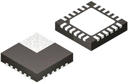
| 描述 | IC MULTIPLIER X2 24-QFN |
| 产品分类 | RF 其它 IC 和模块 |
| 品牌 | Hittite Microwave Corporation |
| 数据手册 | 点击此处下载产品Datasheet |
| 产品图片 |  |
| 产品型号 | HMC575LP4E |
| RF类型 | 通用 |
| rohs | 无铅 / 符合限制有害物质指令(RoHS)规范要求 |
| 产品系列 | - |
| 供应商器件封装 | 24-QFN(4x4) |
| 其它名称 | 1127-1464 1127-1464-1 1127-1464-ND |
| 功能 | 频率系数 |
| 包装 | 剪切带 (CT) |
| 封装/外壳 | 24-VQFN 裸露焊盘 |
| 标准包装 | 1 |
| 辅助属性 | 有源倍频器 |
| 频率 | 6GHz ~ 9GHz |
Datasheet
PDF Datasheet 数据手册内容提取
HMC575LP4 / 575LP4E v00.0506 SMT GaAs MMIC x2 ACTIVE FREQUENCY MULTIPLIER, 6 - 9 GHz OUTPUT Typical Applications Features 7 The HMC575LP4 / HMC575LP4E is suitable for: High Output Power: +17 dBm • Wireless Local Loop Low Input Power Drive: -2 to +6 dBm • Point-to-Point & VSAT Radios Fo, 3Fo Isolation: 15 dBc T • Test Instrumentation 100 KHz SSB Phase Noise: -140 dBc/Hz M S • Military & Space Single Supply: +5V@ 90 mA - RoHS Compliant 4x4 mm SMT Package E V I T Functional Diagram General Description C A The HMC575LP4 & HMC575LP4E are x2 active broadband frequency multipliers utilizing GaAs - S PHEMT technology in a leadless RoHS compliant R SMT package. When driven by a 3 dBm signal, the E multiplier provides +17 dBm typical output power from I 6 to 9 GHz. The Fo and 3Fo isolations are 15 dBc with L P respect to output signal level. This frequency multiplier I features DC blocked I/O’s, and is ideal for use in LO T L multiplier chains for Pt to Pt & VSAT Radios yielding U reduced parts count vs. traditional approaches. The low M additive SSB Phase Noise of -140 dBc/Hz at 100 kHz offset helps maintain good system noise performance. . Q The HMC575LP4 & HMC575LP4E are compatible with E surface mount manufacturing techniques. R F Electrical Specifi cations, T = +25° C, Vdd1, Vdd2 = +5V, 3 dBm Drive Level A Parameter Min. Typ. Max. Units Frequency Range, Input 3 - 4.5 GHz Frequency Range, Output 6 - 9 GHz Output Power 14 17 dBm Fo Isolation (with respect to output level) 15 dBc 3Fo Isolation (with respect to output level) 15 dBc Input Return Loss 15 dB Output Return Loss 12 dB SSB Phase Noise (100 kHz Offset) -140 dBc/Hz Supply Current (Idd1 & Idd2) 90 mA Information furnisheFd obry Apnrailcoge D, edviceelsi vise breylie,v eadn tdo bteo a cpcluaractee a nod rrdelieabrlse., Hpowleevaers, eno coFnotra pcritc eH, idtteiltieve rMy, iacnrdo wtoa pvlaec eC oorrdperosr: aAtnioalnog: Devices, Inc., responsibility is assumed by Analog Devices for its use, nor for any infringements of patents or other One Technology Way, P.O. Box 9106, Norwood, MA 02062-9106 7 - 94 rights of third parties tha2t 0ma yA relpsuhlt faro mR itos uasde. ,S pCechifiecaltmionss fsoubrjedct, toM chAan g0e1 w8ith2ou4t nPotihceo. Nnoe : P9h7o8n-e2: 75801--332394-437 0 0F (cid:127)a Ox:r d9e7r o8n-l2in5e 0at- w33w7w3.analog.com license is granted by implication or otherwise under any patent or patent rights of Analog Devices. Trademarks and registered trademarks are the property of their resOpercdtivee orw Onerns.-line at www.hAiptptilticea.tcioonm Support: Phone: 1-800-ANALOG-D
HMC575LP4 / 575LP4E v00.0506 SMT GaAs MMIC x2 ACTIVE FREQUENCY MULTIPLIER, 6 - 9 GHz OUTPUT Output Power vs. Temperature @ 3 dBm Drive Level Output Power vs. Drive Level 7 25 25 20 m) 20 m) B B 15 d d WER ( 15 WER ( 10 MT O O UT P 10 ++2855CC UT P 5 - 02ddBBmm S OUTP -40C OUTP 0 246dddBBBmmm - 5 E -5 V 0 -10 I 5.5 6 6.5 7 7.5 8 8.5 9 9.5 6 6.5 7 7.5 8 8.5 9 T C OUTPUT FREQUENCY (GHz) FREQUENCY (GHz) A - Output Power vs. S Supply Voltage @ 3 dBm Drive Level Isolation @ 3 dBm Drive Level R 25 25 E 20 I L m) 20 m) 15 P B B ER (d 15 ER (d 10 Fo TI W W 2Fo L O O 5 3Fo PUT P 10 VVVdddddd===455...505VVV PUT P 0 MU T T OU OU -5 5 . -10 Q E 0 -15 6 6.5 7 7.5 8 8.5 9 6 6.5 7 7.5 8 8.5 9 R OUTPUT FREQUENCY (GHz) OUTPUT FREQUENCY (GHz) F Output Power vs. Input Power 25 20 m) 15 B d R ( 10 E W O 5 P T PU 0 6 GHz T 7.5GHz OU -5 9 GHz -10 -15 -10 -8 -6 -4 -2 0 2 4 6 8 10 INPUT POWER (dBm) Information furnisheFd obry Apnrailcoge D, edviceelsi vise breylie,v eadn tdo bteo a cpcluaractee a nod rrdelieabrlse., Hpowleevaers, eno coFnotra pcritc eH, idtteiltieve rMy, iacnrdo wtoa pvlaec eC oorrdperosr: aAtnioalnog: Devices, Inc., responsibility is assumed by Analog Devices for its use, nor for any infringements of patents or other One Technology Way, P.O. Box 9106, Norwood, MA 02062-9106 rights of third parties tha2t 0ma yA relpsuhlt faro mR itos uasde. ,S pCechifiecaltmionss fsoubrjedct, toM chAan g0e1 w8ith2ou4t nPotihceo. Nnoe : P9h7o8n-e2: 75801--332394-437 0 0F (cid:127)a Ox:r d9e7r o8n-l2in5e 0at- w33w7w3.analog.com 7 - 95 license is granted by implication or otherwise under any patent or patent rights of Analog Devices. Trademarks and registered trademarks are the property of their resOpercdtivee orw Onerns.-line at www.hAiptptilticea.tcioonm Support: Phone: 1-800-ANALOG-D
HMC575LP4 / 575LP4E v00.0506 SMT GaAs MMIC x2 ACTIVE FREQUENCY MULTIPLIER, 6 - 9 GHz OUTPUT Input Return Loss vs. Temperature Output Return Loss vs. Temperature 7 0 0 -2 B) -5 dB) -4 MT N LOSS (d -10 ++-428055CCC RN LOSS ( --86 ++-428055CCC R U -10 U T S ET -15 RE -12 - UT R PUT -14 E INP -20 OUT -16 V -18 I -25 -20 T 3 3.25 3.5 3.75 4 4.25 4.5 6 6.5 7 7.5 8 8.5 9 C FREQUENCY (GHz) FREQUENCY (GHz) A - S Absolute Maximum Ratings Typical Supply Current vs. Vdd R E RF Input (Vdd = +5V) +13 dBm Vdd (Vdc) Idd (mA) I Supply Voltage (Vdd) +6.0 Vdc 4.5 89 L P Channel Temperature 150 °C 5.0 90 I Continuous Pdiss (T= 85 °C) 5.5 91 T 512 mW (derate 7.9 mW/°C above 85 °C) L Note: U Thermal Resistance 127 °C/W Multiplier will operate over full voltage range shown above. (channel to ground paddle) M Storage Temperature -65 to +150 °C . Operating Temperature -40 to +85 °C Q ELECTROSTATIC SENSITIVE DEVICE E OBSERVE HANDLING PRECAUTIONS R F Information furnisheFd obry Apnrailcoge D, edviceelsi vise breylie,v eadn tdo bteo a cpcluaractee a nod rrdelieabrlse., Hpowleevaers, eno coFnotra pcritc eH, idtteiltieve rMy, iacnrdo wtoa pvlaec eC oorrdperosr: aAtnioalnog: Devices, Inc., responsibility is assumed by Analog Devices for its use, nor for any infringements of patents or other One Technology Way, P.O. Box 9106, Norwood, MA 02062-9106 7 - 96 rights of third parties tha2t 0ma yA relpsuhlt faro mR itos uasde. ,S pCechifiecaltmionss fsoubrjedct, toM chAan g0e1 w8ith2ou4t nPotihceo. Nnoe : P9h7o8n-e2: 75801--332394-437 0 0F (cid:127)a Ox:r d9e7r o8n-l2in5e 0at- w33w7w3.analog.com license is granted by implication or otherwise under any patent or patent rights of Analog Devices. Trademarks and registered trademarks are the property of their resOpercdtivee orw Onerns.-line at www.hAiptptilticea.tcioonm Support: Phone: 1-800-ANALOG-D
HMC575LP4 / 575LP4E v00.0506 SMT GaAs MMIC x2 ACTIVE FREQUENCY MULTIPLIER, 6 - 9 GHz OUTPUT Outline Drawing 7 T M S - E V I T C A - S R E I L NOTES: P 1. LEADFRAME MATERIAL: COPPER ALLOY I 2. DIMENSIONS ARE IN INCHES [MILLIMETERS] T L 3. LEAD SPACING TOLERANCE IS NON-CUMULATIVE. 4. PAD BURR LENGTH SHALL BE 0.15mm MAXIMUM. U PAD BURR HEIGHT SHALL BE 0.05mm MAXIMUM. M 5. PACKAGE WARP SHALL NOT EXCEED 0.05mm. 6. ALL GROUND LEADS AND GROUND PADDLE MUST BE . SOLDERED TO PCB RF GROUND. Q 7. REFER TO HITTITE APPLICATION NOT FOR SUGGESTED E LAND PATTERN. R F Package Information Part Number Package Body Material Lead Finish MSL Rating Package Marking [3] HMC575LP4 Low Stress Injection Molded Plastic Sn/Pb Solder MSL1 [1] H575 XXXX HMC575LP4E RoHS-compliant Low Stress Injection Molded Plastic 100% matte Sn MSL1 [2] H575 XXXX [1] Max peak refl ow temperature of 235 °C [2] Max peak refl ow temperature of 260 °C [3] 4-Digit lot number XXXX Information furnisheFd obry Apnrailcoge D, edviceelsi vise breylie,v eadn tdo bteo a cpcluaractee a nod rrdelieabrlse., Hpowleevaers, eno coFnotra pcritc eH, idtteiltieve rMy, iacnrdo wtoa pvlaec eC oorrdperosr: aAtnioalnog: Devices, Inc., responsibility is assumed by Analog Devices for its use, nor for any infringements of patents or other One Technology Way, P.O. Box 9106, Norwood, MA 02062-9106 rights of third parties tha2t 0ma yA relpsuhlt faro mR itos uasde. ,S pCechifiecaltmionss fsoubrjedct, toM chAan g0e1 w8ith2ou4t nPotihceo. Nnoe : P9h7o8n-e2: 75801--332394-437 0 0F (cid:127)a Ox:r d9e7r o8n-l2in5e 0at- w33w7w3.analog.com 7 - 97 license is granted by implication or otherwise under any patent or patent rights of Analog Devices. Trademarks and registered trademarks are the property of their resOpercdtivee orw Onerns.-line at www.hAiptptilticea.tcioonm Support: Phone: 1-800-ANALOG-D
HMC575LP4 / 575LP4E v00.0506 SMT GaAs MMIC x2 ACTIVE FREQUENCY MULTIPLIER, 6 - 9 GHz OUTPUT Pin Description 7 Pin Number Function Description Interface Schematic These pins are internally not connected; however, 1, 5 - 14, 18, N/C this product was specifi ed with these pins connected 19, 21, 23, 24 to RF/ DC ground. T M Package bottom must also be connected 2, 4, 15, 17 GND S to RF/DC ground. - Pin is AC coupled and matched E 3 RFIN to 50 Ohms from 3 - 4.5 GHz. V I T Pin is AC coupled and matched 16 RFOUT C to 50 Ohms from 6 - 9 GHz. A - S Supply voltage 5V ± 0.5V. External bypass capacitors 20, 22 Vdd2, Vdd1 R of 100 pF and 2.2 μF are required. E I L P I T L Application Circuit U M Component Value Q. C1, C2 100 pF E C3, C4 2.2 μF R F Information furnisheFd obry Apnrailcoge D, edviceelsi vise breylie,v eadn tdo bteo a cpcluaractee a nod rrdelieabrlse., Hpowleevaers, eno coFnotra pcritc eH, idtteiltieve rMy, iacnrdo wtoa pvlaec eC oorrdperosr: aAtnioalnog: Devices, Inc., responsibility is assumed by Analog Devices for its use, nor for any infringements of patents or other One Technology Way, P.O. Box 9106, Norwood, MA 02062-9106 7 - 98 rights of third parties tha2t 0ma yA relpsuhlt faro mR itos uasde. ,S pCechifiecaltmionss fsoubrjedct, toM chAan g0e1 w8ith2ou4t nPotihceo. Nnoe : P9h7o8n-e2: 75801--332394-437 0 0F (cid:127)a Ox:r d9e7r o8n-l2in5e 0at- w33w7w3.analog.com license is granted by implication or otherwise under any patent or patent rights of Analog Devices. Trademarks and registered trademarks are the property of their resOpercdtivee orw Onerns.-line at www.hAiptptilticea.tcioonm Support: Phone: 1-800-ANALOG-D
HMC575LP4 / 575LP4E v00.0506 SMT GaAs MMIC x2 ACTIVE FREQUENCY MULTIPLIER, 6 - 9 GHz OUTPUT Evaluation PCB 7 T M S - E V I T C A - S R E I L P I T L U M . Q E R F List of Materials for Evaluation PCB 112405 [1] The circuit board used in the fi nal application should Item Description be generated with proper RF circuit design tech- J1, J2 PCB Mount SRI SMA Connector niques. Signal lines should have 50 ohm imped- J3 - J5 DC Pin ance while the package ground leads and exposed C1, C2 100 pF Capacitor, 0402 Pkg. paddle should be connected directly to the ground C3, C4 2.2 μF Tantalum Capacitor plane similar to that shown. The evaluation circuit HMC575LP4 / HMC575LP4E U1 x2 Active Multiplier board shown is available from Hittite upon request. PCB [2] 115270 Eval Board [1] Reference this number when ordering complete evaluation PCB [2] Circuit Board Material: Rogers 4350 Information furnisheFd obry Apnrailcoge D, edviceelsi vise breylie,v eadn tdo bteo a cpcluaractee a nod rrdelieabrlse., Hpowleevaers, eno coFnotra pcritc eH, idtteiltieve rMy, iacnrdo wtoa pvlaec eC oorrdperosr: aAtnioalnog: Devices, Inc., responsibility is assumed by Analog Devices for its use, nor for any infringements of patents or other One Technology Way, P.O. Box 9106, Norwood, MA 02062-9106 rights of third parties tha2t 0ma yA relpsuhlt faro mR itos uasde. ,S pCechifiecaltmionss fsoubrjedct, toM chAan g0e1 w8ith2ou4t nPotihceo. Nnoe : P9h7o8n-e2: 75801--332394-437 0 0F (cid:127)a Ox:r d9e7r o8n-l2in5e 0at- w33w7w3.analog.com 7 - 99 license is granted by implication or otherwise under any patent or patent rights of Analog Devices. Trademarks and registered trademarks are the property of their resOpercdtivee orw Onerns.-line at www.hAiptptilticea.tcioonm Support: Phone: 1-800-ANALOG-D
Mouser Electronics Authorized Distributor Click to View Pricing, Inventory, Delivery & Lifecycle Information: A nalog Devices Inc.: HMC575LP4E HMC575LP4 HMC575LP4ETR 112405-HMC575LP4 HMC575LP4TR