首页 > HMC532LP4E > 详情
 Datasheet下载
- 型号: HMC532LP4E
- 制造商: Hittite
- 库位|库存: xxxx|xxxx
- 要求:
| 数量阶梯 | 香港交货 | 国内含税 |
| +xxxx | $xxxx | ¥xxxx |
查看当月历史价格
查看今年历史价格
产品参数
| 参数 | 数值 |
| 产品目录 | 射频/IF 和 RFID |
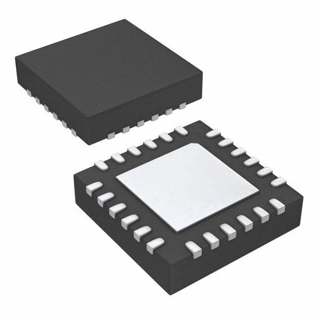
| 描述 | IC MMIC AMP VCO HBT GAAS 24-QFN |
| 产品分类 | RF 其它 IC 和模块 |
| 品牌 | Hittite Microwave Corporation |
| 数据手册 | 点击此处下载产品Datasheet |
| 产品图片 |  |
| 产品型号 | HMC532LP4E |
| RF类型 | 通用 |
| rohs | 无铅 / 符合限制有害物质指令(RoHS)规范要求 |
| 产品系列 | - |
| 供应商器件封装 | 24-QFN(4x4) |
| 其它名称 | 1127-1449 |
| 功能 | VCO,缓冲放大器 |
| 包装 | 散装 |
| 封装/外壳 | 24-VQFN 裸露焊盘 |
| 标准包装 | 100 |
| 辅助属性 | - |
| 频率 | 7.1GHz ~ 7.9GHz |
Datasheet
PDF Datasheet 数据手册内容提取
HMC532LP4 532LP4E / v01.0508 MMIC VCO w/ BUFFER AMPLIFIER, 7.1 - 7.9 GHz Typical Applications Features Low noise MMIC VCO w/Buffer Amplifi er for: Pout: +14 dBm • VSAT Radio Phase Noise: -103 dBc/Hz @100 KHz • Point to Point/Multipoint Radio No External Resonator Needed • Test Equipment & Industrial Controls Single Supply: +3V @ 85 mA • Military End-Use 24 Lead 4x4mm QFN Package: 9 mm2 Functional Diagram General Description The HMC532LP4 & HMC532LP4E are GaAs InGaP Heterojunction Bipolar Transistor (HBT) MMIC VCOs with integrated resonators, negative resistance 12 devices, varactor diodes, and buffer amplifi ers. Covering 7.1 to 7.9 GHz, the VCO’s phase noise performance is excellent over temperature, shock and vibration due to the oscillator’s monolithic struc- T ture. Power output is +14 dBm typical from a single M supply of +3V @ 85 mA. The voltage controlled S oscillator is packaged in a leadless QFN 4 x 4 mm - surface mount package. S O C V Electrical Specifi cations, T = +25° C, Vcc = +3V A Parameter Min. Typ. Max. Units Frequency Range 7.1 - 7.9 GHz Power Output 12 14 17 dBm SSB Phase Noise @ 100 kHz Offset, Vtune= +5V @ RF Output -101 dBc/Hz Tune Voltage (Vtune) 1 13 V Supply Current (Icc) (Vcc = +3V) 60 85 100 mA Tune Port Leakage Current 10 μA Output Return Loss 15 dB Harmonics 2nd -14 dBc 3rd -25 dBc Pulling (into a 2.0:1 VSWR) 28 MHz pp Pushing @ Vtune= +5V 78 MHz/V Frequency Drift Rate 0.85 MHz/°C Information furnisheFd obry Apnrailcoge D, edviceelsi vise breylie,v eadn tdo bteo a cpcluaractee a nod rrdelieabrlse., Hpowleevaers, eno coFnotra pcritc eH, idtteiltieve rMy, iacnrdo wtoa pvlaec eC oorrdperosr: aAtnioalnog: Devices, Inc., responsibility is assumed by Analog Devices for its use, nor for any infringements of patents or other One Technology Way, P.O. Box 9106, Norwood, MA 02062-9106 12 - 146 rights of third parties tha2t 0ma yA relpsuhlt faro mR itos uasde. ,S pCechifiecaltmionss fsoubrjedct, toM chAan g0e1 w8ith2ou4t nPotihceo. Nnoe : P9h7o8n-e2: 75801--332394-437 0 0F (cid:127)a Ox:r d9e7r o8n-l2in5e 0at- w33w7w3.analog.com license is granted by implication or otherwise under any patent or patent rights of Analog Devices. Trademarks and registered trademarks are the property of their resOpercdtivee orw Onerns.-line at www.hAiptptilticea.tcioonm Support: Phone: 1-800-ANALOG-D
HMC532LP4 / 532LP4E v01.0508 MMIC VCO w/ BUFFER AMPLIFIER, 7.1 - 7.9 GHz Frequency vs. Tuning Voltage, T= 25°C Frequency vs. Tuning Voltage, Vcc= +3V 8.5 8.5 8 8 z) z) H 7.5 H 7.5 G G Y ( Y ( C C N 7 N 7 E E U U Q 2.85V Q +25C RE 6.5 3.00V RE 6.5 +85C F 3.15V F -40C 6 6 5.5 5.5 0 1 2 3 4 5 6 7 8 9 10 11 12 13 0 1 2 3 4 5 6 7 8 9 10 11 12 13 TUNING VOLTAGE (VOLTS) TUNING VOLTAGE (VOLTS) Output Power vs. 12 Sensitivity vs. Tuning Voltage, Vcc= +3V Tuning Voltage, Vcc= +3V 600 20 500 18 LT) m) T Y (MHz/VO 340000 ++-428055CCC OWER (dB 1146 SM VIT T P 12 - SENSITI 200 OUTPU 10 ++2855CC OS 100 8 -40C C 0 6 V 0 1 2 3 4 5 6 7 8 9 10 11 12 13 0 1 2 3 4 5 6 7 8 9 10 11 12 13 TUNING VOLTAGE (VOLTS) TUNING VOLTAGE (VOLTS) Phase Noise vs. Tuning Voltage Typical SSB Phase Noise @ Vtune= +5V 0 0 -20 z) -20 z) H H Bc/ Bc/ -40 +25C d -40 10kHz offset d +85C E ( 100kHz offset E ( -60 -40C S S NOI -60 NOI -80 E E HAS -80 HAS-100 P P B B -120 S S S-100 S -140 -120 -160 0 1 2 3 4 5 6 7 8 9 10 11 12 13 103 104 105 106 107 TUNING VOLTAGE (VOLTS) OFFSET FREQUENCY (Hz) Information furnisheFd obry Apnrailcoge D, edviceelsi vise breylie,v eadn tdo bteo a cpcluaractee a nod rrdelieabrlse., Hpowleevaers, eno coFnotra pcritc eH, idtteiltieve rMy, iacnrdo wtoa pvlaec eC oorrdperosr: aAtnioalnog: Devices, Inc., responsibility is assumed by Analog Devices for its use, nor for any infringements of patents or other One Technology Way, P.O. Box 9106, Norwood, MA 02062-9106 rights of third parties tha2t 0ma yA relpsuhlt faro mR itos uasde. ,S pCechifiecaltmionss fsoubrjedct, toM chAan g0e1 w8ith2ou4t nPotihceo. Nnoe : P9h7o8n-e2: 75801--332394-437 0 0F (cid:127)a Ox:r d9e7r o8n-l2in5e 0at- w33w7w3.analog.com 12 - 147 license is granted by implication or otherwise under any patent or patent rights of Analog Devices. Trademarks and registered trademarks are the property of their resOpercdtivee orw Onerns.-line at www.hAiptptilticea.tcioonm Support: Phone: 1-800-ANALOG-D
HMC532LP4 / 532LP4E v01.0508 MMIC VCO w/ BUFFER AMPLIFIER, 7.1 - 7.9 GHz Absolute Maximum Ratings Typical Supply Current vs. Vcc Vcc +3.5 Vdc Vcc (V) Icc (mA) Vtune 0 to +15V 2.75 74 Channel Temperature 135 °C 3.0 85 Continuous Pdiss (T = 85°C) 3.25 96 303 mW (derate 6.07 mW/°C above 85°C) Note: VCO will operate over full voltage range shown above. Thermal Resistance 165 °C/W (junction to ground paddle) Storage Temperature -65 to +150 °C ELECTROSTATIC SENSITIVE DEVICE Operating Temperature -40 to +85 °C OBSERVE HANDLING PRECAUTIONS ESD Sensitivity (HBM) Class 1A Outline Drawing 12 T M S - S O C V NOTES: 1. LEADFRAME MATERIAL: COPPER ALLOY 2. DIMENSIONS ARE IN INCHES [MILLIMETERS] 3. LEAD SPACING TOLERANCE IS NON-CUMULATIVE. 4. PAD BURR LENGTH SHALL BE 0.15mm MAXIMUM. PAD BURR HEIGHT SHALL BE 0.05mm MAXIMUM. 5. PACKAGE WARP SHALL NOT EXCEED 0.05mm. 6. ALL GROUND LEADS AND GROUND PADDLE MUST BE SOLDERED TO PCB RF GROUND. 7. REFER TO HITTITE APPLICATION NOT FOR SUGGESTED LAND PATTERN. Package Information Part Number Package Body Material Lead Finish MSL Rating Package Marking [3] HMC532LP4 Low Stress Injection Molded Plastic Sn/Pb Solder MSL1 [1] H532 XXXX HMC532LP4E RoHS-compliant Low Stress Injection Molded Plastic 100% matte Sn MSL1 [2] H532 XXXX [1] Max peak refl ow temperature of 235 °C [2] Max peak refl ow temperature of 260 °C [3] 4-Digit lot number XXXX Information furnisheFd obry Apnrailcoge D, edviceelsi vise breylie,v eadn tdo bteo a cpcluaractee a nod rrdelieabrlse., Hpowleevaers, eno coFnotra pcritc eH, idtteiltieve rMy, iacnrdo wtoa pvlaec eC oorrdperosr: aAtnioalnog: Devices, Inc., responsibility is assumed by Analog Devices for its use, nor for any infringements of patents or other One Technology Way, P.O. Box 9106, Norwood, MA 02062-9106 12 - 148 rights of third parties tha2t 0ma yA relpsuhlt faro mR itos uasde. ,S pCechifiecaltmionss fsoubrjedct, toM chAan g0e1 w8ith2ou4t nPotihceo. Nnoe : P9h7o8n-e2: 75801--332394-437 0 0F (cid:127)a Ox:r d9e7r o8n-l2in5e 0at- w33w7w3.analog.com license is granted by implication or otherwise under any patent or patent rights of Analog Devices. Trademarks and registered trademarks are the property of their resOpercdtivee orw Onerns.-line at www.hAiptptilticea.tcioonm Support: Phone: 1-800-ANALOG-D
HMC532LP4 / 532LP4E v01.0508 MMIC VCO w/ BUFFER AMPLIFIER, 7.1 - 7.9 GHz Pin Descriptions Pin Number Function Description Interface Schematic 1- 14, 17 - 19, N/C No Connection 21, 23, 24 This pin must be connected to RF & DC ground. Package bottom 15 GND has an exposed metal paddle that must be RF & DC grounded. 16 RFOUT RF output (AC coupled) 20 Vcc Supply Voltage Vcc= 3V Control Voltage Input. Modulation port bandwidth 12 22 VTUNE dependent on drive source impedance. See “Determining the FM Bandwidth of a Wideband Varactor Tuned VCO” application note. T Evaluation PCB M S - S O C V List of Materials for Evaluation PCB 105706 [1] The circuit board used in the fi nal application should Item Description use RF circuit design techniques. Signal lines J1 - J2 PCB Mount SMA RF Connector should have 50 ohm impedance while the package J3 - J4 DC Pin ground leads and exposed paddle should be con- C1 4.7 μF Tantalum Capacitor nected directly to the ground plane similar to that C2 10,000 pF Capacitor, 0603 Pkg. shown. A sufficient number of via holes should be U1 HMC532LP4 / HMC532LP4E VCO used to connect the top and bottom ground planes. PCB [2] 105667 Eval Board The evaluation circuit board shown is available from [1] Reference this number when ordering complete evaluation PCB Hittite upon request. [2] Circuit Board Material: Rogers 4350 Information furnisheFd obry Apnrailcoge D, edviceelsi vise breylie,v eadn tdo bteo a cpcluaractee a nod rrdelieabrlse., Hpowleevaers, eno coFnotra pcritc eH, idtteiltieve rMy, iacnrdo wtoa pvlaec eC oorrdperosr: aAtnioalnog: Devices, Inc., responsibility is assumed by Analog Devices for its use, nor for any infringements of patents or other One Technology Way, P.O. Box 9106, Norwood, MA 02062-9106 rights of third parties tha2t 0ma yA relpsuhlt faro mR itos uasde. ,S pCechifiecaltmionss fsoubrjedct, toM chAan g0e1 w8ith2ou4t nPotihceo. Nnoe : P9h7o8n-e2: 75801--332394-437 0 0F (cid:127)a Ox:r d9e7r o8n-l2in5e 0at- w33w7w3.analog.com 12 - 149 license is granted by implication or otherwise under any patent or patent rights of Analog Devices. Trademarks and registered trademarks are the property of their resOpercdtivee orw Onerns.-line at www.hAiptptilticea.tcioonm Support: Phone: 1-800-ANALOG-D