首页 > HMC513LP5E > 详情
 Datasheet下载
- 型号: HMC513LP5E
- 制造商: Hittite
- 库位|库存: xxxx|xxxx
- 要求:
| 数量阶梯 | 香港交货 | 国内含税 |
| +xxxx | $xxxx | ¥xxxx |
查看当月历史价格
查看今年历史价格
产品参数
| 参数 | 数值 |
| 产品目录 | 射频/IF 和 RFID |
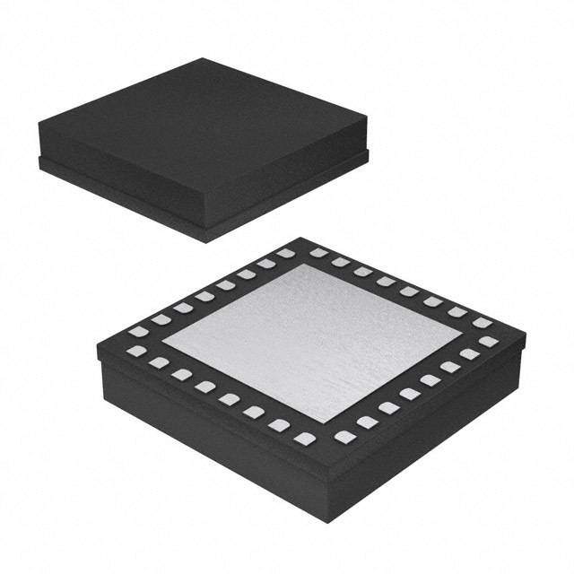
| 描述 | IC MMIC AMP VCO HBT 2OUT 32-QFN |
| 产品分类 | RF 其它 IC 和模块 |
| 品牌 | Hittite Microwave Corporation |
| 数据手册 | 点击此处下载产品Datasheet |
| 产品图片 |  |
| 产品型号 | HMC513LP5E |
| RF类型 | 通用 |
| rohs | 无铅 / 符合限制有害物质指令(RoHS)规范要求 |
| 产品系列 | - |
| 供应商器件封装 | 32-SMT (5x5) |
| 其它名称 | 1127-1442 1127-1442-1 1127-1442-ND |
| 功能 | VCO |
| 包装 | 剪切带 (CT) |
| 封装/外壳 | 32-TFQFN 裸露焊盘 |
| 标准包装 | 1 |
| 辅助属性 | 三路输出(除以 2,除以 4,标准) |
| 频率 | 10.43GHz ~ 11.46GHz |
Datasheet
PDF Datasheet 数据手册内容提取
HMC513LP5 513LP5E / v04.0811 MMIC VCO w/ HALF FREQUENCY OUTPUT & DIVIDE-BY-4, 10.43 - 11.46 GHz Typical Applications Features Low noise MMIC VCO w/Half Frequency, Divide-by-4 Dual Output: Fo = 10.43 - 11.46 GHz Outputs for: Fo/2 = 5.21 - 5.73 GHz • VSAT Radio Pout: +7 dBm • Point to Point/Multipoint Radio Phase Noise: -110 dBc/Hz @100 KHz Typ. • Test Equipment & Industrial Controls No External Resonator Needed • Military End-Use 32 Lead 5x5mm SMT Package: 25mm² Functional Diagram General Description The HMC513LP5 & HMC513LP5E are GaAs InGaP Heterojunction Bipolar Transistor (HBT) MMIC VCOs. The HMC513LP5 & HMC513LP5E integrate resonators, negative resistance devices, varactor diodes and feature half frequency and divide-by- 4 outputs. The VCO’s phase noise performance is excellent over temperature, shock, and process due to 8 the oscillator’s monolithic structure. Power output is +7 dBm typical from a +3V supply voltage. The prescaler function can be disabled to conserve current if not T required. The voltage controlled oscillator is packaged M in a leadless QFN 5x5 mm surface mount package, S and requires no external matching components. - T U P Electrical Specifications, T = +25° C, Vcc1, Vcc2 = +3V T A U Parameter Min. Typ. Max. Units O Fo 10.43 - 11.46 GHz Frequency Range Fo/2 5.215 - 5.73 GHz 2 / RFOUT +5 +10 dBm o Power Output RFOUT/2 +5 +11 dBm F RFOUT/4 -10 -4 dBm h SSB Phase Noise @ 100 kHz Offset, Vtune= +5V @ RFOUT -110 dBc/Hz t Tune Voltage Vtune 2 13 V i w Supply Current Icc1 & Icc2 240 275 290 mA S Tune Port Leakage Current (Vtune= 13V) 10 µA O Output Return Loss 2 dB C Harmonics/Subharmonics 1/2 32 dBc V 3/2 26 dBc 2nd 15 dBc 3rd 28 dBc Pulling (into a 2.0:1 VSWR) 5 MHz pp Pushing @ Vtune= 5V 25 MHz/V Frequency Drift Rate 1 MHz/°C InforFmaotiro np fruircniseh,e dd beyl iAvnealroyg Daenvidce st ois pbelaliecveed otor dbee arcsc:u rHateit taintde reMliaibcler. oHwowaevveer, Cnoo rpFoorr aptriiocen,, d2e0liv Aerlyp, haand R too apdla,c Ce horedlemrss: fAonrdal,o gM DAe v0ic1e8s2, 4Inc., responsibility is assumed by Analog Devices for its use, nor for any infringements of patents or other One Technology Way, P.O. Box 9106, Norwood, MA 02062-9106 8 - 1 rliicgehntss eo fi sth girrda nptaerdti ebsy t himatp mlicaaPyt iorhenso uonlrt ofertoh:m e9r wit7sis 8ues -eu2.n dS5ep0re ca-inf3iyc 3aptia4otne3sn ts ou rb jpeFacttae tnoxt c:r hig9ahn7tgs 8eo wf- 2Aithn5oau0lot g-n 3oDti3ecve7i.c 3eNso . POhrodnee:r 7 O81n-3-l2i9n-e4 7a0t0 w(cid:127) wOrwde.hr oitntliitnee. cato wmww.analog.com Trademarks and registered trademarks arAe tphep plriocpearttyi oof nth eSir urepsppecotivret :o wPnehrso.ne: 978-250-3A3p4p3li c aotrio na Spuppsp@orht: iPtthitoen.ec: o1-m800-ANALOG-D
HMC513LP5 / 513LP5E v04.0811 MMIC VCO w/ HALF FREQUENCY OUTPUT & DIVIDE-BY-4, 10.43 - 11.46 GHz Frequency vs. Tuning Voltage, T= 25°C Frequency vs. Tuning Voltage, Vcc= +3V 11.8 11.8 z)11.4 z)11.4 H H G G Y ( Y ( C 11 C 11 N N E E U U Q10.6 Q10.6 E E R R F F UT 10.2 VVcccc==23..705VV UT 10.2 ++2855 CC P Vcc=3.25V P -40 C T T U U O 9.8 O 9.8 9.4 9.4 0 1 2 3 4 5 6 7 8 9 10 11 12 13 0 1 2 3 4 5 6 7 8 9 10 11 12 13 TUNING VOLTAGE (VOLTS) TUNING VOLTAGE (VOLTS) Output Power Sensitivity vs. Tuning Voltage, Vcc= +3V vs. Tuning Voltage, Vcc= +3V 600 15 8 MHz/VOLT)450000 ++-428055 CCC WER (dBm) 192 ++-428055 CCC Y (300 O T T P SITIVI200 TPUT 6 M N U S E O S 3 100 - T 0 0 0 1 2 3 4 5 6 7 8 9 10 11 12 13 0 1 2 3 4 5 6 7 8 9 10 11 12 13 U TUNING VOLTAGE (VOLTS) TUNING VOLTAGE (VOLTS) P T U O SSB Phase Noise vs. Tuning Voltage SSB Phase Noise @ Vtune= +5V 2 -70 0 / -75 -20 o Hz)-80 Hz) F dBc/-85 dBc/-40 ++2855 CC h SE (-90 SE (-60 -40 C t NOI-95 NOI-80 wi ASE -100 11000kkHHzz o offfsfseett ASE -100 S H H B P-105 B P-120 O S-110 S S S C -115 -140 V -120 -160 1 2 3 4 5 6 7 8 9 10 11 12 13 103 104 105 106 107 TUNING VOLTAGE (VOLTS) OFFSET FREQUENCY (Hz) InforFmaotiro np fruircniseh,e dd beyl iAvnealroyg Daenvidce st ois pbelaliecveed otor dbee arcsc:u rHateit taintde reMliaibcler. oHwowaevveer, Cnoo rpFoorr aptriiocen,, d2e0liv Aerlyp, haand R too apdla,c Ce horedlemrss: fAonrdal,o gM DAe v0ic1e8s2, 4Inc., responsibility is assumed by Analog Devices for its use, nor for any infringements of patents or other One Technology Way, P.O. Box 9106, Norwood, MA 02062-9106 rights of third parties that maPy rhesounlt fero:m 9 it7s 8us-e2. S5p0ec-if3ic3ati4on3s s u b jeFcta tox c: h9an7g8e w-2ith5ou0t -n3oti3ce7. 3No POhrodnee:r 7 O81n-3-l2i9n-e4 7a0t0 w(cid:127) wOrwde.hr oitntliitnee. cato wmww.analog.com 8 - 2 license is granted by implication or otherwise under any patent or patent rights of Analog Devices. Trademarks and registered trademarks arAe tphep plriocpearttyi oof nth eSir urepsppecotivret :o wPnehrso.ne: 978-250-3A3p4p3li c aotrio na Spuppsp@orht: iPtthitoen.ec: o1-m800-ANALOG-D
HMC513LP5 / 513LP5E v04.0811 MMIC VCO w/ HALF FREQUENCY OUTPUT & DIVIDE-BY-4, 10.43 - 11.46 GHz RFOUT/2 Frequency RFOUT/2 Output Power vs. Tuning Voltage, Vcc= +3V vs. Tuning Voltage, Vcc= +3V 5.9 15 z) 5.7 GH m) 12 ENCY ( 5.5 ER (dB 9 U W Q 5.3 O E P TPUT FR 5.1 ++2855 CC OUTPUT 6 ++2855 CC OU 4.9 -40 C 3 -40 C 4.7 0 0 1 2 3 4 5 6 7 8 9 10 11 12 13 0 1 2 3 4 5 6 7 8 9 10 11 12 13 TUNING VOLTAGE (VOLTS) TUNING VOLTAGE (VOLTS) Divide-by-4 Frequency Divide-by-4 Output Power vs. Tuning Voltage, Vcc= +3V vs. Tuning Voltage, Vcc= +3V 2.95 0 8 z)2.85 GH m) -3 ENCY (2.75 ER (dB -6 U W T EQ2.65 PO SM UTPUT FR2.55 ++-428055 CCC OUTPUT -1-29 ++-428055 CCC O2.45 - T 2.35 -15 U 0 1 2 3 4 5 6 7 8 9 10 11 12 13 0 1 2 3 4 5 6 7 8 9 10 11 12 13 P TUNING VOLTAGE (VOLTS) TUNING VOLTAGE (VOLTS) T U O Absolute Maximum Ratings Typical Supply Current vs. Vcc 2 / Vcc1, Vcc2 +3.5 Vdc Vcc (V) Icc (mA) o Vtune 0 to +15V 2.75 230 F Junction Temperature 135 °C 3.0 275 h Continuous Pdiss (T=85 °C) 3.25 320 t 1.3 W i (derate 27 mW/C above 85 °C Note: VCO will operate over full voltage range shown above. w Thermal Resistance 37.5 °C/W S (junction to ground paddle) ELECTROSTATIC SENSITIVE DEVICE O Storage Temperature -65 to +150 °C OBSERVE HANDLING PRECAUTIONS C Operating Temperature -40 to +85 °C V InforFmaotiro np fruircniseh,e dd beyl iAvnealroyg Daenvidce st ois pbelaliecveed otor dbee arcsc:u rHateit taintde reMliaibcler. oHwowaevveer, Cnoo rpFoorr aptriiocen,, d2e0liv Aerlyp, haand R too apdla,c Ce horedlemrss: fAonrdal,o gM DAe v0ic1e8s2, 4Inc., responsibility is assumed by Analog Devices for its use, nor for any infringements of patents or other One Technology Way, P.O. Box 9106, Norwood, MA 02062-9106 8 - 3 rliicgehntss eo fi sth girrda nptaerdti ebsy t himatp mlicaaPyt iorhenso uonlrt ofertoh:m e9r wit7sis 8ues -eu2.n dS5ep0re ca-inf3iyc 3aptia4otne3sn ts ou rb jpeFacttae tnoxt c:r hig9ahn7tgs 8eo wf- 2Aithn5oau0lot g-n 3oDti3ecve7i.c 3eNso . POhrodnee:r 7 O81n-3-l2i9n-e4 7a0t0 w(cid:127) wOrwde.hr oitntliitnee. cato wmww.analog.com Trademarks and registered trademarks arAe tphep plriocpearttyi oof nth eSir urepsppecotivret :o wPnehrso.ne: 978-250-3A3p4p3li c aotrio na Spuppsp@orht: iPtthitoen.ec: o1-m800-ANALOG-D
HMC513LP5 / 513LP5E v04.0811 MMIC VCO w/ HALF FREQUENCY OUTPUT & DIVIDE-BY-4, 10.43 - 11.46 GHz Outline Drawing NOTES: 1. LEADFRAME MATERIAL: COPPER ALLOY 2. DIMENSIONS ARE IN INCHES [MILLIMETERS] 3. LEAD SPACING TOLERANCE IS NON-CUMULATIVE. 8 4. PAD BURR LENGTH SHALL BE 0.15mm MAXIMUM. PAD BURR HEIGHT SHALL BE 0.05mm MAXIMUM. 5. PACKAGE WARP SHALL NOT EXCEED 0.05mm. 6. ALL GROUND LEADS AND GROUND PADDLE MUST BE SOLDERED TO PCB RF GROUND. T Package Information 7. REFER TO HITTITE APPLICATION NOTE FOR SUGGESTED LAND PATTERN. M Part Number Package Body Material Lead Finish MSL Rating Package Marking [3] S HMC513LP5 Low Stress Injection Molded Plastic Sn/Pb Solder MSL3 [1] XHX5X13X - HMC513LP5E RoHS-compliant Low Stress Injection Molded Plastic 100% matte Sn MSL3 [2] H513 T XXXX U [1] Max peak reflow temperature of 235 °C P [2] Max peak reflow temperature of 260 °C T [3] 4-Digit lot number XXXX U O Pin Descriptions 2 Pin Number Function Description Interface Schematic / o 1 - 3, 7 - 10, No Connection. These pins may be connected to RF/ F 13 - 18, 20, N/C DC ground. Performance will not be affected. 22 - 28, 30 - 32 h t i w 4 RFOUT/4 Divide-by-4 Output S O C V Supply Voltage for prescaler. If prescaler is not 6 VCC1 required, this pin may be left open to conserve 40 mA of current. InforFmaotiro np fruircniseh,e dd beyl iAvnealroyg Daenvidce st ois pbelaliecveed otor dbee arcsc:u rHateit taintde reMliaibcler. oHwowaevveer, Cnoo rpFoorr aptriiocen,, d2e0liv Aerlyp, haand R too apdla,c Ce horedlemrss: fAonrdal,o gM DAe v0ic1e8s2, 4Inc., responsibility is assumed by Analog Devices for its use, nor for any infringements of patents or other One Technology Way, P.O. Box 9106, Norwood, MA 02062-9106 rights of third parties that maPy rhesounlt fero:m 9 it7s 8us-e2. S5p0ec-if3ic3ati4on3s s u b jeFcta tox c: h9an7g8e w-2ith5ou0t -n3oti3ce7. 3No POhrodnee:r 7 O81n-3-l2i9n-e4 7a0t0 w(cid:127) wOrwde.hr oitntliitnee. cato wmww.analog.com 8 - 4 license is granted by implication or otherwise under any patent or patent rights of Analog Devices. Trademarks and registered trademarks arAe tphep plriocpearttyi oof nth eSir urepsppecotivret :o wPnehrso.ne: 978-250-3A3p4p3li c aotrio na Spuppsp@orht: iPtthitoen.ec: o1-m800-ANALOG-D
HMC513LP5 / 513LP5E v04.0811 MMIC VCO w/ HALF FREQUENCY OUTPUT & DIVIDE-BY-4, 10.43 - 11.46 GHz Pin Descriptions Pin Number Function Description Interface Schematic 12 RFOUT/2 Half frequency output (AC coupled). 19 RFOUT RF output (AC coupled). 21 VCC2 Supply Voltage, +3V Control Voltage Input. Modulation port bandwidth 29 VTUNE dependent on drive source impedance. 8 Package bottom has an exposed metal paddle 5, 11, Paddle GND that must be connected to RF/DC ground. T M S Typical Application Circuit - T U P T U O 2 / o F h t i w S O C V InforFmaotiro np fruircniseh,e dd beyl iAvnealroyg Daenvidce st ois pbelaliecveed otor dbee arcsc:u rHateit taintde reMliaibcler. oHwowaevveer, Cnoo rpFoorr aptriiocen,, d2e0liv Aerlyp, haand R too apdla,c Ce horedlemrss: fAonrdal,o gM DAe v0ic1e8s2, 4Inc., responsibility is assumed by Analog Devices for its use, nor for any infringements of patents or other One Technology Way, P.O. Box 9106, Norwood, MA 02062-9106 8 - 5 rliicgehntss eo fi sth girrda nptaerdti ebsy t himatp mlicaaPyt iorhenso uonlrt ofertoh:m e9r wit7sis 8ues -eu2.n dS5ep0re ca-inf3iyc 3aptia4otne3sn ts ou rb jpeFacttae tnoxt c:r hig9ahn7tgs 8eo wf- 2Aithn5oau0lot g-n 3oDti3ecve7i.c 3eNso . POhrodnee:r 7 O81n-3-l2i9n-e4 7a0t0 w(cid:127) wOrwde.hr oitntliitnee. cato wmww.analog.com Trademarks and registered trademarks arAe tphep plriocpearttyi oof nth eSir urepsppecotivret :o wPnehrso.ne: 978-250-3A3p4p3li c aotrio na Spuppsp@orht: iPtthitoen.ec: o1-m800-ANALOG-D
HMC513LP5 / 513LP5E v04.0811 MMIC VCO w/ HALF FREQUENCY OUTPUT & DIVIDE-BY-4, 10.43 - 11.46 GHz Evaluation PCB 8 T M S - T U P T U O List of Materials for Evaluation PCB 110227 [1] The circuit board used in the final application 2 Item Description / should use RF circuit design techniques. Signal o J1 - J4 PCB Mount SMA RF Connector lines should have 50 Ohm impedance while the F J5 - J6 2 mm DC Header package ground leads and backside ground paddle h C1 - C3 100 pF Capacitor, 0402 Pkg. t should be connected directly to the ground plane C4 1,000 pF Capacitor, 0402 Pkg. wi similar to that shown. A sufficient number of via C5 - C7 2.2 µF Tantalum Capacitor holes should be used to connect the top and bottom S U1 HMC513LP5(E) VCO ground planes. The evaluation circuit board shown O PCB [2] 110225 Eval Board is available from Hittite upon request. C [1] Reference this number when ordering complete evaluation PCB V [2] Circuit Board Material: Arlon 25FR InforFmaotiro np fruircniseh,e dd beyl iAvnealroyg Daenvidce st ois pbelaliecveed otor dbee arcsc:u rHateit taintde reMliaibcler. oHwowaevveer, Cnoo rpFoorr aptriiocen,, d2e0liv Aerlyp, haand R too apdla,c Ce horedlemrss: fAonrdal,o gM DAe v0ic1e8s2, 4Inc., responsibility is assumed by Analog Devices for its use, nor for any infringements of patents or other One Technology Way, P.O. Box 9106, Norwood, MA 02062-9106 rights of third parties that maPy rhesounlt fero:m 9 it7s 8us-e2. S5p0ec-if3ic3ati4on3s s u b jeFcta tox c: h9an7g8e w-2ith5ou0t -n3oti3ce7. 3No POhrodnee:r 7 O81n-3-l2i9n-e4 7a0t0 w(cid:127) wOrwde.hr oitntliitnee. cato wmww.analog.com 8 - 6 license is granted by implication or otherwise under any patent or patent rights of Analog Devices. Trademarks and registered trademarks arAe tphep plriocpearttyi oof nth eSir urepsppecotivret :o wPnehrso.ne: 978-250-3A3p4p3li c aotrio na Spuppsp@orht: iPtthitoen.ec: o1-m800-ANALOG-D