首页 > HMC508LP5E > 详情
 Datasheet下载
- 型号: HMC508LP5E
- 制造商: Hittite
- 库位|库存: xxxx|xxxx
- 要求:
| 数量阶梯 | 香港交货 | 国内含税 |
| +xxxx | $xxxx | ¥xxxx |
查看当月历史价格
查看今年历史价格
产品参数
| 参数 | 数值 |
| 产品目录 | 射频/IF 和 RFID |
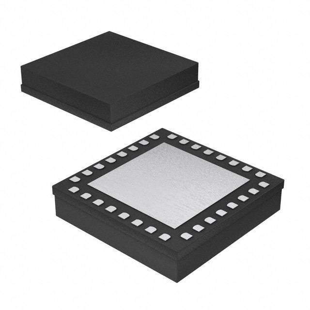
| 描述 | IC MMIC AMP VCO HBT 2OUT 32-QFN |
| 产品分类 | RF 其它 IC 和模块 |
| 品牌 | Hittite Microwave Corporation |
| 数据手册 | 点击此处下载产品Datasheet |
| 产品图片 |  |
| 产品型号 | HMC508LP5E |
| RF类型 | 通用 |
| rohs | 无铅 / 符合限制有害物质指令(RoHS)规范要求 |
| 产品系列 | - |
| 供应商器件封装 | 32-SMT (5x5) |
| 其它名称 | 1127-1437 |
| 功能 | VCO |
| 包装 | 剪带 |
| 封装/外壳 | 32-TQFN 裸露焊盘 |
| 标准包装 | 50 |
| 辅助属性 | 双输出(除以 2,标准) |
| 频率 | 7.3GHz ~ 8.2GHz |
Datasheet
PDF Datasheet 数据手册内容提取
HMC508LP5 508LP5E / v04.0811 MMIC VCO w/ HALF FREQUENCY OUTPUT 7.3 - 8.2 GHz Typical Applications Features Low noise MMIC VCO w/Half Frequency, for: Dual Output: Fo = 7.3 - 8.2 GHz Fo/2 = 3.65 - 4.1 GHz • VSAT Radio Pout: +15.0 dBm • Point to Point/Multi-Point Radio Phase Noise: -116 dBc/Hz @100 kHz Typ. • Test Equipment & Industrial Controls No External Resonator Needed • Military End-Use 32 Lead 5x5mm SMT Package: 25mm² Functional Diagram General Description The HMC508LP5 & HMC508LP5E are GaAs InGaP Heterojunction Bipolar Transistor (HBT) MMIC VCOs. The HMC508LP5 & HMC508LP5E integrate resonators, negative resistance devices, varactor diodes and feature a half frequency output. The VCO’s phase noise performance is excellent over temper- ature, shock, and process due to the oscillator’s 8 monolithic structure. Power output is +15 dBm typical from a +5V supply. The voltage controlled oscillator is packaged in a leadless QFN 5x5 mm surface T mount package, and requires no external matching M components. S - T U P Electrical Specifications, T = +25° C, Vcc = +5V T A U Parameter Min. Typ. Max. Units O Fo 7.3 - 8.2 GHz Frequency Range Fo/2 3.65 - 4.1 GHz 2 / RFOUT +12 +17 dBm o Power Output RFOUT/2 +4 +10 dBm F SSB Phase Noise @ 100 kHz Offset, Vtune= +5V @ RFOUT -116 dBc/Hz h Tune Voltage Vtune 2 13 V t i Supply Current (Icc) (Vcc = +5.0V) 200 240 280 mA w Tune Port Leakage Current (Vtune= 13V) 10 µA S Output Return Loss 2 dB O Harmonics/Subharmonics 1/2 40 dBc C 2nd 20 dBc V 3rd 35 dBc Pulling (into a 2.0:1 VSWR) 8 MHz pp Pushing @ Vtune= 5V 10 MHz/V Frequency Drift Rate 1.0 MHz/°C InforFmaotiro np fruircniseh,e dd beyl iAvnealroyg Daenvidce st ois pbelaliecveed otor dbee arcsc:u rHateit taintde reMliaibcler. oHwowaevveer, Cnoo rpFoorr aptriiocen,, d2e0liv Aerlyp, haand R too apdla,c Ce horedlemrss: fAonrdal,o gM DAe v0ic1e8s2, 4Inc., responsibility is assumed by Analog Devices for its use, nor for any infringements of patents or other One Technology Way, P.O. Box 9106, Norwood, MA 02062-9106 8 - 1 rliicgehntss eo fi sth girrda nptaerdti ebsy t himatp mlicaaPyt iorhenso uonlrt ofertoh:m e9r wit7sis 8ues -eu2.n dS5ep0re ca-inf3iyc 3aptia4otne3sn ts ou rb jpeFacttae tnoxt c:r hig9ahn7tgs 8eo wf- 2Aithn5oau0lot g-n 3oDti3ecve7i.c 3eNso . POhrodnee:r 7 O81n-3-l2i9n-e4 7a0t0 w(cid:127) wOrwde.hr oitntliitnee. cato wmww.analog.com Trademarks and registered trademarks arAe tphep plriocpearttyi oof nth eSir urepsppecotivret :o wPnehrso.ne: 978-250-3A3p4p3li c aotrio na Spuppsp@orht: iPtthitoen.ec: o1-m800-ANALOG-D
HMC508LP5 / 508LP5E v04.0811 MMIC VCO w/ HALF FREQUENCY OUTPUT 7.3 - 8.2 GHz Frequency vs. Tuning Voltage, T= 25°C Frequency vs. Tuning Voltage, Vcc= +5V 9 9 z) 8.5 z) 8.5 H H G G CY ( 8 CY ( 8 N N E E U U Q 7.5 Q 7.5 E E R R F F UT 7 VVcccc==45..705VV UT 7 ++2855 CC P Vcc=5.25V P -40 C T T U U O 6.5 O 6.5 6 6 0 1 2 3 4 5 6 7 8 9 10 11 12 13 0 1 2 3 4 5 6 7 8 9 10 11 12 13 TUNING VOLTAGE (VOLTS) TUNING VOLTAGE (VOLTS) Output Power Sensitivity vs. Tuning Voltage, Vcc= +5V vs. Tuning Voltage, Vcc= +5V 600 20 8 500 Y (MHz/V)400 ++-428055 CCC WER (dBm) 1126 VIT300 PO +25 C T SENSITI200 OUTPUT 8 +-4805 CC SM 4 100 - T 0 0 0 1 2 3 4 5 6 7 8 9 10 11 12 13 0 1 2 3 4 5 6 7 8 9 10 11 12 13 U TUNING VOLTAGE (VOLTS) TUNING VOLTAGE (VOLTS) P T U O SSB Phase Noise vs. Tuning Voltage SSB Phase Noise @ Vtune = +5V 2 -10 0 / o -20 z)-30 z) F H H Bc/ Bc/-40 +25 C E (d-50 11000kkHHzz o offfsfseett E (d-60 +-4805 CC th S S NOI-70 NOI-80 wi SE SE A A-100 S H-90 H B P B P-120 O S S S-110 S C -140 V -130 -160 1 2 3 4 5 6 7 8 9 10 11 12 13 102 103 104 105 106 TUNING VOLTAGE (VOLTS) OFFSET FREQUENCY (Hz) InforFmaotiro np fruircniseh,e dd beyl iAvnealroyg Daenvidce st ois pbelaliecveed otor dbee arcsc:u rHateit taintde reMliaibcler. oHwowaevveer, Cnoo rpFoorr aptriiocen,, d2e0liv Aerlyp, haand R too apdla,c Ce horedlemrss: fAonrdal,o gM DAe v0ic1e8s2, 4Inc., responsibility is assumed by Analog Devices for its use, nor for any infringements of patents or other One Technology Way, P.O. Box 9106, Norwood, MA 02062-9106 rights of third parties that maPy rhesounlt fero:m 9 it7s 8us-e2. S5p0ec-if3ic3ati4on3s s u b jeFcta tox c: h9an7g8e w-2ith5ou0t -n3oti3ce7. 3No POhrodnee:r 7 O81n-3-l2i9n-e4 7a0t0 w(cid:127) wOrwde.hr oitntliitnee. cato wmww.analog.com 8 - 2 license is granted by implication or otherwise under any patent or patent rights of Analog Devices. Trademarks and registered trademarks arAe tphep plriocpearttyi oof nth eSir urepsppecotivret :o wPnehrso.ne: 978-250-3A3p4p3li c aotrio na Spuppsp@orht: iPtthitoen.ec: o1-m800-ANALOG-D
HMC508LP5 / 508LP5E v04.0811 MMIC VCO w/ HALF FREQUENCY OUTPUT 7.3 - 8.2 GHz RFOUT/2 Frequency RFOUT/2 Output Power vs. Tuning Voltage, Vcc= +5V vs. Tuning Voltage, Vcc= +5V 4.5 12 z)4.25 10 GH m) NCY ( 4 R (dB 8 E E U W Q3.75 O 6 E P OUTPUT FR3.32.55 ++-428055 CCC OUTPUT 24 ++-428055 CCC 3 0 0 1 2 3 4 5 6 7 8 9 10 11 12 13 0 1 2 3 4 5 6 7 8 9 10 11 12 13 TUNING VOLTAGE (VOLTS) TUNING VOLTAGE (VOLTS) Absolute Maximum Ratings Typical Supply Current vs. Vcc Vcc +5.5 Vdc Vcc (V) Icc (mA) 8 Vtune 0 to +15V 4.75 220 Junction Temperature 135 °C 5.0 240 Continuous Pdiss (T=85 °C) 5.25 260 1.4 W (derate 28 mW/C above 85 °C Note: VCO will operate over full voltage range shown above. T Thermal Resistance 35 °C/W M (junction to ground paddle) ELECTROSTATIC SENSITIVE DEVICE S Storage Temperature -65 to +150 °C OBSERVE HANDLING PRECAUTIONS Operating Temperature -40 to +85 °C - ESD Sensitivity (HBM) Class 1A T U P T U O 2 / o F h t i w S O C V InforFmaotiro np fruircniseh,e dd beyl iAvnealroyg Daenvidce st ois pbelaliecveed otor dbee arcsc:u rHateit taintde reMliaibcler. oHwowaevveer, Cnoo rpFoorr aptriiocen,, d2e0liv Aerlyp, haand R too apdla,c Ce horedlemrss: fAonrdal,o gM DAe v0ic1e8s2, 4Inc., responsibility is assumed by Analog Devices for its use, nor for any infringements of patents or other One Technology Way, P.O. Box 9106, Norwood, MA 02062-9106 8 - 3 rliicgehntss eo fi sth girrda nptaerdti ebsy t himatp mlicaaPyt iorhenso uonlrt ofertoh:m e9r wit7sis 8ues -eu2.n dS5ep0re ca-inf3iyc 3aptia4otne3sn ts ou rb jpeFacttae tnoxt c:r hig9ahn7tgs 8eo wf- 2Aithn5oau0lot g-n 3oDti3ecve7i.c 3eNso . POhrodnee:r 7 O81n-3-l2i9n-e4 7a0t0 w(cid:127) wOrwde.hr oitntliitnee. cato wmww.analog.com Trademarks and registered trademarks arAe tphep plriocpearttyi oof nth eSir urepsppecotivret :o wPnehrso.ne: 978-250-3A3p4p3li c aotrio na Spuppsp@orht: iPtthitoen.ec: o1-m800-ANALOG-D
HMC508LP5 / 508LP5E v04.0811 MMIC VCO w/ HALF FREQUENCY OUTPUT 7.3 - 8.2 GHz Outline Drawing 8 NOTES: T 1. LEADFRAME MATERIAL: COPPER ALLOY 2. DIMENSIONS ARE IN INCHES [MILLIMETERS] M 3. LEAD SPACING TOLERANCE IS NON-CUMULATIVE. S 4. PAD BURR LENGTH SHALL BE 0.15mm MAXIMUM. PAD BURR HEIGHT SHALL BE 0.05mm MAXIMUM. - 5. PACKAGE WARP SHALL NOT EXCEED 0.05mm. T 6. ALL GROUND LEADS AND GROUND PADDLE MUST BE U SOLDERED TO PCB RF GROUND. 7. REFER TO HITTITE APPLICATION NOTE FOR SUGGESTED P LAND PATTERN. T U O Package Information 2 / o Part Number Package Body Material Lead Finish MSL Rating Package Marking [3] F HMC508LP5 Low Stress Injection Molded Plastic Sn/Pb Solder MSL3 [1] XHX5X08X h t HMC508LP5E RoHS-compliant Low Stress Injection Molded Plastic 100% matte Sn MSL3 [2] XHX5X08X wi [1] Max peak reflow temperature of 235 °C S [2] Max peak reflow temperature of 260 °C O [3] 4-Digit lot number XXXX C V InforFmaotiro np fruircniseh,e dd beyl iAvnealroyg Daenvidce st ois pbelaliecveed otor dbee arcsc:u rHateit taintde reMliaibcler. oHwowaevveer, Cnoo rpFoorr aptriiocen,, d2e0liv Aerlyp, haand R too apdla,c Ce horedlemrss: fAonrdal,o gM DAe v0ic1e8s2, 4Inc., responsibility is assumed by Analog Devices for its use, nor for any infringements of patents or other One Technology Way, P.O. Box 9106, Norwood, MA 02062-9106 rights of third parties that maPy rhesounlt fero:m 9 it7s 8us-e2. S5p0ec-if3ic3ati4on3s s u b jeFcta tox c: h9an7g8e w-2ith5ou0t -n3oti3ce7. 3No POhrodnee:r 7 O81n-3-l2i9n-e4 7a0t0 w(cid:127) wOrwde.hr oitntliitnee. cato wmww.analog.com 8 - 4 license is granted by implication or otherwise under any patent or patent rights of Analog Devices. Trademarks and registered trademarks arAe tphep plriocpearttyi oof nth eSir urepsppecotivret :o wPnehrso.ne: 978-250-3A3p4p3li c aotrio na Spuppsp@orht: iPtthitoen.ec: o1-m800-ANALOG-D
HMC508LP5 / 508LP5E v04.0811 MMIC VCO w/ HALF FREQUENCY OUTPUT 7.3 - 8.2 GHz Pin Descriptions Pin Number Function Description Interface Schematic 1 - 4, 6 - 10, No Connection. These pins may be connected to RF/ 13 - 18, 20, 22 - N/C DC ground. Performance will not be affected. 28, 30 - 32 12 RFOUT/2 Half frequency output (AC coupled). 19 RFOUT RF output (AC coupled). 21 Vcc Supply Voltage, +5V 8 T Control Voltage Input. Modulation port bandwidth M 29 VTUNE dependent on drive source impedance. S - T Package bottom has an exposed metal paddle 5, 11, Paddle GND U that must be connected to RF/DC ground. P T U O 2 / o F h t i w S O C V InforFmaotiro np fruircniseh,e dd beyl iAvnealroyg Daenvidce st ois pbelaliecveed otor dbee arcsc:u rHateit taintde reMliaibcler. oHwowaevveer, Cnoo rpFoorr aptriiocen,, d2e0liv Aerlyp, haand R too apdla,c Ce horedlemrss: fAonrdal,o gM DAe v0ic1e8s2, 4Inc., responsibility is assumed by Analog Devices for its use, nor for any infringements of patents or other One Technology Way, P.O. Box 9106, Norwood, MA 02062-9106 8 - 5 rliicgehntss eo fi sth girrda nptaerdti ebsy t himatp mlicaaPyt iorhenso uonlrt ofertoh:m e9r wit7sis 8ues -eu2.n dS5ep0re ca-inf3iyc 3aptia4otne3sn ts ou rb jpeFacttae tnoxt c:r hig9ahn7tgs 8eo wf- 2Aithn5oau0lot g-n 3oDti3ecve7i.c 3eNso . POhrodnee:r 7 O81n-3-l2i9n-e4 7a0t0 w(cid:127) wOrwde.hr oitntliitnee. cato wmww.analog.com Trademarks and registered trademarks arAe tphep plriocpearttyi oof nth eSir urepsppecotivret :o wPnehrso.ne: 978-250-3A3p4p3li c aotrio na Spuppsp@orht: iPtthitoen.ec: o1-m800-ANALOG-D
HMC508LP5 / 508LP5E v04.0811 MMIC VCO w/ HALF FREQUENCY OUTPUT 7.3 - 8.2 GHz Evaluation PCB 8 T M S - T U P T U O List of Materials for Evaluation PCB 110227 [1] 2 / The circuit board used in the application should use o Item Description F RF circuit design techniques. Signal lines should J1 - J4 PCB Mount SMA RF Connector have 50 Ohm impedance while the package ground h J5 2 mm DC Header t C1 - C3 100 pF Capacitor, 0402 Pkg. leads and backside ground paddle should be con- wi nected directly to the ground plane similar to that C4 1,000 pF Capacitor, 0402 Pkg. shown. A sufficient number of via holes should be S C5 - C7 2.2 µF Tantalum Capacitor O used to connect the top and bottom ground planes. U1 HMC508LP5(E) VCO The evaluation circuit board shown is available from C PCB [2] 110225 Eval Board V Hittite upon request. [1] Reference this number when ordering complete evaluation PCB [2] Circuit Board Material: Arlon 25FR InforFmaotiro np fruircniseh,e dd beyl iAvnealroyg Daenvidce st ois pbelaliecveed otor dbee arcsc:u rHateit taintde reMliaibcler. oHwowaevveer, Cnoo rpFoorr aptriiocen,, d2e0liv Aerlyp, haand R too apdla,c Ce horedlemrss: fAonrdal,o gM DAe v0ic1e8s2, 4Inc., responsibility is assumed by Analog Devices for its use, nor for any infringements of patents or other One Technology Way, P.O. Box 9106, Norwood, MA 02062-9106 rights of third parties that maPy rhesounlt fero:m 9 it7s 8us-e2. S5p0ec-if3ic3ati4on3s s u b jeFcta tox c: h9an7g8e w-2ith5ou0t -n3oti3ce7. 3No POhrodnee:r 7 O81n-3-l2i9n-e4 7a0t0 w(cid:127) wOrwde.hr oitntliitnee. cato wmww.analog.com 8 - 6 license is granted by implication or otherwise under any patent or patent rights of Analog Devices. Trademarks and registered trademarks arAe tphep plriocpearttyi oof nth eSir urepsppecotivret :o wPnehrso.ne: 978-250-3A3p4p3li c aotrio na Spuppsp@orht: iPtthitoen.ec: o1-m800-ANALOG-D