首页 > HMC495LP3E > 详情
 Datasheet下载
- 型号: HMC495LP3E
- 制造商: Hittite
- 库位|库存: xxxx|xxxx
- 要求:
| 数量阶梯 | 香港交货 | 国内含税 |
| +xxxx | $xxxx | ¥xxxx |
查看当月历史价格
查看今年历史价格
产品参数
| 参数 | 数值 |
| 产品目录 | 射频/IF 和 RFID |
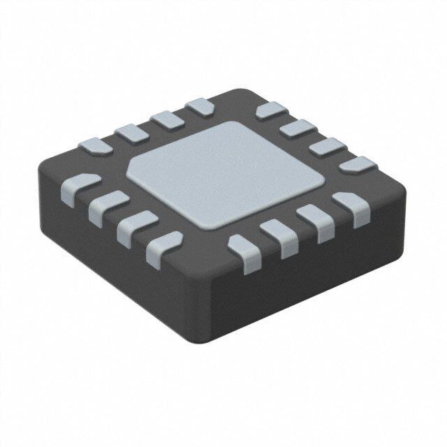
| 描述 | IC MODULATOR SIGE DIRECT 16-QFN |
| 产品分类 | RF 调制器 |
| LO频率 | 250MHz ~ 3.8GHz |
| 品牌 | Hittite Microwave Corporation |
| 数据手册 | 点击此处下载产品Datasheet |
| 产品图片 |  |
| P1dB | 2dBm |
| 产品型号 | HMC495LP3E |
| RF频率 | 250MHz ~ 3.8GHz |
| rohs | 无铅 / 符合限制有害物质指令(RoHS)规范要求 |
| 产品系列 | - |
| 其它名称 | 1127-1429 1127-1429-1 1127-1429-ND |
| 功能 | 调制器 |
| 包装 | 剪切带 (CT) |
| 封装/外壳 | 16-VQFN 裸露焊盘 |
| 本底噪声 | -158dBm/Hz |
| 标准包装 | 1 |
| 测试频率 | - |
| 特色产品 | http://www.digikey.cn/product-highlights/zh/direct-iq-modulators/52283 |
| 电压-电源 | 3 V ~ 3.6 V |
| 电流-电源 | 108mA |
| 输出功率 | -6dBm |
Datasheet
PDF Datasheet 数据手册内容提取
HMC495LP3 495LP3E / v02.0705 SiGe WIDEBAND DIRECT MODULATOR RFIC, 250 - 3800 MHz Typical Applications Features The HMC495LP3 / HMC495LP3E is suitable for Wideband RF Frequency Range various modulation systems: High Carrier Suppression: 38 dBc • UMTS, GSM or CDMA Basestations Very Low Noise Floor: -158 dBm/Hz E • Fixed Wireless or WLL Low LO Power: -6 to +6 dBm • ISM Transceivers, 900 & 2400 MHz Differential or Single Ended LO Input • GMSK, QPSK, QAM, SSB Modulators Single Low Current Supply: +3.3V@ 108 mA T Functional Diagram General Description 10 The HMC495LPE3 & HMC495LP3E are low noise Wideband Direct Quadrature Modulator RFICs which are ideal for digital modulation applications from 250 - T 3800 MHz including; Cellular/3G, Broadband Wireless M L Access & ISM circuits. Housed in a compact 3x3 mm S (LP3) SMT QFN package, the RFIC requires minimal - external components & provides a low cost alternative S O to more complicated double upconversion architec- R tures. The RF output port is single-ended and matched O to 50 Ohms with no external components. The LO re- T quires -6 to +6 dBm and can be driven in either dif- A S ferential or single-ended mode while the Baseband in- L U puts will support modulation inputs from DC - 250 MHz D typical. This device is optimized for a supply voltage of O +3.3V @ 108 mA and will provide stable performance B M over a +3V to +3.6V range. Electrical Specifi cations, See Test Conditions on following page herein. Parameter Min. Typ. Max. Min. Typ. Max. Min. Typ. Max. Min. Typ. Max. Units O Frequency Range, RF 450 - 960 1800 - 2200 2100 - 2700 3400 - 3800 MHz Output Power -7 -5 -8 -6 -9 -7 -11 -9 dBm Output P1dB 2 1 0 -2 dBm Output IP3 17 14 14 13 dBm Output Noise Floor -159 -158 -158 -157 dBm/Hz Carrier Suppression (uncalibrated) 38 38 35 34 dBc Sideband Suppression 34 31 30 28 dBc (uncalibrated) IM3 Suppression 59 50 50 56 dBc RF Port Return Loss 18 17 16 13 dB LO Port Return Loss 13 8 7 5 dB CDMA IS95 ACPR@ 880 MHz & 1960 MHz -72 -71.5 N/A N/A dBc Channel Power -15 -18.4 N/A N/A dBm W-CDMA 3GPP ACPR@ 1960 & 2140 MHz N/A -60 -59 N/A dBc Channel Power N/A -17.3 -14.4 N/A dBm Information furnishedF boy rA pnarloicg eD,e vdiceesl iivs eberlyie,v ead ntod b eto a cpculraatce ea nod rrdelieabrlse., Hpowleevaers, eno coFnotra pcrtic He,i tdteitleiv eMry,i carnodw toa vpela cCe oorrpdeorrsa: tAionanlo:g Devices, Inc., 10 - 10 rriegshptso nosf ibthiilritdy pisa artsiessu mtheadt2 mb0ya yAA rnealspluolght fDraoem vRi citeso su afsoedr. it,Ss p Cuescehif,i cenaoltrimo fnosrs asfnuoyb rjiendcfrt,i nt ogM ecmhAaenn gt0se 1 owf8 ipth2aot4uetn tnPso otihcr eoo.t hnNeore : 9OP7hnoe8n -Te2e: c57h80n1-o-33lo23g94y- 43W7 a0 yF0, a(cid:127)P x.OO:r .d 9Be7or 8xo n-92l1in05e60 ,a -Nt3 wo3rww7wo3o.adn, aMloAg .0c2o0m6 2-9106 lTicraednesem aisr kgsr aanndte dre gbiys teimrepdli ctraatdioenm oarr kost haerrew tihsee purnodpeerr tya noyf tphaetier nret sopOre pcratdivteeen otr wr ignOehrtnss .o-fl iAnnealo ga tD ewvicwesw. .hAipttpiltieca.ctioonm Support: Phone: 1-800-ANALOG-D
HMC495LP3 / 495LP3E v02.0705 SiGe WIDEBAND DIRECT MODULATOR RFIC, 250 - 3800 MHz Electrical Specifi cations, (continued) Parameter Conditions Min. Typ. Max. Units RF Output RF Frequency Range 0.25 3.8 GHz E RF Return Loss 16 dB LO Input LO Frequency Range 0.25 3.8 GHz LO Input Power With 68 Ohm shunt resistor on LO port. -6 0 +6 dBm T LO Port Return Loss With 68 Ohm shunt resistor on LO port. 7 dB Baseband Input Port 10 With 50Ω source & external 10 pF shunt cap to ground. Baseband Port Bandwidth DC 250 MHz Refer to HMC495LP3 Application Circuit. E This parameter can be varied in order to optimize Baseband Input DC Voltage (Vbbdc) 1.0 1.15 1.2 V the device performance over temperature and/or supply. T Baseband Input DC Bias Current (Ibbdc) Single-ended. 40 μA M Single-ended Baseband Input Capacitance De-embed to the lead of theL device. 0.5 pF DC Power Requirements See Test Conditions Below S Supply Voltage (Vcc1, Vcc2, Vb1, Vb2) 3 3.3 3.6 V - Supply Current (Icc1, Icc2, Ib1, Ib2) 108 mA S O R Test Conditions: Unless Otherwise Specifi ed, the Following Test Conditions Were Used O Parameter Condition T Temperature +25 °C A S Baseband Input Frequency 200 kHz L U Baseband Input DC Voltage (Vbbdc) 1.15V D Baseband Input AC Voltage (Peak to Peak Differential, I and Q) 800 mV O Baseband Input AC Voltage for OIP3 Measurement (Peak to Peak Differential, I and Q) 400 mV per tone @ 150 & 250 kHz B Frequency Offset for Output Noise Measurements 20 MHz M Supply & Bias Voltage (Vb1, Vb2, Vcc1, Vcc2) 3.3V LO Input Power 0 dBm LO Input Mode Single-Ended O Mounting Confi guration Refer to HMC495LP3 Application Schematic Herein Sideband & Carrier Feedthrough Uncalibrated Calibrated vs. Uncalibrated Test Results During the Uncalibrated Sideband and Carrier Suppression tests, care is taken to ensure that the I/Q signal paths from the Vector Signal Generator (VSG) to the Device Under Test (DUT) are equal. The “Uncalibrated, +25 °C” Sideband and Carrier Suppression plots were measured at room temperature, while the “Uncalibrated, over Temperature” Sideband and Carrier Suppression plots represent the worst case uncalibrated suppression levels measured at T= -40 °C, +25 °C, and +85 °C. The “Calibrated, + 25 °C” Sideband Suppression data was plotted after a manual adjustment of the I/Q amplitude balance and I/Q phase offset (skew) at +25 °C, and at each LO input power level. The +25 °C adjustment settings were held constant during tests over temperature. The “Calibrated, over Temperature” plots represent the worst case calibrated Sideband Suppression levels at T= -40 °C, +25 °C, and +85 °C. The “Calibrated, +25 °C” Carrier Suppression data was plotted after a manual adjustment of the Ip/In & Qp/Qn DC offsets at +25 °C, and at each LO input power level. The +25 °C adjustment settings were held constant during tests over temperature. The “Calibrated, over Temperature” plots represent the worst case Carrier Suppression levels measured at T= -40 °C, +25 °C, and +85 °C. Information furnishedF boy rA pnarloicg eD,e vdiceesl iivs eberlyie,v ead ntod b eto a cpculraatce ea nod rrdelieabrlse., Hpowleevaers, eno coFnotra pcrtic He,i tdteitleiv eMry,i carnodw toa vpela cCe oorrpdeorrsa: tAionanlo:g Devices, Inc., responsibility is assumed2 b0y AAnalplogh Dae vRiceos afodr it,s Cuseh, enolrm fors afnoy rindfr,in gMemAen t0s 1of8 p2at4en tPs ohr oothnere : 9O7ne8 -T2ec5h0n-o3lo3g4y 3W a yF, aPx.O: . 9B7o8x -9210560, -N3o3rw7o3od, MA 02062-9106 10 - 11 rights of third parties that may result from its use. Specifications subject to change without notice. No Phone: 781-329-4700 (cid:127) Order online at www.analog.com lTicraednesem aisr kgsr aanndte dre gbiys teimrepdli ctraatdioenm oarr kost haerrew tihsee purnodpeerr tya noyf tphaetier nret sopOre pcratdivteeen otr wr ignOehrtnss .o-fl iAnnealo ga tD ewvicwesw. .hAipttpiltieca.ctioonm Support: Phone: 1-800-ANALOG-D
HMC495LP3 / 495LP3E v02.0705 SiGe WIDEBAND DIRECT MODULATOR RFIC, 250 - 3800 MHz Output Noise Floor Wideband Performance vs. Frequency and P1dB vs. Frequency -120 5 10 WER (dBm), CARRIER SUPPR. (dBc)SUPPR. (dBc), 3rd HARMONIC (dBc) ---------544332211-05050505050 OSUIDTEPBUATN PDO SWUEPRPRESSION CARRIER SUPPRESSION ----------05443322115050505050 OUTPUT NOISE (dBm/Hz)----111165430000 T E ---011550OUTPUT P1dB (dBm) UT POBAND --6505 3rd HARMONIC --6505 -1700 400 800E1200S16E0T0-U2P0 0N0OI2S4E0 0FL2O8O00R3200 3600 400-020 TPDE 0 400 800 1200 1600 2000 2400 2800 3200 3600 4000 FREQUENCY (MHz) OUSI FREQUENCY (MHz) T M L S Output IP3 vs. Frequency Return Loss - 20 0 S 18 O R LO (Single-ended) 16 -5 RF O m) 14 dB) LAT PUT IP3 (dB 11802 S URN LOSS (--1150 U OUT 6 RET D 4 -20 O 2 B M 0 -25 0 400 800 1200 1600 2000 2400 2800 3200 3600 4000 0 400 800 1200 1600 2000 2400 2800 3200 3600 4000 FREQUENCY (MHz) FREQUENCY (MHz) O Information furnishedF boy rA pnarloicg eD,e vdiceesl iivs eberlyie,v ead ntod b eto a cpculraatce ea nod rrdelieabrlse., Hpowleevaers, eno coFnotra pcrtic He,i tdteitleiv eMry,i carnodw toa vpela cCe oorrpdeorrsa: tAionanlo:g Devices, Inc., 10 - 12 rriegshptso nosf ibthiilritdy pisa artsiessu mtheadt2 mb0ya yAA rnealspluolght fDraoem vRi citeso su afsoedr. it,Ss p Cuescehif,i cenaoltrimo fnosrs asfnuoyb rjiendcfrt,i nt ogM ecmhAaenn gt0se 1 owf8 ipth2aot4uetn tnPso otihcr eoo.t hnNeore : 9OP7hnoe8n -Te2e: c57h80n1-o-33lo23g94y- 43W7 a0 yF0, a(cid:127)P x.OO:r .d 9Be7or 8xo n-92l1in05e60 ,a -Nt3 wo3rww7wo3o.adn, aMloAg .0c2o0m6 2-9106 lTicraednesem aisr kgsr aanndte dre gbiys teimrepdli ctraatdioenm oarr kost haerrew tihsee purnodpeerr tya noyf tphaetier nret sopOre pcratdivteeen otr wr ignOehrtnss .o-fl iAnnealo ga tD ewvicwesw. .hAipttpiltieca.ctioonm Support: Phone: 1-800-ANALOG-D
HMC495LP3 / 495LP3E v02.0705 SiGe WIDEBAND DIRECT MODULATOR RFIC, 250 - 3800 MHz Output IP3 & Output Power vs. Output IP3 & Output Power vs. LO Power Over Temperature@ 830 MHz LO Power Over Supply@ 830 MHz 20 -3 20 -3 15 -4 15 -4 OU E OU m) 10 -5T m) 10 -5T T IP3 (dB 5 -6PUT POW T IP3 (dB 5 -6PUT POW U E U E OUTP 0 ++-428055 CCC -7R (dB OUTP 0 TVVVcccccc=== 333...036 VVVooollltttsss -7R (dB m m -5 -8) -5 -8) 10 -10 -9 -10 E -9 -6 -5 -4 -3 -2 -1 0 1 2 3 4 5 6 -6 -5 -4 -3 -2 -1 0 1 2 3 4 5 6 LO POWER (dBm) LO POWER (dBm) T M L Output Noise vs. LO Power Output Noise vs. LO Power S Over Temperature@ 830 MHz Over Supply@ 830 MHz - -140 -140 S O R z) +25 C z) Vcc= 3.0 Volts m/H-145 + -8450 CC m/H-145 VVcccc== 33..36 VVoollttss O B B d d T OISE (-150 S OISE (-150 A N N L UT UT U P P UT-155 UT-155 D O O O B -160 -160 M -6 -5 -4 -3 -2 -1 0 1 2 3 4 5 6 -6 -5 -4 -3 -2 -1 0 1 2 3 4 5 6 LO POWER (dBm) LO POWER (dBm) O Sideband Suppression* Carrier Suppression* vs. LO Power@ 830 MHz vs. LO Power@ 830 MHz -20 -20 BAND SUPPRESSION (dBc)---543000 UCNALCIABLRIABTREADT,E +D2,5 +C25C RIER SUPPRESSION (dBc)---543000 UCUCNANALLCCIIAABBLLRRIIAABBTTRREEAADDTT,,EE +ODD2V,,5 OEC+RV2 5ETCRE MTEPMP E UNCALIBRATED, OVER TEMP R D CALIBRATED, OVER TEMP A SI C -60 -60 -6 -5 -4 -3 -2 -1 0 1 2 3 4 5 6 -6 -5 -4 -3 -2 -1 0 1 2 3 4 5 6 LO POWER (dBm) LO POWER (dBm) * See note titled “Calibrated vs. Uncalibrated test results” herein. Information furnishedF boy rA pnarloicg eD,e vdiceesl iivs eberlyie,v ead ntod b eto a cpculraatce ea nod rrdelieabrlse., Hpowleevaers, eno coFnotra pcrtic He,i tdteitleiv eMry,i carnodw toa vpela cCe oorrpdeorrsa: tAionanlo:g Devices, Inc., responsibility is assumed2 b0y AAnalplogh Dae vRiceos afodr it,s Cuseh, enolrm fors afnoy rindfr,in gMemAen t0s 1of8 p2at4en tPs ohr oothnere : 9O7ne8 -T2ec5h0n-o3lo3g4y 3W a yF, aPx.O: . 9B7o8x -9210560, -N3o3rw7o3od, MA 02062-9106 10 - 13 rights of third parties that may result from its use. Specifications subject to change without notice. No Phone: 781-329-4700 (cid:127) Order online at www.analog.com lTicraednesem aisr kgsr aanndte dre gbiys teimrepdli ctraatdioenm oarr kost haerrew tihsee purnodpeerr tya noyf tphaetier nret sopOre pcratdivteeen otr wr ignOehrtnss .o-fl iAnnealo ga tD ewvicwesw. .hAipttpiltieca.ctioonm Support: Phone: 1-800-ANALOG-D
HMC495LP3 / 495LP3E v02.0705 SiGe WIDEBAND DIRECT MODULATOR RFIC, 250 - 3800 MHz Output IP3 & Output Power vs. Output IP3 & Output Power vs. LO Power Over Temperature@ 1900 MHz LO Power Over Supply@ 1900 MHz 20 -3 20 -3 15 -4 15 -4 OU E OU m) 10 -5 T m) 10 -5T T IP3 (dB 5 ++-428055 CCC -6 PUT POW T IP3 (dB 5 VVVcccccc=== 333...036 VVVooollltttsss -6PUT POW U E U E UTP 0 -7 R (d UTP 0 T -7R (d O B O B m m -5 -8 ) -5 -8) 10 -10 -9 -10 E -9 -6 -5 -4 -3 -2 -1 0 1 2 3 4 5 6 -6 -5 -4 -3 -2 -1 0 1 2 3 4 5 6 LO POWER (dBm) LO POWER (dBm) T M L Output Noise vs. LO Power Output Noise vs. LO Power S Over Temperature@ 1900 MHz Over Supply@ 1900 MHz - -140 -140 S O R O m/Hz)-145 ++ -284550 CCC m/Hz)-145 VVVcccccc=== 333...036 VVVooollltttsss B B AT OISE (d-150 S OISE (d-150 L N N U UT UT P P D UT-155 UT-155 O O O B M -160 -160 -6 -5 -4 -3 -2 -1 0 1 2 3 4 5 6 -6 -5 -4 -3 -2 -1 0 1 2 3 4 5 6 LO POWER (dBm) LO POWER (dBm) O Sideband Suppression* Carrier Suppression* vs. LO Power@ 1900 MHz vs. LO Power@ 1900 MHz -20 -20 BAND SUPPRESSION (dBc)---543000 UCNALCIABLRIABTREADT,E D+2, 5+ 2C5 C RIER SUPPRESSION (dBc)---543000 UCUCNANALLCCIIAABBLLRRIIAABBTTRREEAADDTT,,EE ODD+V2,, 5+OE 2RVC5 ET CRE MTEPMP E UNCALIBRATED, OVER TEMP R D CALIBRATED, OVER TEMP A SI C -60 -60 -6 -5 -4 -3 -2 -1 0 1 2 3 4 5 6 -6 -5 -4 -3 -2 -1 0 1 2 3 4 5 6 LO POWER (dBm) LO POWER (dBm) * See note titled “Calibrated vs. Uncalibrated test results” herein. Information furnishedF boy rA pnarloicg eD,e vdiceesl iivs eberlyie,v ead ntod b eto a cpculraatce ea nod rrdelieabrlse., Hpowleevaers, eno coFnotra pcrtic He,i tdteitleiv eMry,i carnodw toa vpela cCe oorrpdeorrsa: tAionanlo:g Devices, Inc., 10 - 14 rriegshptso nosf ibthiilritdy pisa artsiessu mtheadt2 mb0ya yAA rnealspluolght fDraoem vRi citeso su afsoedr. it,Ss p Cuescehif,i cenaoltrimo fnosrs asfnuoyb rjiendcfrt,i nt ogM ecmhAaenn gt0se 1 owf8 ipth2aot4uetn tnPso otihcr eoo.t hnNeore : 9OP7hnoe8n -Te2e: c57h80n1-o-33lo23g94y- 43W7 a0 yF0, a(cid:127)P x.OO:r .d 9Be7or 8xo n-92l1in05e60 ,a -Nt3 wo3rww7wo3o.adn, aMloAg .0c2o0m6 2-9106 lTicraednesem aisr kgsr aanndte dre gbiys teimrepdli ctraatdioenm oarr kost haerrew tihsee purnodpeerr tya noyf tphaetier nret sopOre pcratdivteeen otr wr ignOehrtnss .o-fl iAnnealo ga tD ewvicwesw. .hAipttpiltieca.ctioonm Support: Phone: 1-800-ANALOG-D
HMC495LP3 / 495LP3E v02.0705 SiGe WIDEBAND DIRECT MODULATOR RFIC, 250 - 3800 MHz Output IP3 & Output Power vs. Output IP3 & Output Power vs. LO Power Over Temperature@ 2100 MHz LO Power Over Supply@ 2100 MHz 20 -3 20 -3 15 -4 15 -4 OU E OU m) 10 -5T m) 10 -5T T IP3 (dB 5 -6PUT POW T IP3 (dB 5 VVVcccccc=== 333...036 VVVooollltttsss -6PUT POW U E U E UTP 0 -7R (d UTP 0 T -7R (d O B O B m m -5 ++2855 CC -8) -5 -8) 10 -40 C -10 -9 -10 E -9 -6 -5 -4 -3 -2 -1 0 1 2 3 4 5 6 -6 -5 -4 -3 -2 -1 0 1 2 3 4 5 6 LO POWER (dBm) LO POWER (dBm) T M L Output Noise vs. LO Power Output Noise vs. LO Power S Over Temperature@ 2100 MHz Over Supply@ 2100 MHz - -140 -140 S O R z) +25 C z) Vcc= 3.0 Volts m/H-145 + -8450 CC m/H-145 VVcccc== 33..36 VVoollttss O B B d d T OISE (-150 S OISE (-150 A N N L UT UT U P P UT-155 UT-155 D O O O B -160 -160 M -6 -5 -4 -3 -2 -1 0 1 2 3 4 5 6 -6 -5 -4 -3 -2 -1 0 1 2 3 4 5 6 LO POWER (dBm) LO POWER (dBm) O Sideband Suppression* Carrier Suppression* vs. LO Power@ 2100 MHz vs. LO Power@ 2100 MHz -20 -20 EBAND SUPPRESSION (dBc)---543000 UCUNANLCCIAABLLRIIABBTRREAADTT,EE DD+2,, 5 O+CV25ECR TEMP RRIER SUPPRESSION (dBc)---543000 UCUCNANALLCCIIAABBLLRRIIAABBTTRREEAADDTT,,EE +ODD2V,,5 OEC+RV2 5ETCRE MTEPMP D CALIBRATED, OVER TEMP A SI C -60 -60 -6 -5 -4 -3 -2 -1 0 1 2 3 4 5 6 -6 -5 -4 -3 -2 -1 0 1 2 3 4 5 6 LO POWER (dBm) LO POWER (dBm) * See note titled “Calibrated vs. Uncalibrated test results” herein. Information furnishedF boy rA pnarloicg eD,e vdiceesl iivs eberlyie,v ead ntod b eto a cpculraatce ea nod rrdelieabrlse., Hpowleevaers, eno coFnotra pcrtic He,i tdteitleiv eMry,i carnodw toa vpela cCe oorrpdeorrsa: tAionanlo:g Devices, Inc., responsibility is assumed2 b0y AAnalplogh Dae vRiceos afodr it,s Cuseh, enolrm fors afnoy rindfr,in gMemAen t0s 1of8 p2at4en tPs ohr oothnere : 9O7ne8 -T2ec5h0n-o3lo3g4y 3W a yF, aPx.O: . 9B7o8x -9210560, -N3o3rw7o3od, MA 02062-9106 10 - 15 rights of third parties that may result from its use. Specifications subject to change without notice. No Phone: 781-329-4700 (cid:127) Order online at www.analog.com lTicraednesem aisr kgsr aanndte dre gbiys teimrepdli ctraatdioenm oarr kost haerrew tihsee purnodpeerr tya noyf tphaetier nret sopOre pcratdivteeen otr wr ignOehrtnss .o-fl iAnnealo ga tD ewvicwesw. .hAipttpiltieca.ctioonm Support: Phone: 1-800-ANALOG-D
HMC495LP3 / 495LP3E v02.0705 SiGe WIDEBAND DIRECT MODULATOR RFIC, 250 - 3800 MHz Cellular CDMA @ 880 MHz PCS CDMA @ 1960 MHz ACPR @ 885 kHz, Vcc= 3.3V, Vdc= 1.15V ACPR @ 885 kHz, Vcc= 3.3V, Vdc= 1.15V -20 -20 -30 -30 -40 -40 E m)-50 m)-50 B B R (d-60 R (d-60 E CP = -15dBm CP = -15dBm E W ACPR = -72.3dBc ACPR = -72dBc W O-70 O-70 P P CP = -18.42dBm TCP = -18.42dBm -80 -80 ACPR = -71.5dBc ACPR = -71.5dBc 10 -90 -90 -100 -100 E 879 879.3 879.5 879.8 880 880.3 880.5 880.8 881 1959 1959.25 1959.5 1959.75 1960 1960.25 1960.5 1960.75 1961 FREQUENCY (MHz) FREQUENCY (MHz) T M L W-CDMA @ 1960 MHz W-CDMA @ 2140 MHz S ACPR @ 3.84 MHz, Vcc= 3.3V, Vdc= 1.15V ACPR @ 3.84 MHz, Vcc= 3.3V, Vdc= 1.15V - -20 -20 S O -30 -30 R CP = -17.3dBm CP = -17.3dBm CP = -14.4Bm CP = -14.4dBm ACPR = -59.7dBc ACPR = -59.8dBc ACPR = -59.2dBc ACPR = -59.8dBc O -40 -40 T Bm)-50 Bm)-50 d d A R (-60 R (-60 E S E L W W U PO-70 PO-70 D -80 -80 O -90 -90 B M -100 -100 1955 1956 1957 1958 1959 1960 1961 1962 1963 1964 1965 2135 2136 2137 2138 2139 2140 2141 2142 2143 2144 2145 FREQUENCY (MHz) FREQUENCY (MHz) O Note 1: W-CDMA (Modulation Set-up for ACPR Mode); The Baseband I and Q input signals were generated using “Test Model 1 with 64 channels” settings in the Agilent E3844C. Note 2: CDMA (Modulation Set-up for ACPR Mode); The Baseband I and Q input signals were generated using the “9 channels forward” settings in the Agilent E3844C (pilot, paging, sync and 6 traffic channels). Information furnishedF boy rA pnarloicg eD,e vdiceesl iivs eberlyie,v ead ntod b eto a cpculraatce ea nod rrdelieabrlse., Hpowleevaers, eno coFnotra pcrtic He,i tdteitleiv eMry,i carnodw toa vpela cCe oorrpdeorrsa: tAionanlo:g Devices, Inc., 10 - 16 rriegshptso nosf ibthiilritdy pisa artsiessu mtheadt2 mb0ya yAA rnealspluolght fDraoem vRi citeso su afsoedr. it,Ss p Cuescehif,i cenaoltrimo fnosrs asfnuoyb rjiendcfrt,i nt ogM ecmhAaenn gt0se 1 owf8 ipth2aot4uetn tnPso otihcr eoo.t hnNeore : 9OP7hnoe8n -Te2e: c57h80n1-o-33lo23g94y- 43W7 a0 yF0, a(cid:127)P x.OO:r .d 9Be7or 8xo n-92l1in05e60 ,a -Nt3 wo3rww7wo3o.adn, aMloAg .0c2o0m6 2-9106 lTicraednesem aisr kgsr aanndte dre gbiys teimrepdli ctraatdioenm oarr kost haerrew tihsee purnodpeerr tya noyf tphaetier nret sopOre pcratdivteeen otr wr ignOehrtnss .o-fl iAnnealo ga tD ewvicwesw. .hAipttpiltieca.ctioonm Support: Phone: 1-800-ANALOG-D
HMC495LP3 / 495LP3E v02.0705 SiGe WIDEBAND DIRECT MODULATOR RFIC, 250 - 3800 MHz Absolute Maximum Ratings Vcc1, Vcc2, VB1, VB2 -0.5 to +6V ELECTROSTATIC SENSITIVE DEVICE LO Input Power +10 dBm Max. OBSERVE HANDLING PRECAUTIONS Baseband Input Voltage -0.5 to +1.8V E (Reference to GND) Channel Temperature 150 °C Continuous Pdiss (T = 85°C) 2.83 Watts (Derate 43.5 mW/°C above 85°C) T Thermal Resistance (R ) th 23 °C/Watt (junction to lead) 10 Storage Temperature -40 to +150 °C Operating Temperature -40 to +85 °C E Outline Drawing T M L S - S O R O T A S L U D O B M O NOTES: 1. LEADFRAME MATERIAL: COPPER ALLOY 2. DIMENSIONS ARE IN INCHES [MILLIMETERS]. 3. LEAD SPACING TOLERANCE IS NON-CUMULATIVE 4. PAD BURR LENGTH SHALL BE 0.15mm MAXIMUM. PAD BURR HEIGHT SHALL BE 0.05mm MAXIMUM. 5. PACKAGE WARP SHALL NOT EXCEED 0.05mm. 6. ALL GROUND LEADS AND GROUND PADDLE MUST BE SOLDERED TO PCB RF GROUND. 7. REFER TO HITTITE APPLICATION NOTE FOR SUGGESTED PCB LAND PATTERN. Package Information Part Number Package Body Material Lead Finish MSL Rating Package Marking [3] HMC495LP3 Low Stress Injection Molded Plastic Sn/Pb Solder MSL1 [1] 495 XXXX HMC495LP3E RoHS-compliant Low Stress Injection Molded Plastic 100% matte Sn MSL1 [2] 495 XXXX [1] Max peak refl ow temperature of 235 °C [2] Max peak refl ow temperature of 260 °C [3] 4-Digit lot number XXXX Information furnishedF boy rA pnarloicg eD,e vdiceesl iivs eberlyie,v ead ntod b eto a cpculraatce ea nod rrdelieabrlse., Hpowleevaers, eno coFnotra pcrtic He,i tdteitleiv eMry,i carnodw toa vpela cCe oorrpdeorrsa: tAionanlo:g Devices, Inc., responsibility is assumed2 b0y AAnalplogh Dae vRiceos afodr it,s Cuseh, enolrm fors afnoy rindfr,in gMemAen t0s 1of8 p2at4en tPs ohr oothnere : 9O7ne8 -T2ec5h0n-o3lo3g4y 3W a yF, aPx.O: . 9B7o8x -9210560, -N3o3rw7o3od, MA 02062-9106 10 - 17 rights of third parties that may result from its use. Specifications subject to change without notice. No Phone: 781-329-4700 (cid:127) Order online at www.analog.com lTicraednesem aisr kgsr aanndte dre gbiys teimrepdli ctraatdioenm oarr kost haerrew tihsee purnodpeerr tya noyf tphaetier nret sopOre pcratdivteeen otr wr ignOehrtnss .o-fl iAnnealo ga tD ewvicwesw. .hAipttpiltieca.ctioonm Support: Phone: 1-800-ANALOG-D
HMC495LP3 / 495LP3E v02.0705 SiGe WIDEBAND DIRECT MODULATOR RFIC, 250 - 3800 MHz Pin Descriptions Pin Number Function Description Interface Schematic These pins and the ground paddle must be connected to a 1, 4, 9, 12 GND high quality RF/DC ground. E Differential LO input ports. This device may be driven in either differential or single ended mode. In single ended mode, one port should be driven by the LO source while the other port may be terminated with a 50Ω resistor to 2, 3 LOP, LON T ground. An external shunt 68Ω resistor is used to improve VSWR, while an external 100 pF capacitor is required 10 to prevent DC supply voltage from appearing on the customer’s PC board. E Bias Voltage for the LO stage. This voltage will affect the T Sideband Suppression, the Output Noise Floor and the M 5 VB2 Power Consumption. The ideal voltage range for this port L is between +2.7 Vdc and +3.0 Vdc. The nominal current for S this port is 5.3 mA. - S O R Differential Quadrature baseband input. These are high impedance ports. The nominal recommended bias O voltage is between 1.0 - 1.15V. The nominal recommended T baseband input voltage is 800 mV peak to peak differential. A By adjusting the DC bias voltage on ports Qn & Qp, the Carrier SuppSression of the device can be optimized for a L 6, 7 Qn, Qp specifi c frequency band and LO power level. The typical U offset voltage for optimization is less than 5 mV. D The amplitude and phase difference between the I and Q O inputs can be adjusted in order to optimize the Sideband B Suppression for a specifi c frequency band M and LO power level. Bias Voltage for the output stage. This voltage should be O 8 VB1 connected to the Vcc supply. Nominal supply voltage is 3.3 Vdc. The nominal current for this port is 2.4 mA. 10 N/C No connect. RF Output port. This port is matched to 50Ω. A series capacitor should be connected to this port in order to 11 RFP prevent the DC supply voltage from appearing on the customer’s PC board. Information furnishedF boy rA pnarloicg eD,e vdiceesl iivs eberlyie,v ead ntod b eto a cpculraatce ea nod rrdelieabrlse., Hpowleevaers, eno coFnotra pcrtic He,i tdteitleiv eMry,i carnodw toa vpela cCe oorrpdeorrsa: tAionanlo:g Devices, Inc., 10 - 18 rriegshptso nosf ibthiilritdy pisa artsiessu mtheadt2 mb0ya yAA rnealspluolght fDraoem vRi citeso su afsoedr. it,Ss p Cuescehif,i cenaoltrimo fnosrs asfnuoyb rjiendcfrt,i nt ogM ecmhAaenn gt0se 1 owf8 ipth2aot4uetn tnPso otihcr eoo.t hnNeore : 9OP7hnoe8n -Te2e: c57h80n1-o-33lo23g94y- 43W7 a0 yF0, a(cid:127)P x.OO:r .d 9Be7or 8xo n-92l1in05e60 ,a -Nt3 wo3rww7wo3o.adn, aMloAg .0c2o0m6 2-9106 lTicraednesem aisr kgsr aanndte dre gbiys teimrepdli ctraatdioenm oarr kost haerrew tihsee purnodpeerr tya noyf tphaetier nret sopOre pcratdivteeen otr wr ignOehrtnss .o-fl iAnnealo ga tD ewvicwesw. .hAipttpiltieca.ctioonm Support: Phone: 1-800-ANALOG-D
HMC495LP3 / 495LP3E v02.0705 SiGe WIDEBAND DIRECT MODULATOR RFIC, 250 - 3800 MHz Pin Descriptions (continued) Pin Number Function Description Interface Schematic Supply voltage for the mixer and output stages. 13 Vcc1 Set to 3.3V for nominal operation. The nominal E current for this port is 37 mA. Differential In-Phase baseband input. These are high impedance ports. The nominal recommended bias voltage T is between 1.0 - 1.15V.The nominal recommened baseband input voltage is 800 mV peak to peak differential. By adjusting the DC bias voltage on ports In & Ip, the Carrier 10 Suppression of the device can be optimized for a specifi c 14, 15 Ip, In frequency band and LO power level. The typical offset E voltage for optimization is less than 5 mV. The amplitude and phase difference between the I and Q inputs can be adjusted in order to optimize the Sideband T Suppression for a specifi c frequency band and LO power level. L M S 16 Vcc2 Supply voltage for the LO stage. Set to 3.3V for nominal - operation. The nominal current for this port is 64 mA. S O R O T A S L U D O B M O Information furnishedF boy rA pnarloicg eD,e vdiceesl iivs eberlyie,v ead ntod b eto a cpculraatce ea nod rrdelieabrlse., Hpowleevaers, eno coFnotra pcrtic He,i tdteitleiv eMry,i carnodw toa vpela cCe oorrpdeorrsa: tAionanlo:g Devices, Inc., responsibility is assumed2 b0y AAnalplogh Dae vRiceos afodr it,s Cuseh, enolrm fors afnoy rindfr,in gMemAen t0s 1of8 p2at4en tPs ohr oothnere : 9O7ne8 -T2ec5h0n-o3lo3g4y 3W a yF, aPx.O: . 9B7o8x -9210560, -N3o3rw7o3od, MA 02062-9106 10 - 19 rights of third parties that may result from its use. Specifications subject to change without notice. No Phone: 781-329-4700 (cid:127) Order online at www.analog.com lTicraednesem aisr kgsr aanndte dre gbiys teimrepdli ctraatdioenm oarr kost haerrew tihsee purnodpeerr tya noyf tphaetier nret sopOre pcratdivteeen otr wr ignOehrtnss .o-fl iAnnealo ga tD ewvicwesw. .hAipttpiltieca.ctioonm Support: Phone: 1-800-ANALOG-D
HMC495LP3 / 495LP3E v02.0705 SiGe WIDEBAND DIRECT MODULATOR RFIC, 250 - 3800 MHz Evaluation PCB E T 10 E T M L S - S O R O T A S L U D O B M O List of Materials for Evaluation PCB 107413 [1] Item Description The circuit board used in the fi nal application should J1 - J8 PCB Mount SMA Connector use RF circuit design techniques. Signal lines J9 - J12 DC Molex Connector should have 50 ohm impedance while the package C1, C2, C7 100 pF Chip Capacitor, 0402 Pkg. ground leads and exposed paddle should be con- C3, C6, C8, C11 1000 pF Chip Capacitor, 0402 Pkg. nected directly to the ground plane similar to that C4, C5, C9, C10 10 pF Chip Capacitor, 0402 Pkg. shown. A sufficient number of via holes should be C12 - C15 4.7 uF, Case A, Tantulum used to connect the top and bottom ground planes. R1, R2 68 Ohms, 0402 Pkg. The evaluation circuit board shown is available from R3 62 Ohms, 0402 Pkg. Hittite upon request. U1 HMC495LP3 / HMC495LP3E Modulator PCB [2] 107309 Eval Board [1] Reference this number when ordering complete evaulation PCB [2] Circuit Board Material: Rogers 4350 Information furnishedF boy rA pnarloicg eD,e vdiceesl iivs eberlyie,v ead ntod b eto a cpculraatce ea nod rrdelieabrlse., Hpowleevaers, eno coFnotra pcrtic He,i tdteitleiv eMry,i carnodw toa vpela cCe oorrpdeorrsa: tAionanlo:g Devices, Inc., 10 - 20 rriegshptso nosf ibthiilritdy pisa artsiessu mtheadt2 mb0ya yAA rnealspluolght fDraoem vRi citeso su afsoedr. it,Ss p Cuescehif,i cenaoltrimo fnosrs asfnuoyb rjiendcfrt,i nt ogM ecmhAaenn gt0se 1 owf8 ipth2aot4uetn tnPso otihcr eoo.t hnNeore : 9OP7hnoe8n -Te2e: c57h80n1-o-33lo23g94y- 43W7 a0 yF0, a(cid:127)P x.OO:r .d 9Be7or 8xo n-92l1in05e60 ,a -Nt3 wo3rww7wo3o.adn, aMloAg .0c2o0m6 2-9106 lTicraednesem aisr kgsr aanndte dre gbiys teimrepdli ctraatdioenm oarr kost haerrew tihsee purnodpeerr tya noyf tphaetier nret sopOre pcratdivteeen otr wr ignOehrtnss .o-fl iAnnealo ga tD ewvicwesw. .hAipttpiltieca.ctioonm Support: Phone: 1-800-ANALOG-D
HMC495LP3 / 495LP3E v02.0705 SiGe WIDEBAND DIRECT MODULATOR RFIC, 250 - 3800 MHz Application & Evaluation PCB Schematic E T 10 E T M L S - S O R O T A S L U D Note: O Baseband input frequency range is dBependent on value of C4, C5, C9 and C10. The value of 10 pF was chosen to give a typical response of DC - 250 MHz. Input frequency range can be extended up to 1 GHz with possible degradation of LO leakage and M broadband noise fl oor response by decreasing the value of C4, C5, C9 & C10. CharacterizatioOn Set-up Information furnishedF boy rA pnarloicg eD,e vdiceesl iivs eberlyie,v ead ntod b eto a cpculraatce ea nod rrdelieabrlse., Hpowleevaers, eno coFnotra pcrtic He,i tdteitleiv eMry,i carnodw toa vpela cCe oorrpdeorrsa: tAionanlo:g Devices, Inc., responsibility is assumed2 b0y AAnalplogh Dae vRiceos afodr it,s Cuseh, enolrm fors afnoy rindfr,in gMemAen t0s 1of8 p2at4en tPs ohr oothnere : 9O7ne8 -T2ec5h0n-o3lo3g4y 3W a yF, aPx.O: . 9B7o8x -9210560, -N3o3rw7o3od, MA 02062-9106 10 - 21 rights of third parties that may result from its use. Specifications subject to change without notice. No Phone: 781-329-4700 (cid:127) Order online at www.analog.com lTicraednesem aisr kgsr aanndte dre gbiys teimrepdli ctraatdioenm oarr kost haerrew tihsee purnodpeerr tya noyf tphaetier nret sopOre pcratdivteeen otr wr ignOehrtnss .o-fl iAnnealo ga tD ewvicwesw. .hAipttpiltieca.ctioonm Support: Phone: 1-800-ANALOG-D