首页 > HMC481MP86E > 详情
 Datasheet下载
- 型号: HMC481MP86E
- 制造商: Hittite
- 库位|库存: xxxx|xxxx
- 要求:
| 数量阶梯 | 香港交货 | 国内含税 |
| +xxxx | $xxxx | ¥xxxx |
查看当月历史价格
查看今年历史价格
产品参数
| 参数 | 数值 |
| 产品目录 | 射频/IF 和 RFID |
| 描述 | IC MMIC AMP HBT 5GHZ MICRO-P |
| 产品分类 | RF 放大器 |
| 品牌 | Hittite Microwave Corporation |
| 数据手册 | 点击此处下载产品Datasheet |
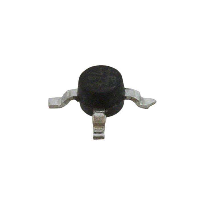
| 产品图片 |  |
| P1dB | 20dBm |
| 产品型号 | HMC481MP86E |
| RF类型 | 通用 |
| rohs | 无铅 / 符合限制有害物质指令(RoHS)规范要求 |
| 产品系列 | - |
| 供应商器件封装 | SOT-86 |
| 其它名称 | 1127-1419 |
| 包装 | 散装 |
| 噪声系数 | 3.5dB ~ 4.5dB |
| 增益 | 20dB |
| 封装/外壳 | SOT-86 |
| 标准包装 | 100 |
| 测试频率 | - |
| 电压-电源 | 6 V ~ 12 V |
| 电流-电源 | 74mA |
| 频率 | 0Hz ~ 5GHz |
Datasheet
PDF Datasheet 数据手册内容提取
HMC481MP86 481MP86E / v03.0810 SiGe HBT GAIN BLOCK MMIC AMPLIFIER, DC - 5 GHz Typical Applications Features 8 The HMC481MP86 / HMC481MP86E is an ideal RF/ P1dB Output Power: +20 dBm IF gain block & LO or PA driver for: Gain: 20 dB • Cellular / PCS / 3G Output IP3: +33 dBm T • Fixed Wireless & WLAN Cascadable 50 Ohm I/Os M • CATV, Cable Modem & DBS Single Supply: +6V to +12V S • Microwave Radio& Test Equipment Included in the HMC-DK001 Designer’s Kit - K Functional Diagram General Description C The HMC481MP86 & HMC481MP86E are SiGe O Heterojunction Bipolar Transistor (HBT) Gain Block L B MMIC SMT amplifi ers covering DC to 5 GHz. This Micro-P packaged amplifi er can be used as a cas- N cadable 50 Ohm RF/IF gain stage as well as a LO I A or PA driver with up to +21 dBm output power. The G HMC481MP86(E) offers 20 dB of gain with a +33 dBm & output IP3 at 850 MHz while requiring only 74 mA from a single positive supply. The Darlington feedback R pair used results in reduced sensitivity to normal E process variations and excellent gain stability over V I temperature while requiring a minimal number of R external bias components. D Electrical Specifi cations, Vs= 8.0 V, Rbias= 39 Ohm, T = +25° C - A S Parameter Min. Typ. Max. Units R DC - 1.0 GHz 18.5 20.0 dB E 1.0 - 2.0 GHz 15.5 17.0 dB Gain 2.0 - 3.0 GHz 12.5 14.0 dB I F 3.0 - 4.0 GHz 10.5 12.0 dB I 4.0 - 5.0 GHz 9.0 10.5 dB L Gain Variation Over Temperature DC - 5 GHz 0.008 0.012 dB/ °C P DC - 1.0 GHz 13 dB M Input Return Loss 1.0 - 5.0 GHz 17 dB A DC - 1.0 GHz 20 dB Output Return Loss 1.0 - 4.0 GHz 25 dB 4.0 - 5.0 GHz 15 dB Reverse Isolation DC - 5 GHz 18 dB 0.5 - 1.0 GHz 16 20 dBm 1.0 - 2.0 GHz 15 18 dBm Output Power for 1 dB Compression (P1dB) 2.0 - 3.0 GHz 14 17 dBm 3.0 - 4.0 GHz 12 15 dBm 4.0 - 5.0 GHz 9 12 dBm 0.5 - 2.0 GHz 33 dBm Output Third Order Intercept (IP3) 2.0 - 3.0 GHz 31 dBm (Pout= 0 dBm per tone, 1 MHz spacing) 3.0 - 4.0 GHz 29 dBm 4.0 - 5.0 GHz 26 dBm DC - 2.0 GHz 3.5 dB Noise Figure 2.0 - 4.0 GHz 4.0 dB 4.0 - 5.0 GHz 4.5 dB Supply Current (Icq) 74 85 mA Note: Data taken with broadband bias tee on device output. InforFmaotiro np fruircniseh,e dd beyl iAvnealroyg Daenvidce st ois pbelaliecveed otor dbee arcsc:u rHateit taintde reMliaibcler. oHwowaevveer, Cnoo rpFoorr aptriiocen,, d2e0liv Aerlyp, haand R too apdla,c Ce horedlemrss: fAonrdal,o gM DAe v0ic1e8s2, 4Inc., responsibility is assumed by Analog Devices for its use, nor for any infringements of patents or other One Technology Way, P.O. Box 9106, Norwood, MA 02062-9106 8 - 1 rliicgehntss eo fi sth girrda nptaerdti ebsy t himatp mlicaaPyt iorhenso uonlrt ofertoh:m e9r wit7sis 8ues -eu2.n dS5epr0e ca-inf3iyc 3aptia4otne3sn ts ou rb jpeFacttae tnoxt c:r hig9ahn7tgs 8eo wf- 2Aithn5oau0lot g-n 3oDti3ecve7i.c 3eNso . POhrodnee:r 7 O81n-3-2li9n-e4 7a0t0 w(cid:127) Owrwde.hr oitntliitnee. cato wmww.analog.com Trademarks and registered trademarks arAe tphep plriocpearttyi oof nth eSir urespppecotivret :o wPnehrso.ne: 978-250-3A3p4p3li c aotrio na Spuppsp@orht: iPtthitoen.ec: o1-m800-ANALOG-D
HMC481MP86 / 481MP86E v03.0810 SiGe HBT GAIN BLOCK MMIC AMPLIFIER, DC - 5 GHz Broadband Gain & Return Loss Gain vs. Temperature 8 25 24 15 20 B) 5 16 d S21 T NSE ( -5 SS1212 N (dB) 12 M RESPO -15 GAI 8 ++2855 CC S -40 C - -25 4 K C -35 0 O 0 1 2 3 4 5 6 7 8 0 1 2 3 4 5 6 FREQUENCY (GHz) FREQUENCY (GHz) L B N I Input Return Loss vs. Temperature Output Return Loss vs. Temperature A G 0 0 & -5 -5 +25 C +25 C +85 C dB) -10 +-4805 CC dB) -10 -40 C R S ( S ( E S S -15 O O V L -15 L RN RN -20 RI U U T -20 T RE RE -25 D -25 -30 - S -30 -35 R 0 1 2 3 4 5 6 0 1 2 3 4 5 6 FREQUENCY (GHz) FREQUENCY (GHz) E I F I L Reverse Isolation vs. Temperature Noise Figure vs. Temperature P M 0 10 A ATION (dB) -1-05 ++-428055 CCC RE (dB) 68 ++-428055 CCC L U O -15 G E IS E FI 4 VERS -20 NOIS RE -25 2 -30 0 0 1 2 3 4 5 6 0 1 2 3 4 5 6 FREQUENCY (GHz) FREQUENCY (GHz) InforFmaotiro np fruircniseh,e dd beyl iAvnealroyg Daenvidce st ois pbelaliecveed otor dbee arcsc:u rHateit taintde reMliaibcler. oHwowaevveer, Cnoo rpFoorr aptriiocen,, d2e0liv Aerlyp, haand R too apdla,c Ce horedlemrss: fAonrdal,o gM DAe v0ic1e8s2, 4Inc., responsibility is assumed by Analog Devices for its use, nor for any infringements of patents or other One Technology Way, P.O. Box 9106, Norwood, MA 02062-9106 rights of third parties that maPy rhesounlt fero:m 9 it7s 8us-e2. S5p0ec-if3ic3ati4on3s s u b jeFcta tox c: h9an7g8e w-2ith5ou0t -n3oti3ce7. 3No POhrodnee:r 7 O81n-3-2li9n-e4 7a0t0 w(cid:127) Owrwde.hr oitntliitnee. cato wmww.analog.com 8 - 2 license is granted by implication or otherwise under any patent or patent rights of Analog Devices. Trademarks and registered trademarks arAe tphep plriocpearttyi oof nth eSir urespppecotivret :o wPnehrso.ne: 978-250-3A3p4p3li c aotrio na Spuppsp@orht: iPtthitoen.ec: o1-m800-ANALOG-D
HMC481MP86 / 481MP86E v03.0810 SiGe HBT GAIN BLOCK MMIC AMPLIFIER, DC - 5 GHz P1dB vs. Temperature Psat vs. Temperature 8 24 24 20 20 16 16 T m) m) SM P1dB (dB 12 +25 C Psat (dB 12 +25 C 8 +85 C 8 +85 C - -40 C -40 C K 4 4 C 0 0 O 0 1 2 3 4 5 0 1 2 3 4 5 L FREQUENCY (GHz) FREQUENCY (GHz) B N Gain, Power & Output IP3 vs. Supply I A Output IP3 vs. Temperature Voltage for Constant Id= 74 mA @ 850 MHz G 36 36 m) & dB 32 P3 ( 30 R m), I 24 E B RIV IP3 (dBm) 2248 ++2855 CC m), Psat (d 18 -40 C B 12 D B (d GP1adinB - 20 P1d 6 PIPs3at RS 160 1 2 3 4 5 ain (dB), 06 7 8 9 10 11 12 G E FREQUENCY (GHz) Vs (V) I F I L Vcc vs. Icc Over Temperature for P Fixed Vs= 8V, RBIAS= 39 Ohms M 84 A 82 +85 C 80 78 76 +25 C 74 mA) 72 c ( 70 c I 68 66 -40 C 64 62 60 58 4.8 4.9 5 5.1 5.2 5.3 5.4 5.5 5.6 Vcc (V) InforFmaotiro np fruircniseh,e dd beyl iAvnealroyg Daenvidce st ois pbelaliecveed otor dbee arcsc:u rHateit taintde reMliaibcler. oHwowaevveer, Cnoo rpFoorr aptriiocen,, d2e0liv Aerlyp, haand R too apdla,c Ce horedlemrss: fAonrdal,o gM DAe v0ic1e8s2, 4Inc., responsibility is assumed by Analog Devices for its use, nor for any infringements of patents or other One Technology Way, P.O. Box 9106, Norwood, MA 02062-9106 8 - 3 rliicgehntss eo fi sth girrda nptaerdti ebsy t himatp mlicaaPyt iorhenso uonlrt ofertoh:m e9r wit7sis 8ues -eu2.n dS5epr0e ca-inf3iyc 3aptia4otne3sn ts ou rb jpeFacttae tnoxt c:r hig9ahn7tgs 8eo wf- 2Aithn5oau0lot g-n 3oDti3ecve7i.c 3eNso . POhrodnee:r 7 O81n-3-2li9n-e4 7a0t0 w(cid:127) Owrwde.hr oitntliitnee. cato wmww.analog.com Trademarks and registered trademarks arAe tphep plriocpearttyi oof nth eSir urespppecotivret :o wPnehrso.ne: 978-250-3A3p4p3li c aotrio na Spuppsp@orht: iPtthitoen.ec: o1-m800-ANALOG-D
HMC481MP86 / 481MP86E v03.0810 SiGe HBT GAIN BLOCK MMIC AMPLIFIER, DC - 5 GHz Absolute Maximum Ratings 8 Collector Bias Voltage (Vcc) +6 Vdc ELECTROSTATIC SENSITIVE DEVICE Collector Bias Current (Icc) 100 mA OBSERVE HANDLING PRECAUTIONS RF Input Power (RFIN)(Vcc = +5.15 Vdc) +10 dBm Junction Temperature 150 °C T Continuous Pdiss (T = 85 °C) M 0.753 W (derate 11.6 mW/°C above 85 °C) S Thermal Resistance 86.3 °C/W (junction to lead) - Storage Temperature -65 to +150 °C K C Operating Temperature -40 to +85 °C O ESD Sensitivity (HBM) Class 1A L B Outline Drawing N I A G & R E V I R D - S R E I NOTES: F 1. LEADFRAME MATERIAL: COPPER ALLOY I L 2. DIMENSIONS ARE IN INCHES [MILLIMETERS] P 3. DIMENSION DOES NOT INCLUDE MOLDFLASH OF 0.15mm PER SIDE. 4. ALL GROUND LEADS MUST BE SOLDERED TO PCB RF GROUND. M 5. THE MICRO-P PACKAGE IS DIMENSIONALLY A COMPATIBLE WITH THE “MICRO-X PACKAGE” Package Information Part Number Package Body Material Lead Finish MSL Rating Package Marking HMC481MP86 Low Stress Injection Molded Plastic Sn/Pb Solder MSL1 [1] 481 HMC481MP86E RoHS-compliant Low Stress Injection Molded Plastic 100% matte Sn MSL1 [2] 481 [1] Max peak refl ow temperature of 235 °C [2] Max peak refl ow temperature of 260 °C InforFmaotiro np fruircniseh,e dd beyl iAvnealroyg Daenvidce st ois pbelaliecveed otor dbee arcsc:u rHateit taintde reMliaibcler. oHwowaevveer, Cnoo rpFoorr aptriiocen,, d2e0liv Aerlyp, haand R too apdla,c Ce horedlemrss: fAonrdal,o gM DAe v0ic1e8s2, 4Inc., responsibility is assumed by Analog Devices for its use, nor for any infringements of patents or other One Technology Way, P.O. Box 9106, Norwood, MA 02062-9106 rights of third parties that maPy rhesounlt fero:m 9 it7s 8us-e2. S5p0ec-if3ic3ati4on3s s u b jeFcta tox c: h9an7g8e w-2ith5ou0t -n3oti3ce7. 3No POhrodnee:r 7 O81n-3-2li9n-e4 7a0t0 w(cid:127) Owrwde.hr oitntliitnee. cato wmww.analog.com 8 - 4 license is granted by implication or otherwise under any patent or patent rights of Analog Devices. Trademarks and registered trademarks arAe tphep plriocpearttyi oof nth eSir urespppecotivret :o wPnehrso.ne: 978-250-3A3p4p3li c aotrio na Spuppsp@orht: iPtthitoen.ec: o1-m800-ANALOG-D
HMC481MP86 / 481MP86E v03.0810 SiGe HBT GAIN BLOCK MMIC AMPLIFIER, DC - 5 GHz Pin Descriptions 8 Pin Number Function Description Interface Schematic This pin is DC coupled. 1 RFIN An off chip DC blocking capacitor is required. T M S 3 RFOUT RF output and DC Bias (Vcc) for the output stage. - K C 2, 4 GND These pins must be connected to RF/DC ground. O L B N I Application Circuit A G & R E V I R D - S R E I F I L P M Recommended Bias Resistor Values A for Icc= 74 mA, Rbias= (Vs - Vcc) / Icc Supply Voltage (Vs) 6V 8V 10V 12V Note: 1. External blocking capacitors are required on RBIAS VALUE 11 Ω 39 Ω 62 Ω 91 Ω RFIN and RFOUT. RBIAS POWER RATING 1/8 W 1/4 W 1/2 W 1 W 2. RBIAS provides DC bias stability over temperature. Recommended Component Values for Key Application Frequencies Frequency (MHz) Component 50 900 1900 2200 2400 3500 5000 L1 270 nH 56 nH 18 nH 18 nH 15 nH 8.2 nH 6.8 nH C1, C2 0.01 μF 100 pF 100 pF 100 pF 100 pF 100 pF 100 pF InforFmaotiro np fruircniseh,e dd beyl iAvnealroyg Daenvidce st ois pbelaliecveed otor dbee arcsc:u rHateit taintde reMliaibcler. oHwowaevveer, Cnoo rpFoorr aptriiocen,, d2e0liv Aerlyp, haand R too apdla,c Ce horedlemrss: fAonrdal,o gM DAe v0ic1e8s2, 4Inc., responsibility is assumed by Analog Devices for its use, nor for any infringements of patents or other One Technology Way, P.O. Box 9106, Norwood, MA 02062-9106 8 - 5 rliicgehntss eo fi sth girrda nptaerdti ebsy t himatp mlicaaPyt iorhenso uonlrt ofertoh:m e9r wit7sis 8ues -eu2.n dS5epr0e ca-inf3iyc 3aptia4otne3sn ts ou rb jpeFacttae tnoxt c:r hig9ahn7tgs 8eo wf- 2Aithn5oau0lot g-n 3oDti3ecve7i.c 3eNso . POhrodnee:r 7 O81n-3-2li9n-e4 7a0t0 w(cid:127) Owrwde.hr oitntliitnee. cato wmww.analog.com Trademarks and registered trademarks arAe tphep plriocpearttyi oof nth eSir urespppecotivret :o wPnehrso.ne: 978-250-3A3p4p3li c aotrio na Spuppsp@orht: iPtthitoen.ec: o1-m800-ANALOG-D
HMC481MP86 / 481MP86E v03.0810 SiGe HBT GAIN BLOCK MMIC AMPLIFIER, DC - 5 GHz Evaluation PCB 8 T M S - K C O L B N I A G & R E V I R D - S R E I F I L P List of Materials for Evaluation PCB 107490 [1] M The circuit board used in the application should Item Description A use RF circuit design techniques. Signal lines J1 - J2 PCB Mount SMA Connector should have 50 Ohm impedance while the package J3 - J4 DC Pin ground leads should be connected directly to the C1, C2 Capacitor, 0402 Pkg. ground plane similar to that shown. A sufficient C3 100 pF Capacitor, 0402 Pkg. number of via holes should be used to connect C4 1000 pF Capacitor, 0603 Pkg. the top and bottom ground planes. The evaluation C5 2.2 μF Capacitor, Tantalum board should be mounted to an appropriate heat R1 Resistor, 1210 Pkg. sink. The evaluation circuit board shown is available L1 Inductor, 0603 Pkg. from Hittite upon request. U1 HMC481MP86 / HMC481MP86E PCB [2] 107087 Evaluation PCB [1] Reference this number when ordering complete evaluation PCB [2] Circuit Board Material: Rogers 4350 InforFmaotiro np fruircniseh,e dd beyl iAvnealroyg Daenvidce st ois pbelaliecveed otor dbee arcsc:u rHateit taintde reMliaibcler. oHwowaevveer, Cnoo rpFoorr aptriiocen,, d2e0liv Aerlyp, haand R too apdla,c Ce horedlemrss: fAonrdal,o gM DAe v0ic1e8s2, 4Inc., responsibility is assumed by Analog Devices for its use, nor for any infringements of patents or other One Technology Way, P.O. Box 9106, Norwood, MA 02062-9106 rights of third parties that maPy rhesounlt fero:m 9 it7s 8us-e2. S5p0ec-if3ic3ati4on3s s u b jeFcta tox c: h9an7g8e w-2ith5ou0t -n3oti3ce7. 3No POhrodnee:r 7 O81n-3-2li9n-e4 7a0t0 w(cid:127) Owrwde.hr oitntliitnee. cato wmww.analog.com 8 - 6 license is granted by implication or otherwise under any patent or patent rights of Analog Devices. Trademarks and registered trademarks arAe tphep plriocpearttyi oof nth eSir urespppecotivret :o wPnehrso.ne: 978-250-3A3p4p3li c aotrio na Spuppsp@orht: iPtthitoen.ec: o1-m800-ANALOG-D