首页 > HMC476SC70E > 详情
 Datasheet下载
- 型号: HMC476SC70E
- 制造商: Hittite
- 库位|库存: xxxx|xxxx
- 要求:
| 数量阶梯 | 香港交货 | 国内含税 |
| +xxxx | $xxxx | ¥xxxx |
查看当月历史价格
查看今年历史价格
产品参数
| 参数 | 数值 |
| 产品目录 | 射频/IF 和 RFID |
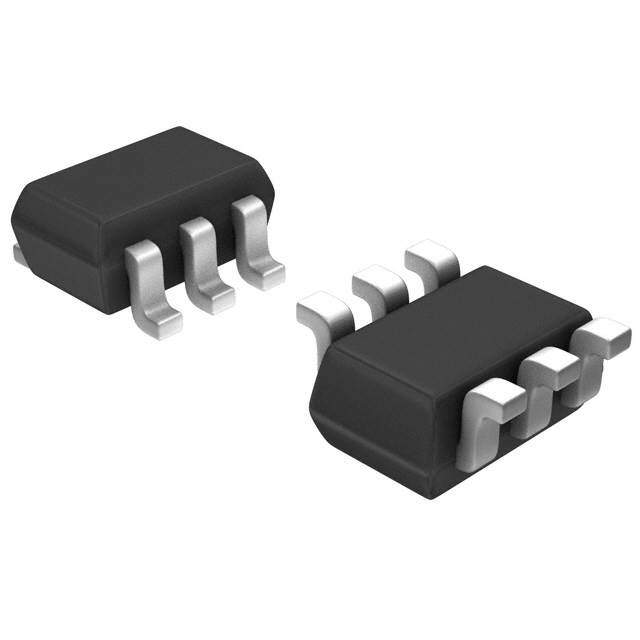
| 描述 | IC MMIC AMP HBT 6GHZ SC-70-6 |
| 产品分类 | RF 放大器 |
| 品牌 | Hittite Microwave Corporation |
| 数据手册 | 点击此处下载产品Datasheet |
| 产品图片 |  |
| P1dB | 12dBm |
| 产品型号 | HMC476SC70E |
| RF类型 | WiMAX / WiBro |
| rohs | 无铅 / 符合限制有害物质指令(RoHS)规范要求 |
| 产品系列 | - |
| 供应商器件封装 | SC-70 |
| 其它名称 | 1127-1413-2 HMC476SC70ETR |
| 包装 | 带卷 (TR) |
| 噪声系数 | 3dB |
| 增益 | 19dB |
| 封装/外壳 | 6-TSSOP,SC-88,SOT-363 |
| 标准包装 | 500 |
| 测试频率 | - |
| 电压-电源 | 5 V ~ 12 V |
| 电流-电源 | 35mA |
| 频率 | 0Hz ~ 6GHz |
Datasheet
PDF Datasheet 数据手册内容提取
HMC476SC70 / 476SC70E v04.0814 SiGe HBT GAiN BLOCK MMiC AMPLiFieR, DC - 6 GHz Typical Applications Features The HMC476SC70(E) is ideal for: P1dB Output Power: +12 dBm T • Cellular / PCS / 3G Gain: 20 dB M • WiBro / WiMAX / 4G Output IP3: +24 dBm S • Fixed Wireless & WLAN Cascadable 50 Ohm I/Os - • CATV, Cable Modem & DBS Single Supply: +5V to +12V K C • Microwave Radio & Test Equipment Industry Standard SC70 Package O L B Functional Diagram General Description N The HMC476SC70(E) is a SiGe Heterojunction Bipolar I A Transistor (HBT) Gain Block MMIC SMT amplifiers G covering DC to 6 GHz. This industry standard SC70 packaged amplifier can be used as a cascadable & 50 Ohm RF/IF gain stage as well as a LO or PA driver R with up to +12 dBm output power. The HMC476SC70(E) E offers 20 dB of gain with a +24 dBm output IP3 at V 850 MHz while requiring only 35 mA from a single I R positive supply. The Darlington topology results in D reduced sensitivity to normal process variations and - excellent gain stability over temperature while requiring S a minimal number of external bias components. R E I F I L P M electrical Specifications, Vs= 5V, Rbias= 56 Ohm, T = +25° C A A Parameter Min. Typ. Max. Units DC - 2.0 GHz 16 19 dB Gain 2.0 - 4.0 GHz 13 16 dB 4.0 - 6.0 GHz 9 12 dB Gain Variation Over Temperature DC - 6 GHz 0.008 0.012 dB/ °C DC - 4 GHz 20 dB Input Return Loss 4.0 - 6.0 GHz 15 dB DC - 4 GHz 20 dB Output Return Loss 4.0 - 6.0 GHz 13 dB Reverse Isolation DC - 6 GHz 18 dB 0.5 - 4.0 GHz 9.0 12.0 dBm Output Power for 1 dB Compression (P1dB) 4.0 - 6.0 GHz 8.0 11.0 dBm Output Third Order Intercept (IP3) 0.5 - 4.0 GHz 24 dBm (Pout= 0 dBm per tone, 1 MHz spacing) 4.0 - 6.0 GHz 22 dBm 0.5 - 4.0 GHz 2.5 dB Noise Figure 4.0 - 6.0 GHz 3.0 dB Supply Current (Icq) 35 42 mA InformationF ofurrn ipshreidc eby, Adnealloigv eDervyic easn isd b teolie vpelda tco eb eo arcdcuerartse :a Andn raelliaobgle. DHoewveivcere, sno, InFco.r, p2r iEceli,z daebliveetrhy , Darnidv eto, Cplhaceel morsdfeorrsd: ,A MnaAlog 0 D18ev2ic4es, Inc., responsibility is assumed by Analog Devices for its use, nor for any infringements of patents or other One Technology Way, P.O. Box 9106, Norwood, MA 02062-9106 1 rliicgehntss eo fi sth girrda nptaerdti ebsy t himatp mlicaaytP iorenhs uoolrt nofrtoehme:r wi9tsis 7ues8 eu-.n 2dSep5re 0cainf-iyc3 apt3iaot4nesn3 ts ou•rb jpeFacttae tnoxt c:r hig9ahn7tgs 8eo wf- 2Aithn5oau0lot g-n 3oDti3ecve7i.c 3eNso .• OPhrdoneer: O78n1--3li2n9e-4 a7t0 0w (cid:127)w Owrd.ehri totnitlien.ec aot mwww.analog.com Trademarks and registered trademarks areA thpe pprolipceartyt oiof tnhe iSr reusppepctoiver to:w nPehrs.one: 978-250-3A3p4pl3ic aotrio an pSpupsp@ohrt:i tPtihteon.ce:o 1m-800-ANALOG-D
HMC476SC70 / 476SC70E v04.0814 SiGe HBT GAiN BLOCK MMiC AMPLiFieR, DC - 6 GHz Broadband Gain & Return Loss Gain vs. Temperature 25 24 20 T 15 20 M 10 RESPONSE (dB)-1-0505 SSS212112 GAIN (dB) 11826 ++2855CC CK - S -15 -40C O -20 4 -25 L -30 0 B 0 1 2 3 4 5 6 7 8 0 1 2 3 4 5 6 N FREQUENCY (GHz) FREQUENCY (GHz) I A G input Return Loss vs. Temperature Output Return Loss vs. Temperature & 0 0 R E -5 -5 V SS (dB)-10 ++-428055CCC SS (dB)-10 ++-428055CCC RI O O D N L-15 N L-15 R R U U - RET-20 RET-20 S R -25 -25 E -30 -30 I F 0 1 2 3 4 5 6 0 1 2 3 4 5 6 I FREQUENCY (GHz) FREQUENCY (GHz) L P M A Reverse isolation vs. Temperature Noise Figure vs. Temperature 0 8 ATION (dB)-1-05 ++-428055CCC RE (dB) 6 ++-428055 CCC L U O-15 G 4 E IS E FI S S VER-20 NOI 2 E R-25 -30 0 0 1 2 3 4 5 6 0 1 2 3 4 5 6 FREQUENCY (GHz) FREQUENCY (GHz) InformationF ofurrn ipshreidc eby, Adnealloigv eDervyic easn isd b teolie vpelda tco eb eo arcdcuerartse :a Andn raelliaobgle. DHoewveivcere, sno, InFco.r, p2r iEceli,z daebliveetrhy , Darnidv eto, Cplhaceel morsdfeorrsd: ,A MnaAlog 0 D18ev2ic4es, Inc., responsibility is assumed by Analog Devices for its use, nor for any infringements of patents or other One Technology Way, P.O. Box 9106, Norwood, MA 02062-9106 rights of third parties that mayP rehsuolt nfroem: i9ts 7us8e-. 2Sp5e0cif-ic3at3io4ns3 s u•b jeFcta tox c: h9an7g8e w-2ith5ou0t -n3oti3ce7. 3No • OPhrdoneer: O78n1--3li2n9e-4 a7t0 0w (cid:127)w Owrd.ehri totnitlien.ec aot mwww.analog.com 2 license is granted by implication or otherwise under any patent or patent rights of Analog Devices. Trademarks and registered trademarks areA thpe pprolipceartyt oiof tnhe iSr reusppepctoiver to:w nPehrs.one: 978-250-3A3p4pl3ic aotrio an pSpupsp@ohrt:i tPtihteon.ce:o 1m-800-ANALOG-D
HMC476SC70 / 476SC70E v04.0814 SiGe HBT GAiN BLOCK MMiC AMPLiFieR, DC - 6 GHz P1dB vs. Temperature Psat vs. Temperature 18 18 T 15 15 M S m) 12 m) 12 K - P1dB (dB 9 +25 C Psat (dB 9 +25C C 6 +85 C 6 +85C -40 C -40C O 3 3 L B 0 0 0 1 2 3 4 5 6 0 1 2 3 4 5 6 N FREQUENCY (GHz) FREQUENCY (GHz) I A G Gain, Power & OiP3 vs. Supply Voltage & Output iP3 vs. Temperature for Constant icc = 35 mA @ 850 MHz R 30 m) 28 B E 3 (d 24 - DRIV IP3 (dBm) 122826 ++2855CC Bm), Psat (dBm), IP 112260 -40C d S dB ( 8 Gain ER 14 B), P1 4 PPIP1s3adtB d I 10 N ( 0 F 0 1 2 3 4 5 6 GAI 5 6 7 8 9 10 LI FREQUENCY (GHz) Vs (Vdc) P M icc vs. Vcc Over Temperature for A Fixed Vs = 5V, Rbias = 56 Ohms 42 +85 C 40 38 +25 C A) m c ( 36 c I 34 -40 C 32 30 2.7 2.8 2.9 3 3.1 3.2 Vcc (V) InformationF ofurrn ipshreidc eby, Adnealloigv eDervyic easn isd b teolie vpelda tco eb eo arcdcuerartse :a Andn raelliaobgle. DHoewveivcere, sno, InFco.r, p2r iEceli,z daebliveetrhy , Darnidv eto, Cplhaceel morsdfeorrsd: ,A MnaAlog 0 D18ev2ic4es, Inc., responsibility is assumed by Analog Devices for its use, nor for any infringements of patents or other One Technology Way, P.O. Box 9106, Norwood, MA 02062-9106 3 rliicgehntss eo fi sth girrda nptaerdti ebsy t himatp mlicaaytP iorenhs uoolrt nofrtoehme:r wi9tsis 7ues8 eu-.n 2dSep5re 0cainf-iyc3 apt3iaot4nesn3 ts ou•rb jpeFacttae tnoxt c:r hig9ahn7tgs 8eo wf- 2Aithn5oau0lot g-n 3oDti3ecve7i.c 3eNso .• OPhrdoneer: O78n1--3li2n9e-4 a7t0 0w (cid:127)w Owrd.ehri totnitlien.ec aot mwww.analog.com Trademarks and registered trademarks areA thpe pprolipceartyt oiof tnhe iSr reusppepctoiver to:w nPehrs.one: 978-250-3A3p4pl3ic aotrio an pSpupsp@ohrt:i tPtihteon.ce:o 1m-800-ANALOG-D
HMC476SC70 / 476SC70E vv0043..00881144 SiGe HBT GAiN BLOCK MMiC AMPLiFieR, DC - 6 GHz Absolute Maximum Ratings Collector Bias Voltage (Vcc) +6V ELECTROSTATIC SENSITIVE DEVICE Collector Bias Current (Icc) 45 mA T RF Input Power (RFIN)(Vcc = +2.4V) +5 dBm OBSERVE HANDLING PRECAUTIONS M Junction Temperature 150 °C S Continuous Pdiss (T = 85 °C) 0.504 W - (derate 7.75 mW/°C above 85 °C) K Thermal Resistance 129 °C/W C (junction to lead) O Storage Temperature -65 to +150 °C L Operating Temperature -40 to +85 °C B ESD Sensitivity (HBM) Class 1A N I A G Outline Drawing & R E V I R D - S R E I F I L P NOTES: M 1. PACKAGE BODY MATERIAL: LOW STRESS INJECTION MOLDED PLASTIC SILICA AND SILICON IMPREGNATED. A 2. LEAD MATERIAL: COPPER ALLOY 3. LEAD PLATING: Sn/Pb 4. DIMENSIONS ARE IN INCHES [MILLIMETERS]. 5. DIMENSION DOES NOT INCLUDE MOLDFLASH OF 0.15mm PER SIDE. 6. DIMENSION DOES NOT INCLUDE MOLDFLASH OF 0.25mm PER SIDE. 7. ALL GROUND LEADS MUST BE SOLDERED TO PCB RF GROUND. Package information Part Number Package Body Material Lead Finish MSL Rating Package Marking HMC476SC70 Low Stress Injection Molded Plastic Sn/Pb MSL1 [1] 476E HMC476SC70E RoHS-compliant Low Stress Injection Molded Plastic 100% matte Sn MSL1 [2] 476E [1] Max peak reflow temperature of 235 °C [2] Max peak reflow temperature of 260 °C InformationF ofurrn ipshreidc eby, Adnealloigv eDervyic easn isd b teolie vpelda tco eb eo arcdcuerartse :a Andn raelliaobgle. DHoewveivcere, sno, InFco.r, p2r iEceli,z daebliveetrhy , Darnidv eto, Cplhaceel morsdfeorrsd: ,A MnaAlog 0 D18ev2ic4es, Inc., responsibility is assumed by Analog Devices for its use, nor for any infringements of patents or other One Technology Way, P.O. Box 9106, Norwood, MA 02062-9106 rights of third parties that mayP rehsuolt nfroem: i9ts 7us8e-. 2Sp5e0cif-ic3at3io4ns3 s u•b jeFcta tox c: h9an7g8e w-2ith5ou0t -n3oti3ce7. 3No • OPhrdoneer: O78n1--3li2n9e-4 a7t0 0w (cid:127)w Owrd.ehri totnitlien.ec aot mwww.analog.com 4 license is granted by implication or otherwise under any patent or patent rights of Analog Devices. Trademarks and registered trademarks areA thpe pprolipceartyt oiof tnhe iSr reusppepctoiver to:w nPehrs.one: 978-250-3A3p4pl3ic aotrio an pSpupsp@ohrt:i tPtihteon.ce:o 1m-800-ANALOG-D
HMC476SC70 / 476SC70E v04.0814 SiGe HBT GAiN BLOCK MMiC AMPLiFieR, DC - 6 GHz Pin Descriptions Pin Number Function Description Interface Schematic T M 1, 2, 4, 5 GND These pins must be connected to RF/DC ground. S - This pin is DC coupled. K 3 RFIN An off chip DC blocking capacitor is required. C O L 6 RFOUT RF output and DC Bias (Vcc) for the output stage. B N I A G Application Circuit & R E V I R D - S R E I F I L P M A Recommended Bias Resistor Values for icc= 35 mA, Rbias= (Vs - Vcc) / icc Supply Voltage (Vs) 5V 8V 10V 12V Note: 1. External blocking capacitors are required on Rbias Value 56 Ω 130 Ω 180 Ω 240 Ω RFIN and RFOUT. Rbias Power rating 1/8 W 1/4 W 1/4 W 1/2 W 2. Rbias provides DC bias stability over temperature. Recommended Component Values for Key Application Frequencies Frequency (MHz) Component 50 900 1900 2200 2400 3500 5200 5800 L1 270 nH 56 nH 18 nH 18 nH 15 nH 8.2 nH 6.8 nH 3.3 nH C1, C2 0.01 µF 100 pF 100 pF 100 pF 100 pF 100 pF 100 pF 100 pF InformationF ofurrn ipshreidc eby, Adnealloigv eDervyic easn isd b teolie vpelda tco eb eo arcdcuerartse :a Andn raelliaobgle. DHoewveivcere, sno, InFco.r, p2r iEceli,z daebliveetrhy , Darnidv eto, Cplhaceel morsdfeorrsd: ,A MnaAlog 0 D18ev2ic4es, Inc., responsibility is assumed by Analog Devices for its use, nor for any infringements of patents or other One Technology Way, P.O. Box 9106, Norwood, MA 02062-9106 5 rliicgehntss eo fi sth girrda nptaerdti ebsy t himatp mlicaaytP iorenhs uoolrt nofrtoehme:r wi9tsis 7ues8 eu-.n 2dSep5re 0cainf-iyc3 apt3iaot4nesn3 ts ou•rb jpeFacttae tnoxt c:r hig9ahn7tgs 8eo wf- 2Aithn5oau0lot g-n 3oDti3ecve7i.c 3eNso .• OPhrdoneer: O78n1--3li2n9e-4 a7t0 0w (cid:127)w Owrd.ehri totnitlien.ec aot mwww.analog.com Trademarks and registered trademarks areA thpe pprolipceartyt oiof tnhe iSr reusppepctoiver to:w nPehrs.one: 978-250-3A3p4pl3ic aotrio an pSpupsp@ohrt:i tPtihteon.ce:o 1m-800-ANALOG-D
HMC476SC70 / 476SC70E v04.0814 SiGe HBT GAiN BLOCK MMiC AMPLiFieR, DC - 6 GHz evaluation PCB T M S - K C O L B N I A G & R E V I R D - S R E I F I L P M List of Materials for evaluation PCB 118038 [1] A The circuit board used in the application should use Item Description RF circuit design techniques. Signal lines should J1 - J2 PCB Mount SMA Connector have 50 Ohm impedance while the package ground J3 - J4 DC Pin leads should be connected directly to the ground C1 - C3 100 pF Capacitor, 0402 Pkg. plane similar to that shown. A sufficient number C4 1000 pF Capacitor, 0603 Pkg. of via holes should be used to connect the top C5 2.2 µF Capacitor, Tantalum and bottom ground planes. The evaluation board R1 50 Ohm Resistor, 1210 Pkg. should be mounted to an appropriate heat sink. The L1 18 nH Inductor, 0603 Pkg. evaluation circuit board shown is available from U1 HMC476SC70(E) Hittite upon request. PCB [2] 117360 Evaluation PCB [1] Reference this number when ordering complete evaluation PCB [2] Circuit Board Material: Rogers 4350 InformationF ofurrn ipshreidc eby, Adnealloigv eDervyic easn isd b teolie vpelda tco eb eo arcdcuerartse :a Andn raelliaobgle. DHoewveivcere, sno, InFco.r, p2r iEceli,z daebliveetrhy , Darnidv eto, Cplhaceel morsdfeorrsd: ,A MnaAlog 0 D18ev2ic4es, Inc., responsibility is assumed by Analog Devices for its use, nor for any infringements of patents or other One Technology Way, P.O. Box 9106, Norwood, MA 02062-9106 rights of third parties that mayP rehsuolt nfroem: i9ts 7us8e-. 2Sp5e0cif-ic3at3io4ns3 s u•b jeFcta tox c: h9an7g8e w-2ith5ou0t -n3oti3ce7. 3No • OPhrdoneer: O78n1--3li2n9e-4 a7t0 0w (cid:127)w Owrd.ehri totnitlien.ec aot mwww.analog.com 6 license is granted by implication or otherwise under any patent or patent rights of Analog Devices. Trademarks and registered trademarks areA thpe pprolipceartyt oiof tnhe iSr reusppepctoiver to:w nPehrs.one: 978-250-3A3p4pl3ic aotrio an pSpupsp@ohrt:i tPtihteon.ce:o 1m-800-ANALOG-D