首页 > HMC463LP5E > 详情
 Datasheet下载
- 型号: HMC463LP5E
- 制造商: Hittite
- 库位|库存: xxxx|xxxx
- 要求:
| 数量阶梯 | 香港交货 | 国内含税 |
| +xxxx | $xxxx | ¥xxxx |
查看当月历史价格
查看今年历史价格
产品参数
| 参数 | 数值 |
| 产品目录 | 射频/IF 和 RFID |
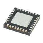
| 描述 | IC MMIC AMP AGC LNA 32-QFN |
| 产品分类 | RF 放大器 |
| 品牌 | Hittite Microwave Corporation |
| 数据手册 | 点击此处下载产品Datasheet |
| 产品图片 |  |
| P1dB | 16dBm |
| 产品型号 | HMC463LP5E |
| RF类型 | 通用 |
| rohs | 无铅 / 符合限制有害物质指令(RoHS)规范要求 |
| 产品系列 | - |
| 供应商器件封装 | 32-QFN(5x5) |
| 其它名称 | 1127-1402-6 |
| 包装 | Digi-Reel® |
| 噪声系数 | 3dB |
| 增益 | 12dB |
| 封装/外壳 | 32-VFQFN 裸露焊盘 |
| 标准包装 | 1 |
| 测试频率 | 6GHz ~ 18GHz |
| 特色产品 | http://www.digikey.cn/product-highlights/zh/wideband-distributed-amplifiers/52879 |
| 电压-电源 | 5V |
| 电流-电源 | 60mA |
| 频率 | 2GHz ~ 20GHz |
Datasheet
PDF Datasheet 数据手册内容提取
HMC463LP5 463LP5E / v09.0717 GaAs pHEMT MMIC LOW NOISE AGC AMPLIFIER, 2 - 20 GHz 7 Typical Applications Features The HMC463LP5(E) is ideal for: Gain: 13 dB T M • Telecom Infrastructure Noise Figure: 2.8 dB @ 10 GHz S • Microwave Radio & VSAT P1dB Output Power: +18 dBm @ 10 GHz - • Military EW, ECM & C3I Supply Voltage: +5V @ 60mA E • Test Instrumentation 50 Ohm Matched Input/Output S I • Fiber Optics 32 Lead 5x5mm SMT Package: 25mm² O N W Functional Diagram General Description O The HMC463LP5(E) is a GaAs MMIC pHEMT Low L Noise AGC Distributed Amplifier packaged in a lead- - less 5x5 mm surface mount package which oper- S ates between 2 and 20 GHz. The amplifier provides R 13 dB of gain, 2.8 dB noise figure and 18 dBm of out- E put power at 1 dB gain compression while requiring I F only 60mA from a +5V supply. An optional gate bias I L (Vgg2) is provided to allow Adjustable Gain Control P (AGC) of 8 dB typical. Gain flatness is excellent at M ±0.5 dB from 6 - 18 GHz making the HMC463LP5(E) A ideal for EW, ECM RADAR and test equipment appli- cations. The HMC463LP5(E) LNA I/Os are internally matched to 50 Ohms and are internally DC blocked. Electrical Specifications, T = +25 °C, Vdd = 5V, Idd = 60 mA* A Parameter Min. Typ. Max. Min. Typ. Max. Min. Typ. Max. Units Frequency Range 2 - 6 6 - 18 18 - 20 GHz Gain 10 13 9 12 8 11 dB Gain Flatness ±0.5 ±0.5 ±0.5 dB Gain Variation Over Temperature 0.010 0.015 0.010 0.015 0.010 0.015 dB/ °C Noise Figure 3 4 3 5 5.5 6.5 dB Input Return Loss 15 13 12 dB Output Return Loss 13 10 10 dB Output Power for 1 dB Compression 16 19 11 16 10 12 dBm (P1dB) Saturated Output Power (Psat) 21 19 19 dBm Output Third Order Intercept (IP3) 30 24 22 dBm Supply Current 60 80 60 80 60 80 mA (Idd) (Vdd = 5V, Vgg1 = -0.9V Typ.) * Adjust Vgg1 between -2 to -0V to achieve Idd = 60 mA typical. InFforomra ptiorni cfuer,n idsheeldi vbey rAy,n aalongd D teovi cpelsa ics eb eolierdveed rtso: bAen aaclcourga teD aenvdi creelisab, leIn. cHo.,w Oevenre, nTo echFnoro lporgicye ,W daeyli,v ePr.yO, .a Bndo xto 9 1p0la6c,e Noordrweros:o dAn, aMloAg 0D2e0v6ic2e-s9, 1I0nc6., responsibility is assumed by Analog Devices for its uPseh, ononre fo:r 7an8y1 in-f3ri2ng9e-m4e7nt0s 0of •pa Otenrtds eorr o othnerl ineO ante wTewcwhn.aolnoaglyo Wg.acyo, mP.O. Box 9106, Norwood, MA 02062-9106 7 - 1 rliicgehntss eo fi sth girrda nptaerdti ebsy t himatp mlicaayt iroens uolrt fortohme riwtsi sues eu.n Sdpeer caifinyc aptiaAotnepsn pts oulirbc jpeaacttte itonot n crhi gSahntugs peo wfp Aiotnhraotluo:t g Pn oDhteicoveinc. eNeso:. 1-P8h0o0n-eA: N78A1L-O32G9--4D700 • Order online at www.analog.com Trademarks and registered trademarks are the property of their respective owners. Application Support: Phone: 1-800-ANALOG-D
HMC463LP5 / 463LP5E v09.0717 GaAs pHEMT MMIC LOW NOISE AGC AMPLIFIER, 2 - 20 GHz 7 Gain & Return Loss Gain vs. Temperature 20 20 T 15 M 10 16 B) 5 S21 S d S11 ESPONSE ( -1-005 S22 GAIN (dB) 128 SE - R -15 I +25C O -20 4 +85C -40C N -25 -30 0 W 0 2 4 6 8 10 12 14 16 18 20 22 0 2 4 6 8 10 12 14 16 18 20 22 FREQUENCY (GHz) FREQUENCY (GHz) O L - S Input Return Loss vs. Temperature Output Return Loss vs. Temperature R 0 0 E S (dB)-1-05 ++-428055CCC S (dB) -5 ++-428055CCC PLIFI S S O O N L-15 N L -10 M R R U U A ET-20 ET R R -15 -25 -30 -20 0 2 4 6 8 10 12 14 16 18 20 22 0 2 4 6 8 10 12 14 16 18 20 22 FREQUENCY (GHz) FREQUENCY (GHz) Reverse Isolation vs. Temperature Noise Figure vs. Temperature 0 10 +25C -10 +-4805CC 8 ++2855CC B) -40C OLATION (dB) --3200 SE FIGURE (d 46 IS -40 NOI 2 -50 -60 0 0 2 4 6 8 10 12 14 16 18 20 22 0 2 4 6 8 10 12 14 16 18 20 22 FREQUENCY (GHz) FREQUENCY (GHz) For price, delivery, and to place orders: Analog Devices, Inc., One Technology Way, P.O. Box 9106, Norwood, MA 02062-9106 Phone: 781-329-4700 • Order online at www.analog.com 7 - 2 Application Support: Phone: 1-800-ANALOG-D
HMC463LP5 / 463LP5E v09.0717 GaAs pHEMT MMIC LOW NOISE AGC AMPLIFIER, 2 - 20 GHz 7 P1dB vs. Temperature Psat vs. Temperature 26 26 T M 22 22 S SE - P1dB (dBm) 1148 Psat (dBm) 1148 ++-428055CCC I O +25C 10 +85C 10 N -40C 6 6 W 0 2 4 6 8 10 12 14 16 18 20 22 0 2 4 6 8 10 12 14 16 18 20 22 O FREQUENCY (GHz) FREQUENCY (GHz) L - Gain, Power & Noise Figure S Output IP3 vs. Temperature vs. Supply Voltage @ 10 GHz, Fixed Vgg1 R 32 24 4.5 E I m) 22 4 F 29 dB I at ( 20 3.5 L s N AMP IP3 (dBm) 2236 1dB (dBm), P 111468 223.5 OISE FIGUR 1270 ++-428055CCC GAIN (dB), P 11028 NOISE FIGURE PGP1sadainBt 011..55 E (dB) 14 6 0 0 2 4 6 8 10 12 14 16 18 20 22 4.5 5 5.5 FREQUENCY (GHz) Vdd (V) Gain, P1dB & Output IP3 Noise Figure & Supply Current vs. Control Voltage @ 10 GHz vs. Control Voltage @ 10 GHz 32 75 5.5 m) 28 70 5 B d 65 4.5 P3 ( 24 60 4 AIN (dB), P1dB (dBm), I 11226048 GP1adinB Idd (mA) 334455050505 112233...555 NOISE FIGURE (dB) G 0 IP3 25 Idd NOISE FIGURE 0.5 -4 20 0 -1.4 -1.2 -1 -0.8 -0.6 -0.4 -0.2 0 0.2 0.4 0.6 0.8 1 -1.4 -1.2 -1 -0.8 -0.6 -0.4 -0.2 0 0.2 0.4 0.6 0.8 1 Vgg2 (V) Vgg2 (V) For price, delivery, and to place orders: Analog Devices, Inc., One Technology Way, P.O. Box 9106, Norwood, MA 02062-9106 Phone: 781-329-4700 • Order online at www.analog.com 7 - 3 Application Support: Phone: 1-800-ANALOG-D
HMC463LP5 / 463LP5E v09.0717 GaAs pHEMT MMIC LOW NOISE AGC AMPLIFIER, 2 - 20 GHz 7 Gain @ Several Control Voltages (Vgg2) Absolute Maximum Ratings 18 Drain Bias Voltage (Vdd) +9V T 13 Gate Bias Voltage (Vgg1) -2 to 0V M Gate Bias Current (Igg1) 2.5 mA S 8 Gate Bias Voltage (Vgg2)(AGC) (Vdd -9) Vdc to +2V dB) - GAIN ( 3 RCFha Innnpeult TPeomwpeer r(aRtuFrIeN)(Vdd = +5V) +15108 °dCBm E S -2 Vgg2 = -1.3V Vgg2 = -0.8V Continuous Pdiss (T= 85 °C) Vgg2 = -1.2V Vgg2 = -0.6V 1.24 W I Vgg2 = -1.1V Vgg2 = -0.4V (derate 19.1 mW/°C above 85 °C) O -7 VVgggg22 == --10..09VV VVgggg22 == -00V.2V Thermal Resistance N 52.3 °C/W (channel to ground paddle) -12 W 0 2 4 6 8 10 12 14 16 18 20 22 Storage Temperature -65 to +150 °C FREQUENCY (GHz) Operating Temperature -40 to +85 °C O Class 0B - Passed L ESD Sensitivity (HBM) 150V - ELECTROSTATIC SENSITIVE DEVICE S OBSERVE HANDLING PRECAUTIONS R Typical Supply Current vs. Vdd E I Vdd (V) Idd (mA) F +4.5 58 I L +5.0 60 P +5.5 62 M A For price, delivery, and to place orders: Analog Devices, Inc., One Technology Way, P.O. Box 9106, Norwood, MA 02062-9106 Phone: 781-329-4700 • Order online at www.analog.com 7 - 4 Application Support: Phone: 1-800-ANALOG-D
HMC463LP5 / 463LP5E v09.0717 GaAs pHEMT MMIC LOW NOISE AGC AMPLIFIER, 2 - 20 GHz 7 32-Lead Lead Frame Chip Scale Package [LFCSP] Outline Drawing 5 x 5 mm Body and 0.90 mm Package Height (HCP-32-1) Dimensions shown in millimeters T DETAIL A M (JEDEC 95) 5.10 0.30 S 5.00 SQ 0.25 PIN 1 4.90 0.18 PIN 1 - INDICATOR 25 32 I(NSEDEIC DAETTAOIRL AA)R EA OPTIONS E 24 1 0.50 S BSC EXPOSED 3.80 I PAD 3.70 SQ O 3.60 N 17 8 W TOP VIEW 00..4450 16 BOTTOM VIEW 9 0.20 MIN 0.35 3.50 REF O 0.90 L 0.85 0.05 MAX FTOHER EPXRPOOPSEERD C POANDN, ERCETFIEORN TOOF 0.80 0.02 NOM TFHUEN CPTINIO CNO DNEFSIGCURRIPATTIOIONNS A ND - COPLANARITY SECTION OF THIS DATA SHEET. 0.08 S SEATING 0.20 REF PLANE IER PKG-004898 COMPLIANT TO JEDEC STANDARDS MO-220-VHHD-4. 03-09-2017-B F I 32-Lead Lead Frame Chip Scale Package [LFCSP] L 5 mm × 5 mm Body and 0.90 mm Package Height P (HCP-32-1) M Dimensions shown in millimeters A Package Information Part Number Package Body Material Lead Finish MSL Rating Package Marking [3] HMC463LP5 Low Stress Injection Molded Plastic Sn/Pb Solder MSL1 [1] H463 XXXX HMC463LP5E RoHS-compliant Low Stress Injection Molded Plastic 100% matte Sn MSL1 [2] H463 XXXX [1] Max peak reflow temperature of 235 °C [2] Max peak reflow temperature of 260 °C [3] 4-Digit lot number XXXX For price, delivery, and to place orders: Analog Devices, Inc., One Technology Way, P.O. Box 9106, Norwood, MA 02062-9106 Phone: 781-329-4700 • Order online at www.analog.com 7 - 5 Application Support: Phone: 1-800-ANALOG-D
HMC463LP5 / 463LP5E v09.0717 GaAs pHEMT MMIC LOW NOISE AGC AMPLIFIER, 2 - 20 GHz 7 Pin Descriptions Pin Number Function Description Interface Schematic T 1, 3, 4, 6-14, The pins are not connected internally; however, all data M 16-20, 22-29, N/C shown herein was measured with these pins connected to S 31, 32 RF/DC ground externally. - E S Optional gate control if AGC is required. I 2 Vgg2 Leave Vgg2 open circuited if AGC is not required. O Typical Vgg2 = -1.5V to 0V N W O 5 RFIN This pad is AC coupled and matched to 50 Ohms L - S 15 Vgg1 Gate control for amplifier. Adjust to achieve Idd = 60mA. R E I F I 21 RFOUT This pad is AC coupled and matched to 50 Ohms L P M Power supply voltage for the amplifier. A 30 Vdd External bypass capacitors are required Ground GND Ground paddle must be connected to RF/DC ground. Paddle For price, delivery, and to place orders: Analog Devices, Inc., One Technology Way, P.O. Box 9106, Norwood, MA 02062-9106 Phone: 781-329-4700 • Order online at www.analog.com 7 - 6 Application Support: Phone: 1-800-ANALOG-D
HMC463LP5 / 463LP5E v09.0717 GaAs pHEMT MMIC LOW NOISE AGC AMPLIFIER, 2 - 20 GHz 7 Application Circuit T M S - E S I O N W O L - S R E I F I L P M A For price, delivery, and to place orders: Analog Devices, Inc., One Technology Way, P.O. Box 9106, Norwood, MA 02062-9106 Phone: 781-329-4700 • Order online at www.analog.com 7 - 7 Application Support: Phone: 1-800-ANALOG-D
HMC463LP5 / 463LP5E v09.0717 GaAs pHEMT MMIC LOW NOISE AGC AMPLIFIER, 2 - 20 GHz 7 Evaluation PCB T M S - E S I O N W O L - S R E I F I L P M A List of Materials for Evaluation PCB 108341 [1] The circuit board used in the application should Item Description use RF circuit design techniques. Signal lines J1 - J2 SRI K Connector should have 50 Ohm impedance while the package J3 - J4 2 mm Molex Header ground leads and package bottom should be C1 - C3 100 pF Capacitor, 0402 Pkg. connected directly to the ground plane similar to C4 - C6 1000 pF Capacitor, 0603 Pkg. that shown. A sufficient number of via holes should C7 - C8 4.7 µF Capacitor, Tantalum be used to connect the top and bottom ground U1 HMC463LP5(E) Amplifier planes. The evaluation board should be mounted PCB [2] 109949 Evaluation PCB to an appropriate heat sink. The evaluation circuit [1] Reference this number when ordering complete evaluation PCB board shown is available from Analog Devices [2] Circuit Board Material: Rogers 4350 or Arlon 25FR upon request. For price, delivery, and to place orders: Analog Devices, Inc., One Technology Way, P.O. Box 9106, Norwood, MA 02062-9106 Phone: 781-329-4700 • Order online at www.analog.com 7 - 8 Application Support: Phone: 1-800-ANALOG-D
Mouser Electronics Authorized Distributor Click to View Pricing, Inventory, Delivery & Lifecycle Information: A nalog Devices Inc.: HMC463LP5E HMC463LP5ETR HMC463LP5