首页 > HMC453ST89E > 详情
 Datasheet下载
- 型号: HMC453ST89E
- 制造商: Hittite
- 库位|库存: xxxx|xxxx
- 要求:
| 数量阶梯 | 香港交货 | 国内含税 |
| +xxxx | $xxxx | ¥xxxx |
查看当月历史价格
查看今年历史价格
产品参数
| 参数 | 数值 |
| 产品目录 | 射频/IF 和 RFID |
| 描述 | IC MMIC AMP HBT 1.6W SOT-89 |
| 产品分类 | RF 放大器 |
| 品牌 | Hittite Microwave Corporation |
| 数据手册 | 点击此处下载产品Datasheet |
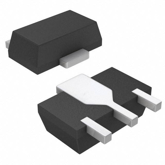
| 产品图片 |  |
| P1dB | 32.5dBm |
| 产品型号 | HMC453ST89E |
| RF类型 | 通用 |
| rohs | 无铅 / 符合限制有害物质指令(RoHS)规范要求 |
| 产品系列 | - |
| 供应商器件封装 | SOT-89 |
| 其它名称 | 1127-1396-6 |
| 包装 | Digi-Reel® |
| 噪声系数 | 6.5dB |
| 增益 | 7.5dB |
| 封装/外壳 | TO-243AA |
| 标准包装 | 1 |
| 测试频率 | 2.11GHz |
| 电压-电源 | 5V |
| 电流-电源 | 725mA |
| 频率 | 400MHz ~ 2.2GHz |
Datasheet
PDF Datasheet 数据手册内容提取
HMC453ST89 453ST89E / v02.0710 InGaP HBT 1.6 WATT POWER AMPLIFIER, 0.4 - 2.2 GHz Typical Applications Features The HMC453ST89 / HMC453ST89E is ideal for Output IP3: +49 dBm applications requiring a high dynamic range amplifi er: 20.5 dB Gain @ 400 MHz • GSM, GPRS & EDGE 7.5 dB Gain @ 2100 MHz • CDMA & W-CDMA 41% PAE @ +32.5 dBm Pout • CATV/Cable Modem 9 +26 dBm CDMA2000 • Fixed Wireless Channel Power @ -45 dBc ACP Included in the HMC-DK002 Designer’s Kit T M Functional Diagram General Description S - The HMC453ST89 & HMC453ST89E are high R dynamic range GaAs InGaP HBT 1.6 Watt MMIC power E amplifi ers operating from 0.4 to 2.2 GHz and packaged W in industry standard SOT89 packages. Utilizing a O minimum number of external components and a single P +5V supply, the amplifi er output IP3 can be optimized to +47 dBm at 0.4 GHz or +49 dBm at 2.1 GHz. The & high output IP3 and PAE make the HMC453ST89 & R HMC453ST89E ideal power amplifi ers for Cellular/ A PCS/3G and Fixed Wireless applications. E N I L - S Electrical Specifi cations, T = +25°C, Vs= +5V [1] R A E Parameter Min. Typ. Max. Min. Typ. Max Min. Typ. Max. Min. Typ. Max. Min. Typ. Max. Units I F Frequency Range 400 - 410 450 - 496 810 - 960 1710 - 1990 2010 - 2170 MHz I L Gain 18 20.5 16.5 19 12 14.5 6 8.5 6 7.5 dB P Gain Variation Over dB / 0.012 0.02 0.012 0.02 0.012 0.02 0.012 0.02 0.012 0.02 M Temperature °C A Input Return Loss 20 14 20 15 13 dB Output Return Loss 12 12 13 15 18 dB Output Power for 1dB 28.5 31.5 29 32 28.5 31.5 29 32 29.5 32.5 dBm Compression (P1dB) Saturated Output 32 32.25 31.75 32.5 32.75 dBm Power (Psat) Output Third Order 44 47 45 48 44 47 46 49 46 49 dBm Intercept (IP3) [2] Noise Figure 9 9 6.5 7 6.5 dB Supply Current (Icq) 725 725 725 725 725 mA [1] Specifi cations and data refl ect HMC453ST89 measured using the respective application circuits for each designated frequency band found herein. Contact the HMC Applications Group for assistance in optimizing performance for your application. [2] Two-tone input power of 0 dBm per tone, 1 MHz spacing. InforFmaotiro np fruircniseh,e dd beyl iAvnealroyg Daenvidce st ois pbelaliecveed otor dbee arcsc:u rHateit taintde reMliaibcler. oHwowaevveer, Cnoo rpFoorr aptriiocen,, d2e0liv Aerlyp, haand R too apdla,c Ce horedlemrss: fAonrdal,o gM DAe v0ic1e8s2, 4Inc., responsibility is assumed by Analog Devices for its use, nor for any infringements of patents or other One Technology Way, P.O. Box 9106, Norwood, MA 02062-9106 9 - 168 rliicgehntss eo fi sth girrda nptaerdti ebsy t himatp mlicaaPyt iorhenso uonlrt ofertoh:m e9r wit7sis 8ues -eu2.n dS5epr0e ca-inf3iyc 3aptia4otne3sn ts ou rb jpeFacttae tnoxt c:r hig9ahn7tgs 8eo wf- 2Aithn5oau0lot g-n 3oDti3ecve7i.c 3eNso . POhrodnee:r 7 O81n-3-2li9n-e4 7a0t0 w(cid:127) Owrwde.hr oitntliitnee. cato wmww.analog.com Trademarks and registered trademarks arAe tphep plriocpearttyi oof nth eSir urespppecotivret :o wPnehrso.ne: 978-250-3A3p4p3li c aotrio na Spuppsp@orht: iPtthitoen.ec: o1-m800-ANALOG-D
HMC453ST89 / 453ST89E v02.0710 InGaP HBT 1.6 WATT POWER AMPLIFIER, 0.4 - 2.2 GHz Broadband Gain & Return Loss @ 400 Gain vs. Temperature @ 400 MHz 25 23 20 22 15 21 20 B) 10 S21 d S11 19 NSE ( 05 S22 N (dB) 18 SPO -5 GAI 17 +25 C 9 E 16 +85 C R -10 15 -40 C -15 14 -20 13 T -25 12 0.1 0.2 0.3 0.4 0.5 0.6 0.7 0.35 0.37 0.39 0.41 0.43 0.45 M FREQUENCY (GHz) FREQUENCY (GHz) S - Input Return Loss Output Return Loss R vs. Temperature @ 400 MHz vs. Temperature @ 400 MHz E W 0 0 O -5 -5 P B) B) SS (d -10 ++2855 CC SS (d -10 & O -40 C O N L N L -15 R UR -15 UR A RET RET -20 E -20 +25 C N -25 +85 C -40 C I L -25 -30 0.35 0.37 0.39 0.41 0.43 0.45 0.35 0.37 0.39 0.41 0.43 0.45 - FREQUENCY (GHz) FREQUENCY (GHz) S R E I P1dB vs. Temperature @ 400 MHz Psat vs. Temperature @ 400 MHz F I 34 34 L P 33 33 M 32 32 31 31 A m) 30 m) 30 P1dB (dB 2289 ++2855 CC Psat (dB 2289 ++2855 CC 27 -40 C 27 -40 C 26 26 25 25 24 24 0.35 0.37 0.39 0.41 0.43 0.45 0.35 0.37 0.39 0.41 0.43 0.45 FREQUENCY (GHz) FREQUENCY (GHz) InforFmaotiro np fruircniseh,e dd beyl iAvnealroyg Daenvidce st ois pbelaliecveed otor dbee arcsc:u rHateit taintde reMliaibcler. oHwowaevveer, Cnoo rpFoorr aptriiocen,, d2e0liv Aerlyp, haand R too apdla,c Ce horedlemrss: fAonrdal,o gM DAe v0ic1e8s2, 4Inc., responsibility is assumed by Analog Devices for its use, nor for any infringements of patents or other One Technology Way, P.O. Box 9106, Norwood, MA 02062-9106 rights of third parties that maPy rhesounlt fero:m 9 it7s 8us-e2. S5p0ec-if3ic3ati4on3s s u b jeFcta tox c: h9an7g8e w-2ith5ou0t -n3oti3ce7. 3No POhrodnee:r 7 O81n-3-2li9n-e4 7a0t0 w(cid:127) Owrwde.hr oitntliitnee. cato wmww.analog.com 9 - 169 license is granted by implication or otherwise under any patent or patent rights of Analog Devices. Trademarks and registered trademarks arAe tphep plriocpearttyi oof nth eSir urespppecotivret :o wPnehrso.ne: 978-250-3A3p4p3li c aotrio na Spuppsp@orht: iPtthitoen.ec: o1-m800-ANALOG-D
HMC453ST89 / 453ST89E v02.0710 InGaP HBT 1.6 WATT POWER AMPLIFIER, 0.4 - 2.2 GHz Noise Figure Output IP3 vs. Temperature @ 400 MHz vs. Temperature @ 400 MHz 52 11 50 10 48 9 46 B) 8 d m) 44 E ( 7 9 OIP3 (dB 344802 ++-428055 CCC SE FIGUR 456 ++-428055 CCC OI 36 N 3 34 2 32 1 T 30 0 M 0.35 0.37 0.39 0.41 0.43 0.45 0.35 0.37 0.39 0.41 0.43 0.45 S FREQUENCY (GHz) FREQUENCY (GHz) - R Reverse Isolation Gain, Power & IP3 E vs. Temperature @ 400 MHz vs. Supply Voltage @ 400 MHz W 0 m) 55 B O 3 (d 50 -5 P P OI 45 AR & OLATION (dB) --1150 ++-428055 CCC m), Psat (dBm), 334050 PGPO1saIdPainBt3 NE IS -20 dB (dB 2205 -25 P1 LI B), 15 d -30 N ( 10 - 0.35 0.37 0.39 0.41 0.43 0.45 AI 4.5 4.75 5 5.25 5.5 G S FREQUENCY (GHz) Vs (Vdc) R E ACPR vs. Supply Voltage @ 400 MHz I F Power Compression @ 400 MHz W-CDMA, 64 DPCH I L 45 -10 P -15 AM B), PAE (%) 334050 GPPoAauiEnt c) ---322050 WFI6n4rt-ee CDqgDuPraeMCtniHAocny: B4W00: 3M.8H4z MHz ain (d 25 R (dB --4305 4.5V G 20 P 5V Bm), 15 AC --5405 5.5V d ut ( 10 -55 o -60 P 5 -65 Source ACPR 0 -70 0 2 4 6 8 10 12 14 16 8 10 12 14 16 18 20 22 24 26 28 INPUT POWER (dBm) Channel Power (dBm) InforFmaotiro np fruircniseh,e dd beyl iAvnealroyg Daenvidce st ois pbelaliecveed otor dbee arcsc:u rHateit taintde reMliaibcler. oHwowaevveer, Cnoo rpFoorr aptriiocen,, d2e0liv Aerlyp, haand R too apdla,c Ce horedlemrss: fAonrdal,o gM DAe v0ic1e8s2, 4Inc., responsibility is assumed by Analog Devices for its use, nor for any infringements of patents or other One Technology Way, P.O. Box 9106, Norwood, MA 02062-9106 9 - 170 rliicgehntss eo fi sth girrda nptaerdti ebsy t himatp mlicaaPyt iorhenso uonlrt ofertoh:m e9r wit7sis 8ues -eu2.n dS5epr0e ca-inf3iyc 3aptia4otne3sn ts ou rb jpeFacttae tnoxt c:r hig9ahn7tgs 8eo wf- 2Aithn5oau0lot g-n 3oDti3ecve7i.c 3eNso . POhrodnee:r 7 O81n-3-2li9n-e4 7a0t0 w(cid:127) Owrwde.hr oitntliitnee. cato wmww.analog.com Trademarks and registered trademarks arAe tphep plriocpearttyi oof nth eSir urespppecotivret :o wPnehrso.ne: 978-250-3A3p4p3li c aotrio na Spuppsp@orht: iPtthitoen.ec: o1-m800-ANALOG-D
HMC453ST89 / 453ST89E v02.0710 InGaP HBT 1.6 WATT POWER AMPLIFIER, 0.4 - 2.2 GHz Broadband Gain & Return Loss @ 470 MHz Gain vs. Temperature @ 470 MHz 25 23 22 20 21 15 20 B) ESPONSE (d 1050 SSS212112 GAIN (dB) 11116789 9 R +25 C -5 15 +85 C -40 C 14 -10 13 T -15 12 0.1 0.2 0.3 0.4 0.5 0.6 0.7 0.43 0.45 0.47 0.49 0.51 0.53 M FREQUENCY (GHz) FREQUENCY (GHz) S - Input Return Loss Output Return Loss R vs. Temperature @ 470 MHz vs. Temperature @ 470 MHz E W 0 0 O dB) -5 ++-428055 CCC dB) -5 ++-428055 CCC P S ( S ( & S S O O N L -10 N L -10 R R R U U A T T RE RE E -15 -15 N I L -20 -20 0.43 0.45 0.47 0.49 0.51 0.53 0.43 0.45 0.47 0.49 0.51 0.53 - FREQUENCY (GHz) FREQUENCY (GHz) S R E I P1dB vs. Temperature @ 470 MHz Psat vs. Temperature @ 470 MHz F I 34 34 L P 33 33 M 32 32 31 31 A m) 30 m) 30 P1dB (dB 2289 ++2855 CC Psat (dB 2289 ++2855 CC 27 -40 C 27 -40 C 26 26 25 25 24 24 0.43 0.45 0.47 0.49 0.51 0.53 0.43 0.45 0.47 0.49 0.51 0.53 FREQUENCY (GHz) FREQUENCY (GHz) InforFmaotiro np fruircniseh,e dd beyl iAvnealroyg Daenvidce st ois pbelaliecveed otor dbee arcsc:u rHateit taintde reMliaibcler. oHwowaevveer, Cnoo rpFoorr aptriiocen,, d2e0liv Aerlyp, haand R too apdla,c Ce horedlemrss: fAonrdal,o gM DAe v0ic1e8s2, 4Inc., responsibility is assumed by Analog Devices for its use, nor for any infringements of patents or other One Technology Way, P.O. Box 9106, Norwood, MA 02062-9106 rights of third parties that maPy rhesounlt fero:m 9 it7s 8us-e2. S5p0ec-if3ic3ati4on3s s u b jeFcta tox c: h9an7g8e w-2ith5ou0t -n3oti3ce7. 3No POhrodnee:r 7 O81n-3-2li9n-e4 7a0t0 w(cid:127) Owrwde.hr oitntliitnee. cato wmww.analog.com 9 - 171 license is granted by implication or otherwise under any patent or patent rights of Analog Devices. Trademarks and registered trademarks arAe tphep plriocpearttyi oof nth eSir urespppecotivret :o wPnehrso.ne: 978-250-3A3p4p3li c aotrio na Spuppsp@orht: iPtthitoen.ec: o1-m800-ANALOG-D
HMC453ST89 / 453ST89E v02.0710 InGaP HBT 1.6 WATT POWER AMPLIFIER, 0.4 - 2.2 GHz Noise Figure Output IP3 vs. Temperature @ 470 MHz vs. Temperature @ 470 MHz 52 11 50 10 48 9 46 B) 8 d m) 44 E ( 7 9 OIP3 (dB 344802 ++-428055 CCC SE FIGUR 456 ++-428055 CCC OI 36 N 3 34 2 32 1 T 30 0 M 0.43 0.45 0.47 0.49 0.51 0.53 0.43 0.45 0.47 0.49 0.51 0.53 S FREQUENCY (GHz) FREQUENCY (GHz) - R Reverse Isolation Gain, Power & IP3 E vs. Temperature @ 470 MHz vs. Supply Voltage @ 470 MHz W 0 m) 50 B O 3 (d 45 R & P TION (dB) --11-505 ++-428055 CCC Psat (dBm), OIP 334050 PGPO1saIdPainBt3 A OLA m), 25 E IS -20 B (dB 20 N -25 P1d LI dB), 15 -30 N ( 10 - 0.43 0.45 0.47 0.49 0.51 0.53 AI 4.5 4.75 5 5.25 5.5 G S FREQUENCY (GHz) Vs (Vdc) R E ACPR vs. Supply Voltage @ 470 MHz I F Power Compression @ 470 MHz W-CDMA, 64 DPCH I L 50 -10 P 45 -15 M %) -20 A dB), PAE ( 334050 GPPoAauiEnt Bc) ---332505 WFI6n4rt-ee CDqgDuPraeMCtniHAocny: B4W70: 3M.8H4z MHz Gain ( 25 PR (d -40 4.5V m), 20 AC -45 5V 5.5V dB 15 -50 ut ( 10 -55 Po -60 5 -65 Source ACPR 0 -70 0 2 4 6 8 10 12 14 16 8 10 12 14 16 18 20 22 24 26 28 INPUT POWER (dBm) Channel Power (dBm) InforFmaotiro np fruircniseh,e dd beyl iAvnealroyg Daenvidce st ois pbelaliecveed otor dbee arcsc:u rHateit taintde reMliaibcler. oHwowaevveer, Cnoo rpFoorr aptriiocen,, d2e0liv Aerlyp, haand R too apdla,c Ce horedlemrss: fAonrdal,o gM DAe v0ic1e8s2, 4Inc., responsibility is assumed by Analog Devices for its use, nor for any infringements of patents or other One Technology Way, P.O. Box 9106, Norwood, MA 02062-9106 9 - 172 rliicgehntss eo fi sth girrda nptaerdti ebsy t himatp mlicaaPyt iorhenso uonlrt ofertoh:m e9r wit7sis 8ues -eu2.n dS5epr0e ca-inf3iyc 3aptia4otne3sn ts ou rb jpeFacttae tnoxt c:r hig9ahn7tgs 8eo wf- 2Aithn5oau0lot g-n 3oDti3ecve7i.c 3eNso . POhrodnee:r 7 O81n-3-2li9n-e4 7a0t0 w(cid:127) Owrwde.hr oitntliitnee. cato wmww.analog.com Trademarks and registered trademarks arAe tphep plriocpearttyi oof nth eSir urespppecotivret :o wPnehrso.ne: 978-250-3A3p4p3li c aotrio na Spuppsp@orht: iPtthitoen.ec: o1-m800-ANALOG-D
HMC453ST89 / 453ST89E v02.0710 InGaP HBT 1.6 WATT POWER AMPLIFIER, 0.4 - 2.2 GHz Broadband Gain & Return Loss @ 900 MHz Gain vs. Temperature @ 900 MHz 20 18 15 17 16 10 B) 15 ESPONSE (d -505 SSS212112 GAIN (dB) 111234 +25C 9 R 11 +85C -10 10 -40C -15 9 T -20 8 0.4 0.5 0.6 0.7 0.8 0.9 1 1.1 1.2 1.3 1.4 0.7 0.75 0.8 0.85 0.9 0.95 1 1.05 1.1 M FREQUENCY (GHz) FREQUENCY (GHz) S - Input Return Loss Output Return Loss R vs. Temperature @ 900 MHz vs. Temperature @ 900 MHz E W 0 0 O -5 +25C +25C P B) +85C B) -5 +85C S (d -10 -40C S (d -40C & S S O O N L -15 N L -10 R R R U U A RET -20 RET E -15 -25 N I L -30 -20 0.7 0.75 0.8 0.85 0.9 0.95 1 1.05 1.1 0.7 0.75 0.8 0.85 0.9 0.95 1 1.05 1.1 - FREQUENCY (GHz) FREQUENCY (GHz) S R E I P1dB vs. Temperature @ 900 MHz Psat vs. Temperature @ 900 MHz F I 34 34 L P 33 33 M 32 32 31 31 A m) 30 m) 30 P1dB (dB 2289 ++2855CC Psat (dB 2289 ++2855CC 27 -40C 27 -40C 26 26 25 25 24 24 0.7 0.75 0.8 0.85 0.9 0.95 1 1.05 1.1 0.7 0.75 0.8 0.85 0.9 0.95 1 1.05 1.1 FREQUENCY (GHz) FREQUENCY (GHz) InforFmaotiro np fruircniseh,e dd beyl iAvnealroyg Daenvidce st ois pbelaliecveed otor dbee arcsc:u rHateit taintde reMliaibcler. oHwowaevveer, Cnoo rpFoorr aptriiocen,, d2e0liv Aerlyp, haand R too apdla,c Ce horedlemrss: fAonrdal,o gM DAe v0ic1e8s2, 4Inc., responsibility is assumed by Analog Devices for its use, nor for any infringements of patents or other One Technology Way, P.O. Box 9106, Norwood, MA 02062-9106 rights of third parties that maPy rhesounlt fero:m 9 it7s 8us-e2. S5p0ec-if3ic3ati4on3s s u b jeFcta tox c: h9an7g8e w-2ith5ou0t -n3oti3ce7. 3No POhrodnee:r 7 O81n-3-2li9n-e4 7a0t0 w(cid:127) Owrwde.hr oitntliitnee. cato wmww.analog.com 9 - 173 license is granted by implication or otherwise under any patent or patent rights of Analog Devices. Trademarks and registered trademarks arAe tphep plriocpearttyi oof nth eSir urespppecotivret :o wPnehrso.ne: 978-250-3A3p4p3li c aotrio na Spuppsp@orht: iPtthitoen.ec: o1-m800-ANALOG-D
HMC453ST89 / 453ST89E v02.0710 InGaP HBT 1.6 WATT POWER AMPLIFIER, 0.4 - 2.2 GHz Noise Figure Output IP3 vs. Temperature @ 900 MHz vs. Temperature @ 900 MHz 55 10 9 50 8 dB) 7 9 OIP3 (dBm) 4405 ++2855CC SE FIGURE ( 456 +25C -40C NOI 3 +85C 35 2 -40C 1 T 30 0 M 0.75 0.8 0.85 0.9 0.95 1 0.7 0.75 0.8 0.85 0.9 0.95 1 1.05 1.1 S FREQUENCY (GHz) FREQUENCY (GHz) - R Reverse Isolation Gain, Power & IP3 E vs. Temperature @ 900 MHz vs. Supply Voltage @ 900 MHz W 0 m) 55 B O 3 (d 50 -5 P P OI 45 Gain AR & OLATION (dB) --1150 ++-428055CCC m), Psat (dBm), 334050 PPO1sIdPaBt3 NE IS --2250 P1dB (dB 2205 LI B), 15 d -30 N ( 10 - 0.7 0.75 0.8 0.85 0.9 0.95 1 1.05 1.1 AI 4.5 4.75 5 5.25 5.5 G S FREQUENCY (GHz) Vs (Vdc) R E ACPR vs. Supply Voltage @ 910 MHz I F Power Compression @ 900 MHz CDMA IS95, 9 Channels Forward I L 55 -10 P 50 -15 AM B), PAE (%) 344505 GPPoAauiEnt c) ---322050 CFIFnroDteerMqwguarAaer dtnIiSo cL9nyi5n: Bk9W,1 90: C1M.h2Ha2zn8n MelHsz d B -35 Gain ( 2350 PR (d -40 Bm), 20 AC --5405 4.5V 5V out (d 1105 --6505 5.5V P 5 -65 Source ACPR 0 -70 4 6 8 10 12 14 16 18 20 8 10 12 14 16 18 20 22 24 26 INPUT POWER (dBm) Channel Power (dBm) InforFmaotiro np fruircniseh,e dd beyl iAvnealroyg Daenvidce st ois pbelaliecveed otor dbee arcsc:u rHateit taintde reMliaibcler. oHwowaevveer, Cnoo rpFoorr aptriiocen,, d2e0liv Aerlyp, haand R too apdla,c Ce horedlemrss: fAonrdal,o gM DAe v0ic1e8s2, 4Inc., responsibility is assumed by Analog Devices for its use, nor for any infringements of patents or other One Technology Way, P.O. Box 9106, Norwood, MA 02062-9106 9 - 174 rliicgehntss eo fi sth girrda nptaerdti ebsy t himatp mlicaaPyt iorhenso uonlrt ofertoh:m e9r wit7sis 8ues -eu2.n dS5epr0e ca-inf3iyc 3aptia4otne3sn ts ou rb jpeFacttae tnoxt c:r hig9ahn7tgs 8eo wf- 2Aithn5oau0lot g-n 3oDti3ecve7i.c 3eNso . POhrodnee:r 7 O81n-3-2li9n-e4 7a0t0 w(cid:127) Owrwde.hr oitntliitnee. cato wmww.analog.com Trademarks and registered trademarks arAe tphep plriocpearttyi oof nth eSir urespppecotivret :o wPnehrso.ne: 978-250-3A3p4p3li c aotrio na Spuppsp@orht: iPtthitoen.ec: o1-m800-ANALOG-D
HMC453ST89 / 453ST89E v02.0710 InGaP HBT 1.6 WATT POWER AMPLIFIER, 0.4 - 2.2 GHz Broadband Gain & Return Loss @ 1900 MHz Gain vs. Temperature @ 1900 MHz 15 12 11 10 10 5 9 B) 8 NSE (d -50 N (dB) 67 RESPO -10 GAI 45 ++2855 CC 9 -15 3 -40 C S21 S11 2 -20 S22 1 T -25 0 1 1.2 1.4 1.6 1.8 2 2.2 2.4 2.6 2.8 3 1.7 1.8 1.9 2 2.1 M FREQUENCY (GHz) FREQUENCY (GHz) S - Input Return Loss Output Return Loss R vs. Temperature @ 1900 MHz vs. Temperature @ 1900 MHz E W 0 0 O +25 C +25 C -5 +85 C -5 +85 C P B) -40 C B) -40 C d d SS ( -10 SS ( -10 & O O N L N L R UR -15 UR -15 A T T RE RE E -20 -20 N I L -25 -25 1.7 1.8 1.9 2 2.1 1.7 1.8 1.9 2 2.1 - FREQUENCY (GHz) FREQUENCY (GHz) S R E I P1dB vs. Temperature @ 1900 MHz Psat vs. Temperature @ 1900 MHz F I 36 36 L 35 35 P 34 34 M 33 33 A 32 32 P1dB (dBm) 233901 Psat (dBm) 233901 +25 C 28 28 +85 C +25 C 27 +85 C 27 -40 C 26 -40 C 26 25 25 24 24 1.7 1.8 1.9 2 2.1 1.7 1.8 1.9 2 2.1 FREQUENCY (GHz) FREQUENCY (GHz) InforFmaotiro np fruircniseh,e dd beyl iAvnealroyg Daenvidce st ois pbelaliecveed otor dbee arcsc:u rHateit taintde reMliaibcler. oHwowaevveer, Cnoo rpFoorr aptriiocen,, d2e0liv Aerlyp, haand R too apdla,c Ce horedlemrss: fAonrdal,o gM DAe v0ic1e8s2, 4Inc., responsibility is assumed by Analog Devices for its use, nor for any infringements of patents or other One Technology Way, P.O. Box 9106, Norwood, MA 02062-9106 rights of third parties that maPy rhesounlt fero:m 9 it7s 8us-e2. S5p0ec-if3ic3ati4on3s s u b jeFcta tox c: h9an7g8e w-2ith5ou0t -n3oti3ce7. 3No POhrodnee:r 7 O81n-3-2li9n-e4 7a0t0 w(cid:127) Owrwde.hr oitntliitnee. cato wmww.analog.com 9 - 175 license is granted by implication or otherwise under any patent or patent rights of Analog Devices. Trademarks and registered trademarks arAe tphep plriocpearttyi oof nth eSir urespppecotivret :o wPnehrso.ne: 978-250-3A3p4p3li c aotrio na Spuppsp@orht: iPtthitoen.ec: o1-m800-ANALOG-D
HMC453ST89 / 453ST89E v02.0710 InGaP HBT 1.6 WATT POWER AMPLIFIER, 0.4 - 2.2 GHz Noise Figure Output IP3 vs. Temperature @ 1900 MHz vs. Temperature @ 1900 MHz 52 10 50 9 48 8 46 dB) 7 9 OIP3 (dBm) 34448024 SE FIGURE ( 456 +25 C 36 ++2855 CC NOI 3 +-4805 CC 34 -40 C 2 32 1 T 30 0 M 1.7 1.8 1.9 2 2.1 1.7 1.8 1.9 2 2.1 S FREQUENCY (GHz) FREQUENCY (GHz) - R Reverse Isolation Gain, Power & IP3 E vs. Temperature @ 1900 MHz vs. Supply Voltage @ 1900 MHz W 0 m) 55 B O 3 (d 50 & P dB) -5 Bm), OIP 4405 R TION ( -10 ++2855 CC Psat (d 3305 NEA ISOLA -15 -40 C dB (dBm), 122505 GPPO1saIPadint3B 1 P LI B), 10 d -20 N ( 5 - 1.7 1.8 1.9 2 2.1 AI 4.5 4.75 5 5.25 5.5 G S FREQUENCY (GHz) Vs (Vdc) R E ACPR vs. Supply Voltage @ 1960 MHz I F Power Compression @ 1900 MHz CDMA 2000, 9 Channels Forward I L 40 -30 P -35 M %) 35 Pout A dB), PAE ( 2350 GPAaiEn Bc) ---544050 CFIFnroDteerMqwguarAaer2dtni0o cL0nyi0n: Bk1W,. 9S:6 R1 G1.2,H 29z8 C MhHanznels 54V.5V Gain ( 20 PR (d -55 5.5V m), 15 AC -60 dB -65 ut ( 10 -70 o P 5 -75 0 -80 10 12 14 16 18 20 22 24 26 28 14 16 18 20 22 24 26 28 INPUT POWER (dBm) OUTPUT CHANNEL POWER (dBm) InforFmaotiro np fruircniseh,e dd beyl iAvnealroyg Daenvidce st ois pbelaliecveed otor dbee arcsc:u rHateit taintde reMliaibcler. oHwowaevveer, Cnoo rpFoorr aptriiocen,, d2e0liv Aerlyp, haand R too apdla,c Ce horedlemrss: fAonrdal,o gM DAe v0ic1e8s2, 4Inc., responsibility is assumed by Analog Devices for its use, nor for any infringements of patents or other One Technology Way, P.O. Box 9106, Norwood, MA 02062-9106 9 - 176 rliicgehntss eo fi sth girrda nptaerdti ebsy t himatp mlicaaPyt iorhenso uonlrt ofertoh:m e9r wit7sis 8ues -eu2.n dS5epr0e ca-inf3iyc 3aptia4otne3sn ts ou rb jpeFacttae tnoxt c:r hig9ahn7tgs 8eo wf- 2Aithn5oau0lot g-n 3oDti3ecve7i.c 3eNso . POhrodnee:r 7 O81n-3-2li9n-e4 7a0t0 w(cid:127) Owrwde.hr oitntliitnee. cato wmww.analog.com Trademarks and registered trademarks arAe tphep plriocpearttyi oof nth eSir urespppecotivret :o wPnehrso.ne: 978-250-3A3p4p3li c aotrio na Spuppsp@orht: iPtthitoen.ec: o1-m800-ANALOG-D
HMC453ST89 / 453ST89E v02.0710 InGaP HBT 1.6 WATT POWER AMPLIFIER, 0.4 - 2.2 GHz Broadband Gain & Return Loss @ 2100 MHz Gain vs. Temperature @ 2100 MHz 10 10 9 5 8 B) 0 7 d NSE ( -5 N (dB) 56 RESPO --1150 GAI 34 ++-428055 CCC 9 S21 S11 2 -20 S22 1 T -25 0 1 1.2 1.4 1.6 1.8 2 2.2 2.4 2.6 2.8 3 1.9 2 2.1 2.2 2.3 M FREQUENCY (GHz) FREQUENCY (GHz) S - Input Return Loss Output Return Loss R vs. Temperature @ 2100 MHz vs. Temperature @ 2100 MHz E W 0 0 O -5 +25 C P S (dB) -5 +-4805 CC S (dB) -10 ++-428055 CCC & S S O O N L -10 N L -15 R R R U U A RET RET -20 E -15 N -25 I L -20 -30 1.9 2 2.1 2.2 2.3 1.9 2 2.1 2.2 2.3 - FREQUENCY (GHz) FREQUENCY (GHz) S R E I P1dB vs. Temperature @ 2100 MHz Psat vs. Temperature @ 2100 MHz F I 35 35 L P 34 34 M 33 33 32 32 A m) 31 m) 31 P1dB (dB 2390 Psat (dB 2390 +25 C +85 C 28 +25 C 28 -40 C +85 C 27 -40 C 27 26 26 25 25 1.9 2 2.1 2.2 2.3 1.9 2 2.1 2.2 2.3 FREQUENCY (GHz) FREQUENCY (GHz) InforFmaotiro np fruircniseh,e dd beyl iAvnealroyg Daenvidce st ois pbelaliecveed otor dbee arcsc:u rHateit taintde reMliaibcler. oHwowaevveer, Cnoo rpFoorr aptriiocen,, d2e0liv Aerlyp, haand R too apdla,c Ce horedlemrss: fAonrdal,o gM DAe v0ic1e8s2, 4Inc., responsibility is assumed by Analog Devices for its use, nor for any infringements of patents or other One Technology Way, P.O. Box 9106, Norwood, MA 02062-9106 rights of third parties that maPy rhesounlt fero:m 9 it7s 8us-e2. S5p0ec-if3ic3ati4on3s s u b jeFcta tox c: h9an7g8e w-2ith5ou0t -n3oti3ce7. 3No POhrodnee:r 7 O81n-3-2li9n-e4 7a0t0 w(cid:127) Owrwde.hr oitntliitnee. cato wmww.analog.com 9 - 177 license is granted by implication or otherwise under any patent or patent rights of Analog Devices. Trademarks and registered trademarks arAe tphep plriocpearttyi oof nth eSir urespppecotivret :o wPnehrso.ne: 978-250-3A3p4p3li c aotrio na Spuppsp@orht: iPtthitoen.ec: o1-m800-ANALOG-D
HMC453ST89 / 453ST89E v02.0710 InGaP HBT 1.6 WATT POWER AMPLIFIER, 0.4 - 2.2 GHz Noise Figure Output IP3 vs. Temperature @ 2100 MHz vs. Temperature @ 2100 MHz 52 10 50 9 48 8 46 dB) 7 9 OIP3 (dBm) 34448024 ++-428055 CCC SE FIGURE ( 456 +25 C 36 NOI 3 +-4805 CC 34 2 32 1 T 30 0 M 1.9 2 2.1 2.2 2.3 1.9 2 2.1 2.2 2.3 S FREQUENCY (GHz) FREQUENCY (GHz) - R Reverse Isolation Gain, Power & IP3 E vs. Temperature @ 2100 MHz vs. Supply Voltage @ 2100 MHz W 0 m) 55 B O 3 (d 50 P OIP 45 R & TION (dB) -1-05 ++2855 CC Psat (dBm), 334050 NEA ISOLA -15 -40 C 1dB (dBm), 122505 GPPO1saIPadint3B P LI dB), 10 -20 N ( 5 - 1.9 2 2.1 2.2 2.3 AI 4.5 4.75 5 5.25 5.5 G S FREQUENCY (GHz) Vs (Vdc) R E ACPR vs. Supply Voltage @ 2140 MHz I F Power Compressions @ 2100 MHz W-CDMA, 64 DPCH I L 45 -20 P M E (%) 3450 GPPoAauiEnt --3205 W-CDMA 4.5V A PA Frequency: 2.14 GHz B), 30 c) -35 I6n4te DgPraCtiHon BW: 3.84 MHz 5V ain (d 25 R (dB -40 G 20 P -45 5.5V Bm), 15 AC -50 d ut ( 10 -55 o P 5 -60 Source ACPR 0 -65 10 12 14 16 18 20 22 24 26 28 12 14 16 18 20 22 24 26 28 INPUT POWER (dBm) OUTPUT CHANNEL POWER (dBm) InforFmaotiro np fruircniseh,e dd beyl iAvnealroyg Daenvidce st ois pbelaliecveed otor dbee arcsc:u rHateit taintde reMliaibcler. oHwowaevveer, Cnoo rpFoorr aptriiocen,, d2e0liv Aerlyp, haand R too apdla,c Ce horedlemrss: fAonrdal,o gM DAe v0ic1e8s2, 4Inc., responsibility is assumed by Analog Devices for its use, nor for any infringements of patents or other One Technology Way, P.O. Box 9106, Norwood, MA 02062-9106 9 - 178 rliicgehntss eo fi sth girrda nptaerdti ebsy t himatp mlicaaPyt iorhenso uonlrt ofertoh:m e9r wit7sis 8ues -eu2.n dS5epr0e ca-inf3iyc 3aptia4otne3sn ts ou rb jpeFacttae tnoxt c:r hig9ahn7tgs 8eo wf- 2Aithn5oau0lot g-n 3oDti3ecve7i.c 3eNso . POhrodnee:r 7 O81n-3-2li9n-e4 7a0t0 w(cid:127) Owrwde.hr oitntliitnee. cato wmww.analog.com Trademarks and registered trademarks arAe tphep plriocpearttyi oof nth eSir urespppecotivret :o wPnehrso.ne: 978-250-3A3p4p3li c aotrio na Spuppsp@orht: iPtthitoen.ec: o1-m800-ANALOG-D
HMC453ST89 / 453ST89E v02.0710 InGaP HBT 1.6 WATT POWER AMPLIFIER, 0.4 - 2.2 GHz Power Dissipation Absolute Maximum Ratings 4.5 Collector Bias Voltage (Vcc) +6.0 Vdc W) 4 Max Pdiss @ +85 C RF Input Power (RFIN)(Vs +5Vdc) +32 dBm N ( Junction Temperature 150 °C O 3.5 PATI 3 C(doenratitneu 5o8u.s5 P mdWiss/° C(T a=b 8ov5e ° C85) °C) 3.8 W SI 2100 MHz DIS 2.5 T(juhnecrmtioanl Rtoe gsirsotuanndc epaddle) 17.1 °C/W 9 R E 2 Storage Temperature -65 to +150 °C W PO 1.5 1900 MHz Operating Temperature -40 to +85 °C T 1 0 5 10 15 20 25 M ELECTROSTATIC SENSITIVE DEVICE INPUT POWER (dBm) S OBSERVE HANDLING PRECAUTIONS - R Outline Drawing E W O P & R A E N I L - S R NOTES: 1. PACKAGE BODY MATERIAL: E MOLDING COMPOUND MP-180S OR EQUIVALENT. I 2. LEAD MATERIAL: Cu w/ Ag SPOT PLATING. F 3. LEAD PLATING: 100% MATTE TIN. LI 4. DIMENSIONS ARE IN INCHES [MILLIMETERS] P 5. DIMENSION DOES NOT INCLUDE MOLDFLASH OF 0.15mm PER SIDE. M 6. DIMENSION DOES NOT INCLUDE MOLDFLASH OF 0.25mm PER SIDE. 7. ALL GROUND LEADS MUST BE SOLDERED TO PCB RF GROUND. A Package Information Part Number Package Body Material Lead Finish MSL Rating Package Marking [3] HMC453ST89 Low Stress Injection Molded Plastic Sn/Pb Solder MSL1 [1] H453 XXXX HMC453ST89E RoHS-compliant Low Stress Injection Molded Plastic 100% matte Sn MSL1 [2] H453 XXXX [1] Max peak refl ow temperature of 235 °C [2] Max peak refl ow temperature of 260 °C [3] 4-Digit lot number XXXX InforFmaotiro np fruircniseh,e dd beyl iAvnealroyg Daenvidce st ois pbelaliecveed otor dbee arcsc:u rHateit taintde reMliaibcler. oHwowaevveer, Cnoo rpFoorr aptriiocen,, d2e0liv Aerlyp, haand R too apdla,c Ce horedlemrss: fAonrdal,o gM DAe v0ic1e8s2, 4Inc., responsibility is assumed by Analog Devices for its use, nor for any infringements of patents or other One Technology Way, P.O. Box 9106, Norwood, MA 02062-9106 rights of third parties that maPy rhesounlt fero:m 9 it7s 8us-e2. S5p0ec-if3ic3ati4on3s s u b jeFcta tox c: h9an7g8e w-2ith5ou0t -n3oti3ce7. 3No POhrodnee:r 7 O81n-3-2li9n-e4 7a0t0 w(cid:127) Owrwde.hr oitntliitnee. cato wmww.analog.com 9 - 179 license is granted by implication or otherwise under any patent or patent rights of Analog Devices. Trademarks and registered trademarks arAe tphep plriocpearttyi oof nth eSir urespppecotivret :o wPnehrso.ne: 978-250-3A3p4p3li c aotrio na Spuppsp@orht: iPtthitoen.ec: o1-m800-ANALOG-D
HMC453ST89 / 453ST89E v02.0710 InGaP HBT 1.6 WATT POWER AMPLIFIER, 0.4 - 2.2 GHz Pin Descriptions Pin Number Function Description Interface Schematic This pin is DC coupled. 1 RFIN Off chip matching components are required. See Application Circuit herein. 9 RF output and DC Bias input for the amplifi er. 3 RFOUT Off chip matching components are required. See Application Circuit herein. T M 2, 4 GND These pins & package bottom must be connected to RF/DC ground. S - R E 400 MHz Application Circuit W This circuit was used to specify the performance for 400-410 MHz operation. Contact the HMC Applications O Group for assistance in optimizing performance for your application. P & R A E N I L - S R E I F I L TL1 TL2 TL3 TL4 TL5 TL6 Recommended Component Values P Impedance 50 Ohm 50 Ohm 50 Ohm 50 Ohm 50 Ohm 50 Ohm C1, C4 10 pF M Physical Length 0.16” 0.04” 0.06” 0.21” 0.04” 0.10” C2, C3 8.2 pF A Electrical Length 4° 1° 1° 5° 1° 2° C5 39 pF PCB Material: 10 mil Rogers 4350, Er = 3.48 C6 100 pF C7 12 pF C8 2.2 μF L1 47 nH L2 40 nH L3 4.3 nH L4 5.1 nH R1 5.1 Ohm InforFmaotiro np fruircniseh,e dd beyl iAvnealroyg Daenvidce st ois pbelaliecveed otor dbee arcsc:u rHateit taintde reMliaibcler. oHwowaevveer, Cnoo rpFoorr aptriiocen,, d2e0liv Aerlyp, haand R too apdla,c Ce horedlemrss: fAonrdal,o gM DAe v0ic1e8s2, 4Inc., responsibility is assumed by Analog Devices for its use, nor for any infringements of patents or other One Technology Way, P.O. Box 9106, Norwood, MA 02062-9106 9 - 180 rliicgehntss eo fi sth girrda nptaerdti ebsy t himatp mlicaaPyt iorhenso uonlrt ofertoh:m e9r wit7sis 8ues -eu2.n dS5epr0e ca-inf3iyc 3aptia4otne3sn ts ou rb jpeFacttae tnoxt c:r hig9ahn7tgs 8eo wf- 2Aithn5oau0lot g-n 3oDti3ecve7i.c 3eNso . POhrodnee:r 7 O81n-3-2li9n-e4 7a0t0 w(cid:127) Owrwde.hr oitntliitnee. cato wmww.analog.com Trademarks and registered trademarks arAe tphep plriocpearttyi oof nth eSir urespppecotivret :o wPnehrso.ne: 978-250-3A3p4p3li c aotrio na Spuppsp@orht: iPtthitoen.ec: o1-m800-ANALOG-D
HMC453ST89 / 453ST89E v02.0710 InGaP HBT 1.6 WATT POWER AMPLIFIER, 0.4 - 2.2 GHz 400 MHz Evaluation PCB 9 T M S - R E W O P & R A E N I L List of Materials for Evaluation PCB 110957-400 [1] - The circuit board used in this application should use Item Description S J1 - J2 PCB Mount SMA Connector RF circuit design techniques. Signal lines should R J3 2 mm DC Header have 50 Ohm impedance while the package ground E leads and exposed paddle should be connected I C1, C4 10 pF Capacitor, 0402 Pkg. F directly to the ground plane similar to that shown. C2, C3 8.2 pF Capacitor, 0402 Pkg. LI A sufficient number of via holes should be used C5 39 pF Capacitor, 0402 Pkg. P to connect the top and bottom ground planes. C6 100 pF Capacitor, 0402 Pkg. M The evaluation board should be mounted to an C7 12 pF Capacitor, 0402 Pkg. A appropriate heat sink. The evaluation circuit board C8 2.2 μF Capacitor, Tantalum shown is available from Hittite upon request. L1 47 nH Inductor, 0603 Pkg. L2 40 nH Inductor, 0402 Pkg. L3 4.3 nH Inductor, 0402 Pkg. L4 5.1 nH Inductor, 0402 Pkg. R1 5.1 Ohm Resistor, 0402 Pkg. HMC453ST89 / HMC453ST89E U1 Linear Amp PCB [2] 110955 Evaluation PCB, 10 mils [1] Reference this number when ordering complete evaluation PCB [2] Circuit Board Material: Rogers 4350, Er = 3.48 InforFmaotiro np fruircniseh,e dd beyl iAvnealroyg Daenvidce st ois pbelaliecveed otor dbee arcsc:u rHateit taintde reMliaibcler. oHwowaevveer, Cnoo rpFoorr aptriiocen,, d2e0liv Aerlyp, haand R too apdla,c Ce horedlemrss: fAonrdal,o gM DAe v0ic1e8s2, 4Inc., responsibility is assumed by Analog Devices for its use, nor for any infringements of patents or other One Technology Way, P.O. Box 9106, Norwood, MA 02062-9106 rights of third parties that maPy rhesounlt fero:m 9 it7s 8us-e2. S5p0ec-if3ic3ati4on3s s u b jeFcta tox c: h9an7g8e w-2ith5ou0t -n3oti3ce7. 3No POhrodnee:r 7 O81n-3-2li9n-e4 7a0t0 w(cid:127) Owrwde.hr oitntliitnee. cato wmww.analog.com 9 - 181 license is granted by implication or otherwise under any patent or patent rights of Analog Devices. Trademarks and registered trademarks arAe tphep plriocpearttyi oof nth eSir urespppecotivret :o wPnehrso.ne: 978-250-3A3p4p3li c aotrio na Spuppsp@orht: iPtthitoen.ec: o1-m800-ANALOG-D
HMC453ST89 / 453ST89E v02.0710 InGaP HBT 1.6 WATT POWER AMPLIFIER, 0.4 - 2.2 GHz 470 MHz Application Circuit This circuit was used to specify the performance for 450-496 MHz operation. Contact the HMC Applications Group for assistance in optimizing performance for your application. 9 T M S - R E W O P & R A E N TL1 TL2 TL3 TL4 TL5 TL6 Recommended Component Values I L Impedance 50 Ohm 50 Ohm 50 Ohm 50 Ohm 50 Ohm 50 Ohm C1 10 pF - Physical Length 0.16” 0.04” 0.06” 0.21” 0.04” 0.10” C2, C3 6.8 pF S Electrical Length 4° 1° 2° 6° 1° 3° C4 12 pF R PCB Material: 10 mil Rogers 4350, Er = 3.48 C5 39 pF E C6 100 pF I F C7 5.6 pF I L C8 2.2 μF P L1 47 nH M L2 40 nH A L3 4.7 nH L4 2.4 nH R1 5.1 Ohm InforFmaotiro np fruircniseh,e dd beyl iAvnealroyg Daenvidce st ois pbelaliecveed otor dbee arcsc:u rHateit taintde reMliaibcler. oHwowaevveer, Cnoo rpFoorr aptriiocen,, d2e0liv Aerlyp, haand R too apdla,c Ce horedlemrss: fAonrdal,o gM DAe v0ic1e8s2, 4Inc., responsibility is assumed by Analog Devices for its use, nor for any infringements of patents or other One Technology Way, P.O. Box 9106, Norwood, MA 02062-9106 9 - 182 rliicgehntss eo fi sth girrda nptaerdti ebsy t himatp mlicaaPyt iorhenso uonlrt ofertoh:m e9r wit7sis 8ues -eu2.n dS5epr0e ca-inf3iyc 3aptia4otne3sn ts ou rb jpeFacttae tnoxt c:r hig9ahn7tgs 8eo wf- 2Aithn5oau0lot g-n 3oDti3ecve7i.c 3eNso . POhrodnee:r 7 O81n-3-2li9n-e4 7a0t0 w(cid:127) Owrwde.hr oitntliitnee. cato wmww.analog.com Trademarks and registered trademarks arAe tphep plriocpearttyi oof nth eSir urespppecotivret :o wPnehrso.ne: 978-250-3A3p4p3li c aotrio na Spuppsp@orht: iPtthitoen.ec: o1-m800-ANALOG-D
HMC453ST89 / 453ST89E v02.0710 InGaP HBT 1.6 WATT POWER AMPLIFIER, 0.4 - 2.2 GHz 470 MHz Evaluation PCB 9 T M S - R E W O P & R A E N List of Materials for Evaluation PCB 110961-470 [1] I L The circuit board used in this application should use Item Description RF circuit design techniques. Signal lines should - J1 - J2 PCB Mount SMA Connector S have 50 Ohm impedance while the package ground J3 2 mm DC Header R leads and exposed paddle should be connected C1 10 pF Capacitor, 0402 Pkg. E directly to the ground plane similar to that shown. C2, C3 6.8 pF Capacitor, 0402 Pkg. I A sufficient number of via holes should be used F C4 12 pF Capacitor, 0402 Pkg. I to connect the top and bottom ground planes. L C5 39 pF Capacitor, 0402 Pkg. P The evaluation board should be mounted to an C6 100 pF Capacitor, 0402 Pkg. M appropriate heat sink. The evaluation circuit board C7 5.6 pF Capacitor, 0402 Pkg. shown is available from Hittite upon request. A C8 2.2 μF Capacitor, Tantalum L1 47 nH Inductor, 0603 Pkg. L2 40 nH Inductor, 0402 Pkg. L3 4.7 nH Inductor, 0402 Pkg. L4 2.4 nH Inductor, 0402 Pkg. R1 5.1 Ohm Resistor, 0402 Pkg. HMC453ST89 / HMC453ST89E U1 Linear Amp PCB [2] 110955 Evaluation PCB, 10 mils [1] Reference this number when ordering complete evaluation PCB [2] Circuit Board Material: Rogers 4350, Er = 3.48 InforFmaotiro np fruircniseh,e dd beyl iAvnealroyg Daenvidce st ois pbelaliecveed otor dbee arcsc:u rHateit taintde reMliaibcler. oHwowaevveer, Cnoo rpFoorr aptriiocen,, d2e0liv Aerlyp, haand R too apdla,c Ce horedlemrss: fAonrdal,o gM DAe v0ic1e8s2, 4Inc., responsibility is assumed by Analog Devices for its use, nor for any infringements of patents or other One Technology Way, P.O. Box 9106, Norwood, MA 02062-9106 rights of third parties that maPy rhesounlt fero:m 9 it7s 8us-e2. S5p0ec-if3ic3ati4on3s s u b jeFcta tox c: h9an7g8e w-2ith5ou0t -n3oti3ce7. 3No POhrodnee:r 7 O81n-3-2li9n-e4 7a0t0 w(cid:127) Owrwde.hr oitntliitnee. cato wmww.analog.com 9 - 183 license is granted by implication or otherwise under any patent or patent rights of Analog Devices. Trademarks and registered trademarks arAe tphep plriocpearttyi oof nth eSir urespppecotivret :o wPnehrso.ne: 978-250-3A3p4p3li c aotrio na Spuppsp@orht: iPtthitoen.ec: o1-m800-ANALOG-D
HMC453ST89 / 453ST89E v02.0710 InGaP HBT 1.6 WATT POWER AMPLIFIER, 0.4 - 2.2 GHz 900 MHz Application Circuit This circuit was used to specify the performance for 810-960 MHz operation. Contact the HMC Applications Group for assistance in optimizing performance for your application. 9 T M S - R E W O P & R A E N TL1 TL2 TL3 Recommended Component Values I L Impedance 50 Ohm 50 Ohm 50 Ohm C1 5 pF - Physical Length 0.25” 0.08” 0.31” C2 3.3 pF S Electrical Length 13° 4° 16° C3 2.7 pF R PCB Material: 10 mil Rogers 4350, Er = 3.48 C4 8.2 pF E C5 12 pF I F C6 100 pF I L C7 2.2 μF P L1 15 nH M R1 5.1 Ohm A InforFmaotiro np fruircniseh,e dd beyl iAvnealroyg Daenvidce st ois pbelaliecveed otor dbee arcsc:u rHateit taintde reMliaibcler. oHwowaevveer, Cnoo rpFoorr aptriiocen,, d2e0liv Aerlyp, haand R too apdla,c Ce horedlemrss: fAonrdal,o gM DAe v0ic1e8s2, 4Inc., responsibility is assumed by Analog Devices for its use, nor for any infringements of patents or other One Technology Way, P.O. Box 9106, Norwood, MA 02062-9106 9 - 184 rliicgehntss eo fi sth girrda nptaerdti ebsy t himatp mlicaaPyt iorhenso uonlrt ofertoh:m e9r wit7sis 8ues -eu2.n dS5epr0e ca-inf3iyc 3aptia4otne3sn ts ou rb jpeFacttae tnoxt c:r hig9ahn7tgs 8eo wf- 2Aithn5oau0lot g-n 3oDti3ecve7i.c 3eNso . POhrodnee:r 7 O81n-3-2li9n-e4 7a0t0 w(cid:127) Owrwde.hr oitntliitnee. cato wmww.analog.com Trademarks and registered trademarks arAe tphep plriocpearttyi oof nth eSir urespppecotivret :o wPnehrso.ne: 978-250-3A3p4p3li c aotrio na Spuppsp@orht: iPtthitoen.ec: o1-m800-ANALOG-D
HMC453ST89 / 453ST89E v02.0710 InGaP HBT 1.6 WATT POWER AMPLIFIER, 0.4 - 2.2 GHz 900 MHz Evaluation PCB 9 T M S - R E W O P & R A E N I List of Materials for Evaluation PCB 110387-900 [1] L - Item Description The circuit board used in this application should use S RF circuit design techniques. Signal lines should J1 - J2 PCB Mount SMA Connector R have 50 Ohm impedance while the package ground J3 2 mm DC Header E leads and exposed paddle should be connected C1 5 pF Capacitor, 0402 Pkg. I F directly to the ground plane similar to that shown. C2 3.3 pF Capacitor, 0402 Pkg. I A sufficient number of via holes should be used L C3 2.7 pF Capacitor, 0402 Pkg. P to connect the top and bottom ground planes. C4 8.2 pF Capacitor, 0402 Pkg. M The evaluation board should be mounted to an C5 12 pF Capacitor, 0402 Pkg. A appropriate heat sink. The evaluation circuit board C6 100 pF Capacitor, 0402 Pkg. shown is available from Hittite upon request. C7 2.2 μF Capacitor, Tantalum L1 15 nH Inductor, 0603 Pkg. R1 5.1 Ohm Resistor, 0402 Pkg. HMC453ST89 / HMC453ST89E U1 Linear Amp PCB [2] 110385 Evaluation PCB, 10 mils [1] Reference this number when ordering complete evaluation PCB [2] Circuit Board Material: Rogers 4350, Er = 3.48 InforFmaotiro np fruircniseh,e dd beyl iAvnealroyg Daenvidce st ois pbelaliecveed otor dbee arcsc:u rHateit taintde reMliaibcler. oHwowaevveer, Cnoo rpFoorr aptriiocen,, d2e0liv Aerlyp, haand R too apdla,c Ce horedlemrss: fAonrdal,o gM DAe v0ic1e8s2, 4Inc., responsibility is assumed by Analog Devices for its use, nor for any infringements of patents or other One Technology Way, P.O. Box 9106, Norwood, MA 02062-9106 rights of third parties that maPy rhesounlt fero:m 9 it7s 8us-e2. S5p0ec-if3ic3ati4on3s s u b jeFcta tox c: h9an7g8e w-2ith5ou0t -n3oti3ce7. 3No POhrodnee:r 7 O81n-3-2li9n-e4 7a0t0 w(cid:127) Owrwde.hr oitntliitnee. cato wmww.analog.com 9 - 185 license is granted by implication or otherwise under any patent or patent rights of Analog Devices. Trademarks and registered trademarks arAe tphep plriocpearttyi oof nth eSir urespppecotivret :o wPnehrso.ne: 978-250-3A3p4p3li c aotrio na Spuppsp@orht: iPtthitoen.ec: o1-m800-ANALOG-D
HMC453ST89 / 453ST89E v02.0710 InGaP HBT 1.6 WATT POWER AMPLIFIER, 0.4 - 2.2 GHz 1900 MHz Application Circuit This circuit was used to specify the performance for 1710-1990 MHz operation. Contact the HMC Applications Group for assistance in optimizing performance for your application. 9 T M S - R E W O P & TL1 TL2 Recommended Component Values R Impedance 50 Ohm 50 Ohm C1 1.2 pF A Physical Length 0.04” 0.07” C2 1.5 pF E Electrical Length 4° 8° C3 3.9 pF N PCB Material: 10 mil Rogers 4350, Er = 3.48 C4 15 pF I L C5 100 pF - C6 2.2 μF S L1 20 nH R L2 12 nH E R1 5.1 Ohm I F I L P M A InforFmaotiro np fruircniseh,e dd beyl iAvnealroyg Daenvidce st ois pbelaliecveed otor dbee arcsc:u rHateit taintde reMliaibcler. oHwowaevveer, Cnoo rpFoorr aptriiocen,, d2e0liv Aerlyp, haand R too apdla,c Ce horedlemrss: fAonrdal,o gM DAe v0ic1e8s2, 4Inc., responsibility is assumed by Analog Devices for its use, nor for any infringements of patents or other One Technology Way, P.O. Box 9106, Norwood, MA 02062-9106 9 - 186 rliicgehntss eo fi sth girrda nptaerdti ebsy t himatp mlicaaPyt iorhenso uonlrt ofertoh:m e9r wit7sis 8ues -eu2.n dS5epr0e ca-inf3iyc 3aptia4otne3sn ts ou rb jpeFacttae tnoxt c:r hig9ahn7tgs 8eo wf- 2Aithn5oau0lot g-n 3oDti3ecve7i.c 3eNso . POhrodnee:r 7 O81n-3-2li9n-e4 7a0t0 w(cid:127) Owrwde.hr oitntliitnee. cato wmww.analog.com Trademarks and registered trademarks arAe tphep plriocpearttyi oof nth eSir urespppecotivret :o wPnehrso.ne: 978-250-3A3p4p3li c aotrio na Spuppsp@orht: iPtthitoen.ec: o1-m800-ANALOG-D
HMC453ST89 / 453ST89E v02.0710 InGaP HBT 1.6 WATT POWER AMPLIFIER, 0.4 - 2.2 GHz 1900 MHz Evaluation PCB 9 T M S - R E W O P & R A E N I L - List of Materials for Evaluation PCB 108718-1900 [1] S R The circuit board used in this application should use Item Description E RF circuit design techniques. Signal lines should J1 - J2 PCB Mount SMA Connector I have 50 Ohm impedance while the package ground F J3 2 mm DC Header I leads and exposed paddle should be connected L C1 1.2 pF Capacitor, 0402 Pkg. directly to the ground plane similar to that shown. P C2 1.5 pF Capacitor, 0402 Pkg. M A sufficient number of via holes should be used C3 3.9 pF Capacitor, 0402 Pkg. to connect the top and bottom ground planes. A C4 15 pF Capacitor, 0402 Pkg. The evaluation board should be mounted to an C5 100 pF Capacitor, 0402 Pkg. appropriate heat sink. The evaluation circuit board C6 2.2 μF Capacitor, Tantalum shown is available from Hittite upon request. L1 20 nH Inductor, 0402 Pkg. L2 12 nH Inductor, 0402 Pkg. R1 5.1 Ohm Resistor, 0402 Pkg. HMC453ST89 / HMC453ST89E U1 Linear Amp PCB [2] 108716 Evaluation PCB, 10 mils [1] Reference this number when ordering complete evaluation PCB [2] Circuit Board Material: Rogers 4350, Er = 3.48 InforFmaotiro np fruircniseh,e dd beyl iAvnealroyg Daenvidce st ois pbelaliecveed otor dbee arcsc:u rHateit taintde reMliaibcler. oHwowaevveer, Cnoo rpFoorr aptriiocen,, d2e0liv Aerlyp, haand R too apdla,c Ce horedlemrss: fAonrdal,o gM DAe v0ic1e8s2, 4Inc., responsibility is assumed by Analog Devices for its use, nor for any infringements of patents or other One Technology Way, P.O. Box 9106, Norwood, MA 02062-9106 rights of third parties that maPy rhesounlt fero:m 9 it7s 8us-e2. S5p0ec-if3ic3ati4on3s s u b jeFcta tox c: h9an7g8e w-2ith5ou0t -n3oti3ce7. 3No POhrodnee:r 7 O81n-3-2li9n-e4 7a0t0 w(cid:127) Owrwde.hr oitntliitnee. cato wmww.analog.com 9 - 187 license is granted by implication or otherwise under any patent or patent rights of Analog Devices. Trademarks and registered trademarks arAe tphep plriocpearttyi oof nth eSir urespppecotivret :o wPnehrso.ne: 978-250-3A3p4p3li c aotrio na Spuppsp@orht: iPtthitoen.ec: o1-m800-ANALOG-D
HMC453ST89 / 453ST89E v02.0710 InGaP HBT 1.6 WATT POWER AMPLIFIER, 0.4 - 2.2 GHz 2100 MHz Application Circuit This circuit was used to specify the performance for 2010-2170 MHz operation. Contact the HMC Applications Group for assistance in optimizing performance for your application. 9 T M S - R E W O P & R A E N Note: C2 and C3 should be placed as close to pins as possible. I L - TL1 TL2 TL3 Recommended Component Values S Impedance 50 Ohm 50 Ohm 50 Ohm C1 0.8 pF R Physical Length 0.04” 0.04” 0.04” C2 1 pF E Electrical Length 5° 5° 5° C3 3.3 pF I F PCB Material: 10 mil Rogers 4350, Er = 3.48 C4 15 pF I L C5 100 pF P C6 0.5 pF M C7 2.2 μF A L1 20 nH L2 12 nH R1 5.1 Ohm InforFmaotiro np fruircniseh,e dd beyl iAvnealroyg Daenvidce st ois pbelaliecveed otor dbee arcsc:u rHateit taintde reMliaibcler. oHwowaevveer, Cnoo rpFoorr aptriiocen,, d2e0liv Aerlyp, haand R too apdla,c Ce horedlemrss: fAonrdal,o gM DAe v0ic1e8s2, 4Inc., responsibility is assumed by Analog Devices for its use, nor for any infringements of patents or other One Technology Way, P.O. Box 9106, Norwood, MA 02062-9106 9 - 188 rliicgehntss eo fi sth girrda nptaerdti ebsy t himatp mlicaaPyt iorhenso uonlrt ofertoh:m e9r wit7sis 8ues -eu2.n dS5epr0e ca-inf3iyc 3aptia4otne3sn ts ou rb jpeFacttae tnoxt c:r hig9ahn7tgs 8eo wf- 2Aithn5oau0lot g-n 3oDti3ecve7i.c 3eNso . POhrodnee:r 7 O81n-3-2li9n-e4 7a0t0 w(cid:127) Owrwde.hr oitntliitnee. cato wmww.analog.com Trademarks and registered trademarks arAe tphep plriocpearttyi oof nth eSir urespppecotivret :o wPnehrso.ne: 978-250-3A3p4p3li c aotrio na Spuppsp@orht: iPtthitoen.ec: o1-m800-ANALOG-D
HMC453ST89 / 453ST89E v02.0710 InGaP HBT 1.6 WATT POWER AMPLIFIER, 0.4 - 2.2 GHz 2100 MHz Evaluation PCB 9 T M S - R E W O P & R A E N I L List of Materials for Evaluation PCB 109942-2100 [1] - S The circuit board used in this application should use Item Description R RF circuit design techniques. Signal lines should J1 - J2 PCB Mount SMA Connector E have 50 Ohm impedance while the package ground J3 2 mm DC Header I leads and exposed paddle should be connected F C1 0.8 pF Capacitor, 0402 Pkg. I directly to the ground plane similar to that shown. L C2 1 pF Capacitor, 0402 Pkg. P A sufficient number of via holes should be used C3 3.3 pF Capacitor, 0402 Pkg. M to connect the top and bottom ground planes. C4 15 pF Capacitor, 0402 Pkg. The evaluation board should be mounted to an A C5 100 pF Capacitor, 0402 Pkg. appropriate heat sink. The evaluation circuit board C6 0.5 pF Capacitor, 0402 Pkg. shown is available from Hittite upon request. C7 2.2 μF Capacitor, Tantalum L1 20 nH Inductor, 0402 Pkg. L2 12 nH Inductor, 0402 Pkg. R1 5.1 Ohm Resistor, 0402 Pkg. HMC453ST89 / HMC453ST89E U1 Linear Amp PCB [2] 109940 Evaluation PCB, 10 mils [1] Reference this number when ordering complete evaluation PCB [2] Circuit Board Material: Rogers 4350, Er = 3.48 InforFmaotiro np fruircniseh,e dd beyl iAvnealroyg Daenvidce st ois pbelaliecveed otor dbee arcsc:u rHateit taintde reMliaibcler. oHwowaevveer, Cnoo rpFoorr aptriiocen,, d2e0liv Aerlyp, haand R too apdla,c Ce horedlemrss: fAonrdal,o gM DAe v0ic1e8s2, 4Inc., responsibility is assumed by Analog Devices for its use, nor for any infringements of patents or other One Technology Way, P.O. Box 9106, Norwood, MA 02062-9106 rights of third parties that maPy rhesounlt fero:m 9 it7s 8us-e2. S5p0ec-if3ic3ati4on3s s u b jeFcta tox c: h9an7g8e w-2ith5ou0t -n3oti3ce7. 3No POhrodnee:r 7 O81n-3-2li9n-e4 7a0t0 w(cid:127) Owrwde.hr oitntliitnee. cato wmww.analog.com 9 - 189 license is granted by implication or otherwise under any patent or patent rights of Analog Devices. Trademarks and registered trademarks arAe tphep plriocpearttyi oof nth eSir urespppecotivret :o wPnehrso.ne: 978-250-3A3p4p3li c aotrio na Spuppsp@orht: iPtthitoen.ec: o1-m800-ANALOG-D