首页 > HMC441LC3B > 详情
 Datasheet下载
- 型号: HMC441LC3B
- 制造商: Hittite
- 库位|库存: xxxx|xxxx
- 要求:
| 数量阶梯 | 香港交货 | 国内含税 |
| +xxxx | $xxxx | ¥xxxx |
查看当月历史价格
查看今年历史价格
产品参数
| 参数 | 数值 |
| 产品目录 | 射频/IF 和 RFID |
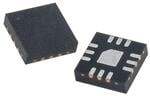
| 描述 | IC MMIC PWR AMP 3X3QFN |
| 产品分类 | RF 放大器 |
| 品牌 | Hittite Microwave Corporation |
| 数据手册 | 点击此处下载产品Datasheet |
| 产品图片 | 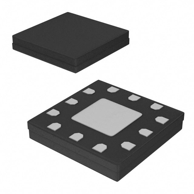 |
| P1dB | 20dBm |
| 产品型号 | HMC441LC3B |
| RF类型 | 通用 |
| rohs | 无铅 / 符合限制有害物质指令(RoHS)规范要求 |
| 产品系列 | - |
| 供应商器件封装 | 12-QFN(3x3) |
| 其它名称 | 1127-1042-6 |
| 包装 | Digi-Reel® |
| 噪声系数 | 4.5dB |
| 增益 | 14dB |
| 封装/外壳 | 12-VFQFN 裸露焊盘 |
| 标准包装 | 1 |
| 测试频率 | - |
| 电压-电源 | 5V |
| 电流-电源 | 115mA |
| 频率 | 6GHz ~ 18GHz |
Datasheet
PDF Datasheet 数据手册内容提取
HMC441LC3B v08.1017 GaAs pHEMT MMIC MEDIUM POWER AMPLIFIER, 6 - 18 GHz Typical Applications Features The HMC441LC3B is ideal for use as a medium power Gain: 14 dB T amplifier for: Saturated Output Power: +21.5 dBm @ 27% PAE M • Point-to-Point Radios Single Positive Supply: +5V @ 90 mA S • Point-to-Multi-Point Radios & VSAT 50 Ohm Matched Input/Output - R • LO Driver for HMC Mixers 12 Lead Ceramic 3x3mm SMT Package: 9mm2 E • Military EW & ECM W O P Functional Diagram General Description & The HMC441LC3B is an efficient GaAs PHEMT R MMIC Medium Power Amplifier housed in a leadless A RoHS compliant SMT package. Operating between E 6 and 18 GHz, the amplifier provides 14 dB of gain, N +21.5 dBm of saturated power and 27% PAE from LI a +5V supply. This 50 Ohm matched amplifier does not require any external components and operates - S from a single positive supply, making it an ideal R linear gain block or driver for HMC SMT mixers. The E HMC441LC3B is compatible with high volume surface I mount manufacturing techniques, and the I/Os are F I DC blocked for further ease of integration. L P M A Electrical Specifications, T = +25° C, Vdd = +5V A Parameter Min. Typ. Max. Min. Typ. Max. Min. Typ. Max. Min. Typ. Max. Units Frequency Range 6.0 - 8.5 8.5 - 12.5 12.5 - 14.0 14.0 - 18.0 GHz Gain 10 14 19 13 17 21 13 17 21 10 14 19 dB Gain Variation Over Temperature 0.015 0.02 0.015 0.02 0.015 0.02 0.015 0.02 dB/ °C Input Return Loss 10 13 20 13 dB Output Return Loss 12 15 17 14 dB Output Power for 1 dB 16 19 17 20 17 20 17 20 dBm Compression (P1dB) Saturated Output Power (Psat) 20 21.5 22.5 21.5 dBm Output Third Order Intercept (IP3) 28 30 29 32 29 32 29 32 dBm Noise Figure 4.5 6 4.5 6 4.5 6 4.5 6 dB Supply Current (Idd) 90 115 90 115 90 115 90 115 mA Information furnished by Analog Devices is believed to be accurate and reliable. However, no For price, delivery, and to place orders: Analog Devices, Inc., responsibility is assumed by Analog Devices for its use, nor for any infringements of patents or other One Technology Way, P.O. Box 9106, Norwood, MA 02062-9106 1 rliicgehntss eo fi sth girrda nptaerdti ebsy t himatp mlicaayt iroens uolrt fortohme riwtsi sues eu.n Sdpeer caifinyc aptiaotnesn ts ourb jpeactte tnot crhigahntgs eo wf Aitnhaoluotg n oDteicveic. eNso. Phone: 781-329-4700 • Order online at www.analog.com Trademarks and registered trademarks are the property of their respective owners. Application Support: Phone: 1-800-ANALOG-D
HMC441LC3B v08.1017 GaAs pHEMT MMIC MEDIUM POWER AMPLIFIER, 6 - 18 GHz Broadband Gain & Return Loss Gain vs. Temperature 20 20 15 18 T 10 16 M dB) 5 14 SPONSE ( -50 GAIN (dB) 11802 - S RE-10 6 R -15 4 E -20 2 W -25 0 O 4 6 8 10 12 14 16 18 20 6 7 8 9 10 11 12 13 14 15 16 17 18 FREQUENCY (GHz) FREQUENCY (GHz) P S21 S11 S22 +25 C +85 C -40 C & R A Input Return Loss vs. Temperature Output Return Loss vs. Temperature E N 0 0 -2 I L -5 -4 SS (dB)-10 SS (dB) --86 S - O O N L N L -10 R UR-15 UR -12 E RET RET -14 I F -20 -16 I -18 L -25 -20 P 6 7 8 9 10 11 12 13 14 15 16 17 18 6 7 8 9 10 11 12 13 14 15 16 17 18 M FREQUENCY (GHz) FREQUENCY (GHz) A +25 C +85 C -40 C +25 C +85 C -40 C P1dB vs. Temperature Psat vs. Temperature 25 25 24 24 23 23 22 22 P1dB (dBm) 122901 Psat (dBm) 122901 18 18 17 17 16 16 15 15 6 7 8 9 10 11 12 13 14 15 16 17 18 6 7 8 9 10 11 12 13 14 15 16 17 18 FREQUENCY (GHz) FREQUENCY (GHz) +25 C +85 C -40 C +25 C +85 C -40 C For price, delivery, and to place orders: Analog Devices, Inc., One Technology Way, P.O. Box 9106, Norwood, MA 02062-9106 Phone: 781-329-4700 • Order online at www.analog.com 2 Application Support: Phone: 1-800-ANALOG-D
HMC441LC3B v08.1017 GaAs pHEMT MMIC MEDIUM POWER AMPLIFIER, 6 - 18 GHz Power Compression @ 11 GHz Power Compression @ 15 GHz 30 30 SMT N (dB), PAE (%) 2205 N (dB), PAE (%) 2205 - GAI 15 GAI 15 WER Pout (dBm), 150 Pout (dBm), 150 0 0 O -10 -8 -6 -4 -2 0 2 4 6 8 10 -10 -8 -6 -4 -2 0 2 4 6 8 10 P INPUT POWER (dBm) INPUT POWER (dBm) & Pout Gain PAE Pout Gain PAE R A E Output IP3 vs. Temperature Noise Figure vs. Temperature N 36 10 LI 34 9 S - m) 3302 RE (dB) 678 B U R 3 (d 28 FIG 5 E IP 26 SE 4 FI 24 NOI 3 2 LI 22 1 P 20 0 6 7 8 9 10 11 12 13 14 15 16 17 18 6 7 8 9 10 11 12 13 14 15 16 17 18 M FREQUENCY (GHz) FREQUENCY (GHz) A +25 C +85 C -40 C +25 C +85 C -40 C Gain, Power & Output IP3 vs. Supply Voltage @ 11 GHz Reverse Isolation vs. Temperature m) 34 0 B d 32 3 ( -10 P 30 B (dBm), Psat (dBm), I 2222202468 ISOLATION (dBm)---432000 P1d 18 -50 B), 16 N (d 14 -60 AI 4.5 5 5.5 6 7 8 9 10 11 12 13 14 15 16 17 18 G Vdd (V) FREQUENCY (GHz) Gain Psat +25 C +85 C -40 C P1dB IP3 For price, delivery, and to place orders: Analog Devices, Inc., One Technology Way, P.O. Box 9106, Norwood, MA 02062-9106 Phone: 781-329-4700 • Order online at www.analog.com 3 Application Support: Phone: 1-800-ANALOG-D
HMC441LC3B v08.1017 GaAs pHEMT MMIC MEDIUM POWER AMPLIFIER, 6 - 18 GHz Additive Phase Noise Vs Offset Frequency, RF Frequency = 8 GHz, RF Input Power = 5 dBm (P1dB) T M -70 S -80 - z) -90 R H Bc/-100 E E (d-110 W OIS-120 N O E -130 S A-140 P H P-150 & -160 R -170 10 100 1K 10K 100K 1M A OFFSET FREQUENCY (Hz) E N I L Notes: - S R E I F I L P M A For price, delivery, and to place orders: Analog Devices, Inc., One Technology Way, P.O. Box 9106, Norwood, MA 02062-9106 Phone: 781-329-4700 • Order online at www.analog.com 4 Application Support: Phone: 1-800-ANALOG-D
HMC441LC3B v08.1017 GaAs pHEMT MMIC MEDIUM POWER AMPLIFIER, 6 - 18 GHz Absolute Maximum Ratings Typical Supply Current vs. Vdd Drain Bias Voltage (Vdd) +6 Vdc Vdd (V) Idd (mA) T RF Input Power (RFIN)(Vdd = +5 Vdc) +15 dBm +5.5 92 M Channel Temperature 175 °C +5.0 90 S Continuous Pdiss (T = 85 °C) +4.5 88 0.74 W (derate 8.2 mW/°C above 85 °C) - Note: Amplifier will operate over full voltage range shown above Thermal Resistance R 122 °C/W (channel to ground paddle) E Storage Temperature -65 to +150 °C W Operating Temperature -40 to +85 °C ELECTROSTATIC SENSITIVE DEVICE O ESD Sensitivity (HBM) Class 0, Passed 100V OBSERVE HANDLING PRECAUTIONS P 12-Terminal Ceramic Leadless Chip Carrier [LCC] & (E-12-4) Dimensions shown in millimeters. R Outline Drawing A E 3.05 0.36 N 2.90 SQ 0.30 I PIN 1 2.75 0.08 0.24 L INDICATOR BSC 10 12 PIN 1 - S 0.50 9 1 1.60 R BSC EXPOSED 1.50 SQ PAD E 7 3 1.40 I F 6 4 LI TOP VIEW B0.S3C2 BOTTOM VIEW P 0.90 1.00 REF M 0.80 SIDE VIEW 2.10 BSC 0.70 FOR PROPER CONNECTION OF A THE EXPOSED PAD, REFER TO SEATING THE PIN CONFIGURATION AND PKG-004837 PLANE FSUENCCTITOIONN O DF ETSHCISR IDPATTIOAN SSH EET. 03-02-2017-A 12-Terminal Ceramic Leadless Chip Carrier [LCC] (E-12-4) Dimensions shown in millimeters Package Information Part Number Package Body Material Lead Finish MSL Rating Package Marking [2] HMC441LC3B Alumina, White Gold over Nickel MSL3 [1] H441 XXXX [1] Max peak reflow temperature of 260 °C [2] 4-Digit lot number XXXX For price, delivery, and to place orders: Analog Devices, Inc., One Technology Way, P.O. Box 9106, Norwood, MA 02062-9106 Phone: 781-329-4700 • Order online at www.analog.com 5 Application Support: Phone: 1-800-ANALOG-D
HMC441LC3B v08.1017 GaAs pHEMT MMIC MEDIUM POWER AMPLIFIER, 6 - 18 GHz Pin Descriptions Pin Number Function Description Interface Schematic T Package bottom must also be 1, 3, 7, 9 GND M connected to RF/DC ground S 2 RFIN This pin is AC coupled - and matched to 50 Ohms. R E 4 - 6 This pin may be connected to RF/DC ground. 10, 12 N/C Performance will not be affected. W O This pin is AC coupled 8 RFOUT and matched to 50 Ohms. P & R A Power Supply Voltage for the amplifier. 11 Vdd E External bypass capacitors are required. N I L - Application Circuit S R E Component Value I F C1 100 pF I C2 1,000 pF L P C3 2.2 µF M A For price, delivery, and to place orders: Analog Devices, Inc., One Technology Way, P.O. Box 9106, Norwood, MA 02062-9106 Phone: 781-329-4700 • Order online at www.analog.com 6 Application Support: Phone: 1-800-ANALOG-D
HMC441LC3B v08.1017 GaAs pHEMT MMIC MEDIUM POWER AMPLIFIER, 6 - 18 GHz Evaluation PCB T M S - R E W O P & R A E N I L - S R E I F I L P M A List of Materials for Evaluation PCB 109712 [1] The circuit board used in the final application Item Description should use RF circuit design techniques. Signal J1 - J2 PCB Mount SMA Connector lines should have 50 Ohm impedance while the J3 - J4 DC Pin package ground leads and exposed paddle should C1 100 pF Capacitor, 0402 Pkg. be connected directly to the ground plane similar to C2 1000 pF Capacitor, 0603 Pkg. that shown. A sufficient number of via holes should C3 2.2 µF Capacitor, Tantalum be used to connect the top and bottom ground U1 HMC441LC3B Amplifier planes. The evaluation board should be mounted PCB [2] 109710 Evaluation PCB, 10 mils to an appropriate heat sink. The evaluation circuit [1] Reference this number when ordering complete evaluation PCB board shown is available from Analog Devices [2] Circuit Board Material: Rogers 4350 upon request. For price, delivery, and to place orders: Analog Devices, Inc., One Technology Way, P.O. Box 9106, Norwood, MA 02062-9106 Phone: 781-329-4700 • Order online at www.analog.com 7 Application Support: Phone: 1-800-ANALOG-D
Mouser Electronics Authorized Distributor Click to View Pricing, Inventory, Delivery & Lifecycle Information: A nalog Devices Inc.: HMC441LC3BTR HMC441LC3B