首页 > HMC434E > 详情
 Datasheet下载
- 型号: HMC434E
- 制造商: Hittite
- 库位|库存: xxxx|xxxx
- 要求:
| 数量阶梯 | 香港交货 | 国内含税 |
| +xxxx | $xxxx | ¥xxxx |
查看当月历史价格
查看今年历史价格
产品参数
| 参数 | 数值 |
| 产品目录 | 射频/IF 和 RFID |
| 描述 | IC FREQ DIVIDER DC-8GHZ SOT26 |
| 产品分类 | RF 其它 IC 和模块 |
| 品牌 | Hittite Microwave Corporation |
| 数据手册 | 点击此处下载产品Datasheet |
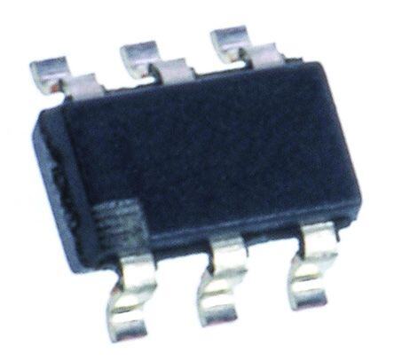
| 产品图片 |  |
| 产品型号 | HMC434E |
| RF类型 | 通用 |
| rohs | 无铅 / 符合限制有害物质指令(RoHS)规范要求 |
| 产品系列 | - |
| 供应商器件封装 | SOT-26 |
| 其它名称 | 1127-1039-2 HMC434ETR |
| 功能 | 预定标器 |
| 包装 | 带卷 (TR) |
| 封装/外壳 | SOT-23-6 |
| 标准包装 | 500 |
| 辅助属性 | 8 分型 |
| 频率 | 0Hz ~ 8GHz |
Datasheet
PDF Datasheet 数据手册内容提取
0.2 GHz to 8 GHz, GaAs, HBT MMIC, Divide by 8 Prescaler Data Sheet HMC434 FEATURES FUNCTIONAL BLOCK DIAGRAM Ultralow SSB phase noise: −150 dBc/Hz typical VCC Single-ended input/outputs HMC434 Output power: −2 dBm typical Single supply operation: 3 V Ultrasmall, surface-mount, 2.90 mm × 2.80 mm, 6-lead SOT-23 IN ÷8 OUT package ADCP tPoL CIC bAanTdIO PNLLS p rescalers GND 15684-001 Figure 1. Very small aperture terminal (VSAT) radios Unlicensed national information infrastructure (UNII) and point to point radios IEEE 802.11a and high performance radio local area network (HiperLAN) WLAN Fiber optics Cellular/3G infrastructure GENERAL DESCRIPTION The HMC434 is a low noise, static, divide by 8 prescaler The HMC434 features single-ended inputs and outputs for monolithic microwave integrated circuit (MMIC) utilizing reduced component count and cost. The low additive single indium gallium phosphide/gallium arsenide (InGaP/GaAs) sideband (SSB) phase noise of −150 dBc/Hz at 100 kHz offset heterojunction bipolar transistor (HBT) technology in an helps the user maintain optimal system noise performance. ultrasmall surface-mount 6-lead SOT-23 package. The HMC434 operates from near dc (square wave) or 200 MHz (sine wave) to 8 GHz input frequency with a single 3 V dc supply. Rev. F Document Feedback Information furnished by Analog Devices is believed to be accurate and reliable. However, no responsibility is assumed by Analog Devices for its use, nor for any infringements of patents or other One Technology Way, P.O. Box 9106, Norwood, MA 02062-9106, U.S.A. rights of third parties that may result from its use. Specifications subject to change without notice. No license is granted by implication or otherwise under any patent or patent rights of Analog Devices. Tel: 781.329.4700 ©2017 Analog Devices, Inc. All rights reserved. Trademarks and registered trademarks are the property of their respective owners. Technical Support www.analog.com
HMC434 Data Sheet TABLE OF CONTENTS Features .............................................................................................. 1 Pin Configuration and Function Descriptions ..............................5 Applications ....................................................................................... 1 Interface Schematics .....................................................................5 Functional Block Diagram .............................................................. 1 Typical Performance Characteristics ..............................................6 General Description ......................................................................... 1 Applications Information .................................................................7 Revision History ............................................................................... 2 Evaluation Board PCB ..................................................................7 Specifications ..................................................................................... 3 PCB Material Stackup ...................................................................8 Absolute Maximum Ratings ............................................................ 4 Outline Dimensions ..........................................................................9 Thermal Resistance ...................................................................... 4 Ordering Guide .............................................................................9 ESD Caution .................................................................................. 4 REVISION HISTORY 8/2017—Rev. E to Rev. F This Hittite Microwave Products data sheet has been reformatted Added Endnote 2, Table 1................................................................ 3 to meet the styles and standards of Analog Devices, Inc. 3/2017—Rev. 04.0410 to Rev. E Updated Format .................................................................. Universal Changes to Features Section, Figure 1, and General Description Section.............................................................................................................. 1 Changes to Table 1 ............................................................................. 3 Changes to Table 2 ............................................................................. 4 Added Thermal Resistance Section and Table 3; Renumbered Sequentially ........................................................................................4 Added Figure 2; Renumbered Sequentially ................................... 5 Changes to Table 4, Figure 4, Figure 5, and Figure 6 .................... 5 Changes to Figure 7, Figure 8, Figure 9, and Figure 10 ................ 6 Added Applications Information Section ...................................... 7 Changes to Evaluation Board PCB Section, Table 5, and Figure 13, and Figure 14 ................................................................... 7 Added PCB Material Stackup Section and Figure 15 ................... 8 Updated Outline Dimensions .......................................................... 9 Change to Ordering Guide ............................................................... 9 Rev. F | Page 2 of 9
Data Sheet HMC434 SPECIFICATIONS V = 3 V, T = 25°C, 50 Ω system, unless otherwise noted. P is input power. CC A IN Table 1. Parameter Min Typ Max Unit Test Conditions / Comments RADIO FREQUENCY (RF) INPUT Frequency 1, 2 0.2 8 GHz Sine wave input Power –10 0 +10 dBm f = 1.0 GHz to 3.0 GHz IN 0 0 10 dBm f = 3.0 GHz to 8.0 GHz IN RF OUTPUT SSB Phase Noise −150 dBc/Hz 100 kHz offset, P = 0 dBm, f = 4.0 GHz IN IN Power –5 –2 dBm f = 1.0 GHz to 8.0 GHz IN REVERSE LEAKAGE −25 dBm P = 0 dBm, f = 4.0 GHz, output terminated IN IN SUPPLY Voltage (V ) 2.85 3 3.15 V CC Current (I ) 62 83 mA CC 1 Below 200 MHz, a square wave input is required. 2 For stable operation without an input signal, refer to AN-1463. Rev. F | Page 3 of 9
HMC434 Data Sheet ABSOLUTE MAXIMUM RATINGS THERMAL RESISTANCE Table 2. Parameter Rating Thermal performance is directly linked to printed circuit board Supply Voltage (V ) −0.3 V to +3.5 V (PCB) design and operating environment. Careful attention to CC RF Input Power (V = 3 V) 13 dBm PCB thermal design is required. CC Temperature θ is the natural convection junction to ambient thermal JA Operating −40°C to +85°C resistance measured in a one cubic foot sealed enclosure. θ is JC Storage −65°C to +125°C the junction to case thermal resistance. Junction, T 135°C J Nominal (TA = 85°C) 99°C Table 3. Thermal Resistance Reflow 260°C Package Type θJA1 θJC2 Unit ESD Sensitivity RJ-6 359 70 °C/W Human Body Model (HBM) Class 0 1 Simulated values per JEDEC JESD51-12 standards. 2 Junction to GND package pin. Stresses at or above those listed under Absolute Maximum Ratings may cause permanent damage to the product. This is a ESD CAUTION stress rating only; functional operation of the product at these or any other conditions above those indicated in the operational section of this specification is not implied. Operation beyond the maximum operating conditions for extended periods may affect product reliability. Rev. F | Page 4 of 9
Data Sheet HMC434 PIN CONFIGURATION AND FUNCTION DESCRIPTIONS NIC 1 6 OUT HMC434 GND 2 TOP VIEW 5 VCC (Not to Scale) IN 3 4 NIC NOTES 1. NOT INTERNALLY CONNECTED. THESE PINS CAN BE CONNECTED TO RF AND DC GROUND WITHOUT ATTYHFPFEEIRCCMATALILNL YGP ETPRIEEFRDOF TROOMR AGMNNACDNE CF E(OB.R UT THE ENN HONATICN R CPEEINQDSU IARREED). 15684-002 Figure 2. Pin Configuration Table 4. Pin Function Descriptions Pin No. Mnemonic Description 1, 4 NIC Not Internally Connected. These pins can be connected to RF and dc ground without affecting performance. The NIC pins are typically tied to GND for enhanced thermal performance (but not required). 2 GND Ground. This pin must be connected to both RF and dc ground. 3 IN RF Input. This pin must be dc blocked. 5 VCC Supply Voltage (3 V). 6 OUT RF Output. This pin must be dc blocked. INTERFACE SCHEMATICS GND VCC 15684-003 50Ω OUT 15684-005 Figure 3. GND Interface Schematic Figure 5. OUT Interface Schematic VCC VCC IN 50Ω 15684-004 8pF 15684-006 Figure 4. IN Interface Schematic Figure 6. VCC Interface Schematic Rev. F | Page 5 of 9
HMC434 Data Sheet TYPICAL PERFORMANCE CHARACTERISTICS In Figure 9, P is the power of the output spectrum at the input frequency. FEEDTHROUGH 20 20 15 15 10 10 m) m) MAX PIN, TA = +85°C dB 5 dB 5 MIN PIN, TA = +85°C R ( RECOMMENDED R ( MAX PIN, TA = +25°C OWE 0 OPERATING WINDOW OWE 0 MMAINX P PININ, ,T TAA = = + –2450°°CC T P T P MIN PIN, TA = –40°C U –5 U –5 P P N N I I –10 –10 –15 –15 MAX PIN –200 1 2 3INPUT4 FREQ5UENCY6 (GHz7) 8 MIN9 PIN 10 15684-007 –200 1 2 3INPUT4 FREQ5UENCY6 (GHz7) 8 9 10 15684-010 Figure 7. Input Sensitivity Window Figure 10. Input Sensitivity Window at Various Temperatures 5 0 TA = +85°C –10 4 TTAA == –+4205°°CC –20 –30 3 Bm) 2 Bc/Hz) ––5400 R (d 1 E (d ––7600 E S UT POW –10 ASE NOI–1––098000 OUTP –2 B PH––112100 S S–130 –3 –140 –4 –150 –160 –50 1 2 3INPUT4 FREQ5UENCY6 (GHz7) 8 9 10 15684-008 –170100 1M OFFS1E0TM FREQUE1N00CMY (Hz) 1G 10G 15684-011 Figure 8. Output Power vs. Frequency at Various Temperatures Figure 11. SSB Phase Noise (PIN = 0 dBm) 0 0 –5 –5 –10 –10 –15 dBc)–20 Bm)–15 ER (–25 L (d–20 OW–30 EVE–25 P L UT –35 ER –30 P W OUT–40 PO–35 –45 –30 –50 PFEEDTHROUGH –55 SECOND HARMONIC –45 THIRD HARMONIC –600 1 2 3INPUT4 FREQ5UENCY6 (GHz7) 8 9 10 15684-009 –500 1 2 3INPUT4 FREQ5UENCY6 (GHz7) 8 9 10 15684-012 Figure 9. Output Harmonic Content (PIN = 0 dBm) Figure 12. Reverse Leakage (PIN = 0 dBm) Rev. F | Page 6 of 9
Data Sheet HMC434 APPLICATIONS INFORMATION EVALUATION BOARD PCB J3 VCC C4 Use RF circuit design techniques for the PCB used in the 10µF application. Ensure that signal lines have 50 Ω impedance when C2 the package ground leads are connected directly to the ground C3 100pF SMARFOUT plane (see Figure 14. Use a sufficient number of via holes to 1000pF J2 5 6 connect the top and bottom ground planes. VCC OUT The evaluation board has two connectors, as shown in Figure 14. U1 HMC434 The RF input connector (J1) and the RF output connector (J2) IN GND are PCB mount SMA connectors. SMA 3 2 Tcohnen eevcat ltuhaist isounp pbloya urdsi nisg pthoew Je3r e(Vd CfrCom) a nad s iJn4g (lGe N3 DV) s tuepstp plyo;i nts. RJF1IN 10C01pF GJN4D 15684-013 Figure 13. Evaluation Board Schematic See Figure 13 and Table 5 for the evaluation board schematic and the bill of materials, respectively. Table 5. List of Materials for Evaluation PCB 105675-HMC4341 Item Description J1, J2 PCB mount SMA RF connectors J3, J4 DC pins C1, C2 100 pF capacitors, 0402 package C3 1000 pF capacitors, 0402 package C4 10 μF tantalum capacitors, 1206 package U1 HMC434/HMC434E, divide by 8 PCB2 105199 evaluation board 1 105199 is the raw bare PCB identifier. Reference 105675-HMC434 when ordering the complete evaluation PCB. 2 Circuit board material: Arlon 25FR or Rogers RO4350B. 15684-014 Figure 14. Evaluation Board—Top View Rev. F | Page 7 of 9
HMC434 Data Sheet PCB MATERIAL STACKUP The evaluation board is built using Arlon 25FR or Rogers RO4350B and standard FR4 materials. RF trace widths are designed to achieve a controlled 50 Ω characteristic impedance. The complete PCB stackup is shown in Figure 15. 0.5oz (18µm) FINISHED COPPER ARLON 25FR OR ROGERS RO4350B LAMINATE 0.010" 0.5oz (18µm) FINISHED COPPER 0.0645" ± 0.0025" FR4 PREPREG COPPER TO COPPER 0.5oz (18µm) FINISHED COPPER FR4 LAMINATE 0.5oz (18µm) FINISHED COPPER 15684-015 Figure 15. Evaluation Board PCB Stackup Rev. F | Page 8 of 9
Data Sheet HMC434 OUTLINE DIMENSIONS 3.00 2.90 2.80 1.70 6 5 4 3.00 1.60 2.80 1.50 2.60 1 2 3 PIN1 INDICATOR 0.95BSC 1.90 BSC 1.30 1.15 0.90 1.45MAX 0.20MAX 0.95MIN 0.08MIN 0.55 .15MAX 10° 0.45 .05MIN 0.50MAX SPELAATNIENG 4° B0S.6C0 0.35 0.30MIN 0° COMPLIANTTOJEDECSTANDARDSMO-178-AB 12-16-2008-A Figure 16. 6-Lead Small Outline Transistor Package [SOT-23] (RJ-6) Dimensions shown in millimeters ORDERING GUIDE Model1 Temperature Range Package Description Package Option Branding HMC434 –40°C to +85°C 6-Lead Small Outline Transistor Package [SOT-23] RJ-6 H434 HMC434TR –40°C to +85°C 6-Lead Small Outline Transistor Package [SOT-23] RJ-6 H434 HMC434E –40°C to +85°C 6-Lead Small Outline Transistor Package [SOT-23] RJ-6 434E HMC434ETR –40°C to +85°C 6-Lead Small Outline Transistor Package [SOT-23] RJ-6 434E 105675-HMC434 Evaluation Board 1 The HMC434E and HMC434ETR are RoHS compliant parts. ©2017 Analog Devices, Inc. All rights reserved. Trademarks and registered trademarks are the property of their respective owners. D15684-0-8/17(F) Rev. F | Page 9 of 9