首页 > HMC427LP3E > 详情
 Datasheet下载
- 型号: HMC427LP3E
- 制造商: Hittite
- 库位|库存: xxxx|xxxx
- 要求:
| 数量阶梯 | 香港交货 | 国内含税 |
| +xxxx | $xxxx | ¥xxxx |
查看当月历史价格
查看今年历史价格
产品参数
| 参数 | 数值 |
| 产品目录 | 射频/IF 和 RFID |
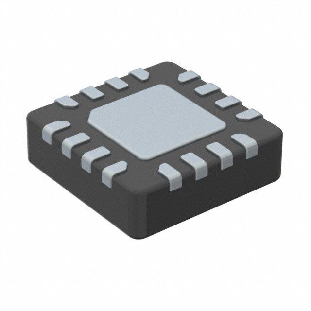
| 描述 | IC TRANSFER SWITCH 8GHZ 16-QFN |
| 产品分类 | RF 开关 |
| IIP3 | 43dBm (标准) |
| 品牌 | Hittite Microwave Corporation |
| 数据手册 | 点击此处下载产品Datasheet |
| 产品图片 |  |
| P1dB | 26dBm (标准) IP1dB |
| 产品型号 | HMC427LP3E |
| RF类型 | VSAT |
| rohs | 无铅 / 符合限制有害物质指令(RoHS)规范要求 |
| 产品系列 | - |
| 供应商器件封装 | 16-QFN(3x3) |
| 其它名称 | 1127-1383-6 |
| 包装 | Digi-Reel® |
| 封装/外壳 | 16-VFQFN 裸露焊盘 |
| 工作温度 | -40°C ~ 85°C |
| 拓扑 | 吸收性 |
| 插损@频率 | 1.2dB @ 2GHz |
| 标准包装 | 1 |
| 特性 | - |
| 电压-电源 | 5V |
| 电路 | - |
| 阻抗 | 50 欧姆 |
| 隔离@频率 | 42dB @ 2GHz(标准) |
| 频率 -上 | 8GHz |
| 频率 -下 | 0Hz |
Datasheet
PDF Datasheet 数据手册内容提取
HMC427LP3 427LP3E / v07.0805 GaAs MMIC POSITIVE CONTROL TRANSFER SWITCH, DC* - 8 GHz Typical Applications Features The HMC427LP3 / HMC427LP3E is ideal for: High Isolation: 40 ~ 45 dB thru 6 GHz • Test Instrumentation Low Insertion Loss: 1.2 dB@ 6 GHz • Fiber Optics & Broadband Telecom Non-Refl ective Design E • Basestation Infrastructure 3 x 3 mm SMT Package • Microwave Radio & VSAT T • Military Radios, Radar, & ECM Functional Diagram General Description E 10 The HMC427LP3 & HMC427LP3E are low loss broadband positive control transfer switches in leadless surface mount packages. Covering DC to 8 L GHz, this switch offers high isolation and low insertion T loss. The switch operates using a positive control M voltage of 0/+5V and requires a fi xed bias of +5V @ O S < 20 μA. - S * Blocking capacitors are required at ports RF1, 2, 3, & E 4. Their value will determine the lowest transmission fre- H S quency. C T I W B S O Electrical Specifi cations, T = +25° C, With 0/+5V Control, 50 Ohm System A Parameter Frequency Min. Typ. Max. Units DC - 6.0 GHz 1.2 1.6 dB Insertion Loss DC - 8.0 GHz 1.6 2.1 dB DC - 1.0 GHz 42 48 dB DC - 2.0 GHz 37 42 dB Isolation DC - 6.0 GHz 33 38 dB DC - 8.0 GHz 27 32 dB DC - 6.0 GHz 17 dB Return Loss DC - 8.0 GHz 15 dB Input Power for 1 dB Compression 1.0 - 8.0 GHz 23 26 dBm Input Third Order Intercept 1.0 - 8.0 GHz 37 43 dBm (Two-Tone Input Power= +7 dBm Each Tone, 1 MHz Tone Separation) Switching Characteristics DC - 8.0 GHz tRISE, tFALL (10/90% RF) 2 ns tON, tOFF (50% CTL to 10/90% RF) 4 ns Information furnisheFd obyr Apnrailocge D,e dviceesl ivis ebreylie,v eadn tod bteo a cpcularacte ea nod rrdelieabrlse., Hpowleevaers, eno coFnotra pcritc He, idtteitlieve Mry, icanrdo wtoa pvleac Ce oorrdpeorsr: aAtnioanlo:g Devices, Inc., 10 - 256 rriegshptso nosf ibthiilritdy pisa artsiessu mthea2dt m0bya yAA rnelaspluolhgt faDroe mvRi citeos sua fsoedr. i,tSs p Cuescheif,i ecnaoltrmio fnossr asfnuoyb rjiendcfrt,i nt ogM ecmhAaenn gt0se 1owf8 iptha2otue4tn tnsPo otihcr eoo.t hNneore : 9OPh7noe8n T-ee2: c57h80n1o--33lo23g9y4- 4W37 a0 y0F, a(cid:127)P .xOO:r. d 9Be7or x8o n9-l12in05e6 0,a N-t 3wor3ww7wo3o.adn, aMloAg .0c2o0m6 2-9106 lTicraednesem aisr kgsr aanndte dre gbiys teimrepdli ctraatdioenm oarr kost haerrew tihsee purnodpeerr tya noyf tphaetier nret sOopre prcadtivteeen otr w riOgnehrtnss .-olf iAnneal oag tD ewvicwesw. .hAiptptilticea.tcioonm Support: Phone: 1-800-ANALOG-D
HMC427LP3 / 427LP3E v07.0805 GaAs MMIC POSITIVE CONTROL TRANSFER SWITCH, DC* - 8 GHz Insertion Loss vs. Temperature Isolation 0 0 -10 -1 RF4 to RF1 dB) RRFF24 ttoo RRFF32 E OSS ( -2 N (dB)-20 RF1 to RF3 N L TIO-30 SERTIO -3 +25 C ISOLA-40 T N +85 C I -4 -40 C -50 -5 -60 E 0 1 2 3 4 5 6 7 8 9 0 1 2 3 4 5 6 7 8 9 FREQUENCY (GHz) FREQUENCY (GHz) 10 L Return Loss 0.1 and 1 dB Input Compression Point T 0 30 M O m) 28 ETURN LOSS (dB)---211-0505 RRRRFFFF1234 S MPRESSION POINT (dB 112222680246 CHES - S R O 1 dB Compression Point -25 T C 14 0.1 dB Compression Point T U I B NP 12 W -30 I 10 S 0 1 2 3 4 5 6 7 8 9 1 2 3 4 5 6 7 8 9 FREQUENCY (GHz) FREQUENCY (GHz) O Input Third Order Intercept Point m) 50 B d NT ( 45 OI P PT 40 E C R E 35 NT +25 C ER I 30 +-4805 CC D R O D 25 R HI T T 20 PU 1 2 3 4 5 6 7 8 9 N I FREQUENCY (GHz) Information furnisheFd obyr Apnrailocge D,e dviceesl ivis ebreylie,v eadn tod bteo a cpcularacte ea nod rrdelieabrlse., Hpowleevaers, eno coFnotra pcritc He, idtteitlieve Mry, icanrdo wtoa pvleac Ce oorrdpeorsr: aAtnioanlo:g Devices, Inc., responsibility is assume2d 0by AAnlaplohg aDe vRiceosa fodr i,ts Cushe, enolrm fosr afnoy rindfr,in gMemAen t0s 1of8 pa2te4n tsP ohr oothnere : 9O7ne8 T-e2c5h0no-3lo3gy4 W3 a yF, aP.xO:. 9B7ox8 9-120560, N-3or3w7o3od, MA 02062-9106 10 - 257 rights of third parties that may result from its use. Specifications subject to change without notice. No Phone: 781-329-4700 (cid:127) Order online at www.analog.com lTicraednesem aisr kgsr aanndte dre gbiys teimrepdli ctraatdioenm oarr kost haerrew tihsee purnodpeerr tya noyf tphaetier nret sOopre prcadtivteeen otr w riOgnehrtnss .-olf iAnneal oag tD ewvicwesw. .hAiptptilticea.tcioonm Support: Phone: 1-800-ANALOG-D
HMC427LP3 / 427LP3E v07.0805 GaAs MMIC POSITIVE CONTROL TRANSFER SWITCH, DC* - 8 GHz Absolute Maximum Ratings Bias Voltage & Current Bias Voltage Range (Vdd) +7.0 Vdc Vdd Range = +5.0 Vdc ± 10 % Control Voltage Range (A & B) -0.5V to Vdd +1.0 Vdc Vdd Idd (Typ.) Idd (Max.) Channel Temperature 150 °C (Vdc) (μA) (μA) E Thermal Resistance 130 °C/W +5.0 5 10 Storage Temperature -65 to +150 °C Control Voltages Operating Temperature -40 to +85 °C Maximum Input Power +27 dBm State Bias CondTition ESD Sensitivity (HBM) Class 1A Low 0 to +0.2 Vdc @ 5 μA Typical High Vdd ± 0.2 Vdc @ 5 μA Typical E Truth Table ELECTROSTATIC SENSITIVE DEVICE 10 OBSERVE HANDLING PRECAUTIONS Control Input Signal Path State L RF4 to RF1 to RF4 to RF2 to Note: A B RF2 RF3 RF1 RF3 DC blocking capacitors are required at ports RF1, 2, 3, & T Low High On On Off Off 4. Their value will determine the lowest transmission fre- M quency. High Low Off Off On On O S - S E H S C T I W B S O Information furnisheFd obyr Apnrailocge D,e dviceesl ivis ebreylie,v eadn tod bteo a cpcularacte ea nod rrdelieabrlse., Hpowleevaers, eno coFnotra pcritc He, idtteitlieve Mry, icanrdo wtoa pvleac Ce oorrdpeorsr: aAtnioanlo:g Devices, Inc., 10 - 258 rriegshptso nosf ibthiilritdy pisa artsiessu mthea2dt m0bya yAA rnelaspluolhgt faDroe mvRi citeos sua fsoedr. i,tSs p Cuescheif,i ecnaoltrmio fnossr asfnuoyb rjiendcfrt,i nt ogM ecmhAaenn gt0se 1owf8 iptha2otue4tn tnsPo otihcr eoo.t hNneore : 9OPh7noe8n T-ee2: c57h80n1o--33lo23g9y4- 4W37 a0 y0F, a(cid:127)P .xOO:r. d 9Be7or x8o n9-l12in05e6 0,a N-t 3wor3ww7wo3o.adn, aMloAg .0c2o0m6 2-9106 lTicraednesem aisr kgsr aanndte dre gbiys teimrepdli ctraatdioenm oarr kost haerrew tihsee purnodpeerr tya noyf tphaetier nret sOopre prcadtivteeen otr w riOgnehrtnss .-olf iAnneal oag tD ewvicwesw. .hAiptptilticea.tcioonm Support: Phone: 1-800-ANALOG-D
HMC427LP3 / 427LP3E v07.0805 GaAs MMIC POSITIVE CONTROL TRANSFER SWITCH, DC* - 8 GHz Outline Drawing E T E 10 L T NOTES: M O1. LEADFRAME MATERIAL: COPPER ALLOY S 2. DIMENSIONS ARE IN INCHES [MILLIMETERS] 3. LEAD SPACING TOLERANCE IS NON-CUMULATIVE. - 4. PAD BURR LENGTH SHALL BE 0.15mm MAXIMUM. S PAD BURR HEIGHT SHALL BE 0.05mm MAXIMUM. E 5. PACKAGE WARP SHALL NOT EXCEED 0.05mm. S 6. ALL GROUND LEADS AND GROUND PADDLE MUST BE H SOLDERED TO PCB RF GROUND. C 7. REFER TO HITTITE APPLICATION NOTE FOR SUGGESTED T LAND PATTERN. I B W Package Information S Part Number Package Body Material Lead Finish MSL Rating Package Marking [3] HMC427LP3 O Low Stress Injection Molded Plastic Sn/Pb Solder MSL1 [1] 427 XXXX HMC427LP3E RoHS-compliant Low Stress Injection Molded Plastic 100% matte Sn MSL1 [2] 427 XXXX [1] Max peak refl ow temperature of 235 °C [2] Max peak refl ow temperature of 260 °C [3] 4-Digit lot number XXXX Information furnisheFd obyr Apnrailocge D,e dviceesl ivis ebreylie,v eadn tod bteo a cpcularacte ea nod rrdelieabrlse., Hpowleevaers, eno coFnotra pcritc He, idtteitlieve Mry, icanrdo wtoa pvleac Ce oorrdpeorsr: aAtnioanlo:g Devices, Inc., responsibility is assume2d 0by AAnlaplohg aDe vRiceosa fodr i,ts Cushe, enolrm fosr afnoy rindfr,in gMemAen t0s 1of8 pa2te4n tsP ohr oothnere : 9O7ne8 T-e2c5h0no-3lo3gy4 W3 a yF, aP.xO:. 9B7ox8 9-120560, N-3or3w7o3od, MA 02062-9106 10 - 259 rights of third parties that may result from its use. Specifications subject to change without notice. No Phone: 781-329-4700 (cid:127) Order online at www.analog.com lTicraednesem aisr kgsr aanndte dre gbiys teimrepdli ctraatdioenm oarr kost haerrew tihsee purnodpeerr tya noyf tphaetier nret sOopre prcadtivteeen otr w riOgnehrtnss .-olf iAnneal oag tD ewvicwesw. .hAiptptilticea.tcioonm Support: Phone: 1-800-ANALOG-D
HMC427LP3 / 427LP3E v07.0805 GaAs MMIC POSITIVE CONTROL TRANSFER SWITCH, DC* - 8 GHz Pin Descriptions Pin Number Function Description Interface Schematic RF4, RF1, RF3, This pin is DC coupled and matched to 50 Ohm. 1, 4, 9, 12 RF2 Blocking capacitors are required. E 2, 3, 5, 8, This pin should be connected to PCB RF 10, 11, 13, N/C ground to maximize isolation. 14, 16 T Package bottom has exposed metal paddle that GND must be connected to PCB RF ground. 6 CTRLA See truth table and control voltage table. E 10 7 CTRLB See truth table and control voltage table. L 15 VDD Supply Voltage +5V ± 10%. T M O S - S E H S C T I W B S O Information furnisheFd obyr Apnrailocge D,e dviceesl ivis ebreylie,v eadn tod bteo a cpcularacte ea nod rrdelieabrlse., Hpowleevaers, eno coFnotra pcritc He, idtteitlieve Mry, icanrdo wtoa pvleac Ce oorrdpeorsr: aAtnioanlo:g Devices, Inc., 10 - 260 rriegshptso nosf ibthiilritdy pisa artsiessu mthea2dt m0bya yAA rnelaspluolhgt faDroe mvRi citeos sua fsoedr. i,tSs p Cuescheif,i ecnaoltrmio fnossr asfnuoyb rjiendcfrt,i nt ogM ecmhAaenn gt0se 1owf8 iptha2otue4tn tnsPo otihcr eoo.t hNneore : 9OPh7noe8n T-ee2: c57h80n1o--33lo23g9y4- 4W37 a0 y0F, a(cid:127)P .xOO:r. d 9Be7or x8o n9-l12in05e6 0,a N-t 3wor3ww7wo3o.adn, aMloAg .0c2o0m6 2-9106 lTicraednesem aisr kgsr aanndte dre gbiys teimrepdli ctraatdioenm oarr kost haerrew tihsee purnodpeerr tya noyf tphaetier nret sOopre prcadtivteeen otr w riOgnehrtnss .-olf iAnneal oag tD ewvicwesw. .hAiptptilticea.tcioonm Support: Phone: 1-800-ANALOG-D
HMC427LP3 / 427LP3E v07.0805 GaAs MMIC POSITIVE CONTROL TRANSFER SWITCH, DC* - 8 GHz Evaluation PCB E T E 10 L T M O S - S E S H C T I B W S O List of Materials for Evaluation PCB 105672 [1] The circuit board used in the fi nal application should Item Description be generated with proper RF circuit design tech- J1 - J4 PCB Mount SMA RF Connector niques. Signal lines at the RF port should have 50 J5 - J8 DC Pin ohm impedance and the package ground leads and C1 1000 pF Capacitor, 0603 Pkg. package bottom should be connected directly to the C2 - C5 100 pF Capacitor, 0402 Pkg. ground plane similar to that shown above. The eval- R1 - R2 100 Ohm Resistor, 0603 Pkg. uation circuit board shown above is available from HMC427LP3 / HMC427LP3E U1 Transfer Switch Hittite Microwave Corporation upon request. PCB [2] 105674 Evaluation PCB [1] Reference this number when ordering complete evaluation PCB [2] Circuit Board Material: Rogers 4350 Information furnisheFd obyr Apnrailocge D,e dviceesl ivis ebreylie,v eadn tod bteo a cpcularacte ea nod rrdelieabrlse., Hpowleevaers, eno coFnotra pcritc He, idtteitlieve Mry, icanrdo wtoa pvleac Ce oorrdpeorsr: aAtnioanlo:g Devices, Inc., responsibility is assume2d 0by AAnlaplohg aDe vRiceosa fodr i,ts Cushe, enolrm fosr afnoy rindfr,in gMemAen t0s 1of8 pa2te4n tsP ohr oothnere : 9O7ne8 T-e2c5h0no-3lo3gy4 W3 a yF, aP.xO:. 9B7ox8 9-120560, N-3or3w7o3od, MA 02062-9106 10 - 261 rights of third parties that may result from its use. Specifications subject to change without notice. No Phone: 781-329-4700 (cid:127) Order online at www.analog.com lTicraednesem aisr kgsr aanndte dre gbiys teimrepdli ctraatdioenm oarr kost haerrew tihsee purnodpeerr tya noyf tphaetier nret sOopre prcadtivteeen otr w riOgnehrtnss .-olf iAnneal oag tD ewvicwesw. .hAiptptilticea.tcioonm Support: Phone: 1-800-ANALOG-D