首页 > HMC425LP3E > 详情
 Datasheet下载
- 型号: HMC425LP3E
- 制造商: Hittite
- 库位|库存: xxxx|xxxx
- 要求:
| 数量阶梯 | 香港交货 | 国内含税 |
| +xxxx | $xxxx | ¥xxxx |
查看当月历史价格
查看今年历史价格
产品参数
| 参数 | 数值 |
| 产品目录 | 射频/IF 和 RFID |
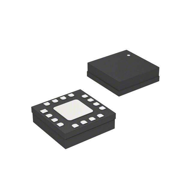
| 描述 | ATTENUATOR DGTL 6BIT 3X3QFN |
| 产品分类 | 衰减器 |
| 品牌 | Hittite Microwave Corporation |
| 数据手册 | 点击此处下载产品Datasheet |
| 产品图片 |  |
| 产品型号 | HMC425LP3E |
| rohs | 无铅 / 符合限制有害物质指令(RoHS)规范要求 |
| 产品系列 | - |
| 其它名称 | 1127-1035-2 HMC425LP3ETR |
| 功率(W) | - |
| 容差 | - |
| 封装/外壳 | 16-VFQFN 裸露焊盘 |
| 标准包装 | 500 |
| 衰减值 | 0.5dB ~ 31.5dB |
| 阻抗 | 50 欧姆 |
| 频率范围 | 2.2GHz ~ 8GHz |
Datasheet
PDF Datasheet 数据手册内容提取
HMC425LP3 425LP3E / v03.0409 0.5 dB LSB GaAs MMIC 6-BIT DIGITAL POSITIVE CONTROL ATTENUATOR, 2.2 - 8.0 GHz 5 Typical Applications Features The HMC425LP3 / HMC425LP3E is ideal for: 0.5 dB LSB Steps to 31.5 dB T M • WLAN & Point-to-Multi-Point Single Control Line Per Bit S • Fiber Optics & Broadband Telecom ± 0.5 dB Typical Bit Error - • Microwave Radio & VSAT Single +5V Supply L A • Military 3x3 mm SMT Package T I G DI Functional Diagram General Description - The HMC425LP3 & HMC425LP3E are broadband S 6-bit GaAs IC digital attenuators in low cost leadless R surface mount packages. Covering 2.2 to 8.0 GHz, O the insertion loss is less then 3.8 dB typical. The T attenuator bit values are 0.5 (LSB), 1, 2, 4, 8, and A 16 dB for a total attenuation of 31.5 dB. Attenuation U accuracy is excellent at ± 0.5 dB typical step error N with an IIP3 of +40 dBm. Six control voltage inputs, E toggled between 0 and +3 to +5V, are used to select T each attenuation state. A single Vdd bias of +3 to +5V T A is required. Electrical Specifi cations, T = +25° C, With Vdd = +5V & Vctl = 0/+5V (Unless Otherwise Noted) A Frequency Parameter Min. Typ. Max. Units (GHz) 2.2 - 6.0 GHz 3.5 3.8 dB Insertion Loss 6.0 - 8.0 GHz 3.8 4.3 dB Attenuation Range 2.2 - 8.0 GHz 31.5 dB Return Loss (RF1 & RF2, All Atten. States) 2.2 - 8.0 GHz 15 dB Attenuation Accuracy: All States 2.2 - 8.0 GHz ± 0.5 + 5% of Atten. Setting Max. dB (Referenced to Insertion Loss) Vdd = 5V 22 dBm Input Power for 0.1 dB Compression 2.2 - 8.0 GHz Vdd = 3V 19 dBm Input Third Order Intercept Point REF - 16.0 dB States 45 dBm 2.2 - 8.0 GHz (Two-Tone Input Power= 0 dBm Each Tone) 16.5 - 31.5 dB States 35 dBm Switching Characteristics 2.2 - 8.0 GHz tRISE, tFALL (10/90% RF) 160 ns tON, tOFF (50% CTL to 10/90% RF) 180 ns Information furnisheFd obry Apnrailcoge D, edviceelsi vise breylie,v eadn tdo bteo a cpcluaractee a nod rrdelieabrlse., Hpowleevaers, eno coFnotra pcritc eH, idtteiltieve rMy, iacnrdo wtoa pvlaec eC oorrdperosr: aAtnioalnog: Devices, Inc., responsibility is assumed by Analog Devices for its use, nor for any infringements of patents or other One Technology Way, P.O. Box 9106, Norwood, MA 02062-9106 5 - 116 rliicgehntss eo fi sth girrda nptaerdti ebsy t hima2tp 0mlica ayAt iorelnps uohlrt ofartoh meRr witosis uaes deu.n ,dS epCre cahinfieyc apltmiaotnessn tfs oourb rjpedactt,e tnoMt crhiAgahn tgs0 eo1 wf 8Aithn2oau4lot g n PoDtiehcveoi.c eNnso.e : P9h7o8n-e2: 75801--332394-437 0 0F (cid:127)a Ox:r d9e7r o8n-l2in5e 0at- w33w7w3.analog.com Trademarks and registered trademarks are the property of their resOpercdtivee orw Onerns.-line at www.hAiptptilticea.tcioonm Support: Phone: 1-800-ANALOG-D
HMC425* PRODUCT PAGE QUICK LINKS Last Content Update: 02/23/2017 COMPARABLE PARTS DESIGN RESOURCES View a parametric search of comparable parts. • HMC425 Material Declaration • PCN-PDN Information EVALUATION KITS • Quality And Reliability • HMC425LP3 Evaluation Board. • Symbols and Footprints DOCUMENTATION DISCUSSIONS Data Sheet View all HMC425 EngineerZone Discussions. • HMC425 Die Datasheet • HMC425LP3 Datasheet SAMPLE AND BUY Visit the product page to see pricing options. TOOLS AND SIMULATIONS • HMC425_Die S-Parameter TECHNICAL SUPPORT • HMC425LP3 S-Parameter Submit a technical question or find your regional support number. REFERENCE MATERIALS DOCUMENT FEEDBACK Quality Documentation Submit feedback for this data sheet. • Package/Assembly Qualification Test Report: 16L 3x3mm QFN Package (QTR: 11003 REV: 02) • Package/Assembly Qualification Test Report: LP2, LP2C, LP3, LP3B, LP3C, LP3D, LP3F, LP3G (QTR: 2014-0364) • Package/Assembly Qualification Test Report: Plastic Encapsulated QFN (QTR: 05006 REV: 02) • Semiconductor Qualification Test Report: MESFET-F (QTR: 2013-00247) This page is dynamically generated by Analog Devices, Inc., and inserted into this data sheet. A dynamic change to the content on this page will not trigger a change to either the revision number or the content of the product data sheet. This dynamic page may be frequently modified.
HMC425LP3 / 425LP3E v03.0409 0.5 dB LSB GaAs MMIC 6-BIT DIGITAL POSITIVE CONTROL ATTENUATOR, 2.2 - 8.0 GHz 5 Return Loss RF1, RF2 Insertion Loss (Only Major States are Shown) 0 0 T 0.5 dB 8 dB M -2 -5 1 dB 16 dB OSS (dB) -4 SS (dB)-10 24 ddBB 31.5 dB - S L O ON +25 C N L L ERTI -6 +-4805 CC ETUR-15 TA S R IN -8 -20 GI I -10 -25 D 1 2 3 4 5 6 7 8 9 10 1 2 3 4 5 6 7 8 9 10 - FREQUENCY (GHz) FREQUENCY (GHz) S R Normalized Attenuation O (Only Major States are Shown) Bit Error vs. Attenuation State T A 0 2 U dB) -5 N ATION (-10 B) 1 TE U d TEN-15 OR ( 0 T T R A A-20 R D 0.5 dB 8 dB E E 1 dB 16 dB T ALIZ-25 24 ddBB 31.5 dB BI -1 2.4 GHz M 3.5 GHz R-30 5.5 GHz O 8.0 GHz N -35 -2 1 2 3 4 5 6 7 8 9 10 0 4 8 12 16 20 24 28 32 FREQUENCY (GHz) ATTENUATION STATE (dB) Bit Error vs. Frequency Relative Phase vs. Frequency (Only Major States are Shown) (Only Major States are Shown) 2 80 1.5 0.5 dB 60 1 dB R (dB) 0.51 ASE (deg) 40 311.56248 dddddBBBBB RO 0 PH 20 R E BIT E-0.5 ATIV 0 -1 0.5 dB 8 dB EL 1 dB 16 dB R 2 dB 31.5 dB -20 -1.5 4 dB -2 -40 1 2 3 4 5 6 7 8 9 10 1 2 3 4 5 6 7 8 9 10 FREQUENCY (GHz) FREQUENCY (GHz) Information furnisheFd obry Apnrailcoge D, edviceelsi vise breylie,v eadn tdo bteo a cpcluaractee a nod rrdelieabrlse., Hpowleevaers, eno coFnotra pcritc eH, idtteiltieve rMy, iacnrdo wtoa pvlaec eC oorrdperosr: aAtnioalnog: Devices, Inc., responsibility is assumed by Analog Devices for its use, nor for any infringements of patents or other One Technology Way, P.O. Box 9106, Norwood, MA 02062-9106 rights of third parties tha2t 0ma yA relpsuhlt faro mR itos uasde. ,S pCechifiecaltmionss fsoubrjedct, toM chAan g0e1 w8ith2ou4t nPotihceo. Nnoe : P9h7o8n-e2: 75801--332394-437 0 0F (cid:127)a Ox:r d9e7r o8n-l2in5e 0at- w33w7w3.analog.com 5 - 117 license is granted by implication or otherwise under any patent or patent rights of Analog Devices. Trademarks and registered trademarks are the property of their resOpercdtivee orw Onerns.-line at www.hAiptptilticea.tcioonm Support: Phone: 1-800-ANALOG-D
HMC425LP3 / 425LP3E v03.0409 0.5 dB LSB GaAs MMIC 6-BIT DIGITAL POSITIVE CONTROL ATTENUATOR, 2.2 - 8.0 GHz 5 Worst Case Step Error Between Successive Attenuation States Bias Voltage & Current 1.2 Vdd Range = 3.0 to +5.0 Vdc T Vdd Idd (Typ.) M 0.8 (VDC) (μA) S dB) 0.4 +3.0 10 - OR ( +5.0 30 L RR 0 E A P T STE-0.4 I Control Voltage G -0.8 I State Bias Condition D -1.2 1 2 3 4 5 6 7 8 9 10 Low 0 to 0.2V @ 10 uA Typ. - FREQUENCY (GHz) High Vdd ± 0.2V @ 5 uA Typ. S R Note: Vdd = +3V to +5V O Truth Table T A U Control Voltage Input Attenua- V1 V2 V3 V4 V5 V6 tion State N 16 dB 8 dB 4 dB 2 dB 1 dB 0.5 dB RF1 - RF2 E Reference T High High High High High High I.L. T High High High High High Low 0.5 dB A High High High High Low High 1 dB High High High Low High High 2 dB High High Low High High High 4 dB High Low High High High High 8 dB Low High High High High High 16 dB Low Low Low Low Low Low 31.5 dB Any combination of the above states will provide an attenuation approximately equal to the sum of the bits selected. Information furnisheFd obry Apnrailcoge D, edviceelsi vise breylie,v eadn tdo bteo a cpcluaractee a nod rrdelieabrlse., Hpowleevaers, eno coFnotra pcritc eH, idtteiltieve rMy, iacnrdo wtoa pvlaec eC oorrdperosr: aAtnioalnog: Devices, Inc., responsibility is assumed by Analog Devices for its use, nor for any infringements of patents or other One Technology Way, P.O. Box 9106, Norwood, MA 02062-9106 5 - 118 rliicgehntss eo fi sth girrda nptaerdti ebsy t hima2tp 0mlica ayAt iorelnps uohlrt ofartoh meRr witosis uaes deu.n ,dS epCre cahinfieyc apltmiaotnessn tfs oourb rjpedactt,e tnoMt crhiAgahn tgs0 eo1 wf 8Aithn2oau4lot g n PoDtiehcveoi.c eNnso.e : P9h7o8n-e2: 75801--332394-437 0 0F (cid:127)a Ox:r d9e7r o8n-l2in5e 0at- w33w7w3.analog.com Trademarks and registered trademarks are the property of their resOpercdtivee orw Onerns.-line at www.hAiptptilticea.tcioonm Support: Phone: 1-800-ANALOG-D
HMC425LP3 / 425LP3E v03.0409 0.5 dB LSB GaAs MMIC 6-BIT DIGITAL POSITIVE CONTROL ATTENUATOR, 2.2 - 8.0 GHz 5 Absolute Maximum Ratings Control Voltage (V1 to V6) Vdd +0.5 Vdc T Bias Voltage (Vdd) +7.0 Vdc M Staorage Temperature -65 to +150 °C S Operating Temperature -40 to +85 °C - RF Input Power (2.4 - 8.0 GHz) +30 dBm L ESD Sensitivity (HBM) Class 1A A T ELECTROSTATIC SENSITIVE DEVICE I G OBSERVE HANDLING PRECAUTIONS I D - S Outline Drawing R O T A U N E T T A NOTES: 1. LEADFRAME MATERIAL: COPPER ALLOY 2. DIMENSIONS ARE IN INCHES [MILLIMETERS] 3. LEAD SPACING TOLERANCE IS NON-CUMULATIVE 4. PAD BURR LENGTH SHALL BE 0.15mm MAXIMUM. PAD BURR HEIGHT SHALL BE 0.05mm MAXIMUM. 5. PACKAGE WARP SHALL NOT EXCEED 0.05mm. 6. ALL GROUND LEADS AND GROUND PADDLE MUST BE SOLDERED TO PCB RF GROUND. 7. REFER TO HITTITE APPLICATION NOTE FOR SUGGESTED LAND PATTERN. Package Information Part Number Package Body Material Lead Finish MSL Rating Package Marking [3] HMC425LP3 Low Stress Injection Molded Plastic Sn/Pb Solder MSL1 [1] 425 XXXX HMC425LP3E RoHS-compliant Low Stress Injection Molded Plastic 100% matte Sn MSL1 [2] 425 XXXX [1] Max peak refl ow temperature of 235 °C [2] Max peak refl ow temperature of 260 °C [3] 4-Digit lot number XXXX Information furnisheFd obry Apnrailcoge D, edviceelsi vise breylie,v eadn tdo bteo a cpcluaractee a nod rrdelieabrlse., Hpowleevaers, eno coFnotra pcritc eH, idtteiltieve rMy, iacnrdo wtoa pvlaec eC oorrdperosr: aAtnioalnog: Devices, Inc., responsibility is assumed by Analog Devices for its use, nor for any infringements of patents or other One Technology Way, P.O. Box 9106, Norwood, MA 02062-9106 rights of third parties tha2t 0ma yA relpsuhlt faro mR itos uasde. ,S pCechifiecaltmionss fsoubrjedct, toM chAan g0e1 w8ith2ou4t nPotihceo. Nnoe : P9h7o8n-e2: 75801--332394-437 0 0F (cid:127)a Ox:r d9e7r o8n-l2in5e 0at- w33w7w3.analog.com 5 - 119 license is granted by implication or otherwise under any patent or patent rights of Analog Devices. Trademarks and registered trademarks are the property of their resOpercdtivee orw Onerns.-line at www.hAiptptilticea.tcioonm Support: Phone: 1-800-ANALOG-D
HMC425LP3 / 425LP3E v03.0409 0.5 dB LSB GaAs MMIC 6-BIT DIGITAL POSITIVE CONTROL ATTENUATOR, 2.2 - 8.0 GHz 5 Pin Descriptions Pin Number Function Description Interface Schematic T M Package bottom has an exposed metal paddle 1, 3, 10, 12 GND that must also be connected to RF ground. S This pin is DC coupled and matched to 50 Ohm. - 2, 11 RFIN, RFOUT Blocking capacitors are required. L A T I G 4, 5, 6, 7, 8, 9 V1 - V6 See truth table and control voltage table. I D - S R 13, 14, 16 N/C This pin should be connected to PCB RF ground to maximize performance. O T 15 Vdd Supply Voltage. A U N E T T A Information furnisheFd obry Apnrailcoge D, edviceelsi vise breylie,v eadn tdo bteo a cpcluaractee a nod rrdelieabrlse., Hpowleevaers, eno coFnotra pcritc eH, idtteiltieve rMy, iacnrdo wtoa pvlaec eC oorrdperosr: aAtnioalnog: Devices, Inc., responsibility is assumed by Analog Devices for its use, nor for any infringements of patents or other One Technology Way, P.O. Box 9106, Norwood, MA 02062-9106 5 - 120 rliicgehntss eo fi sth girrda nptaerdti ebsy t hima2tp 0mlica ayAt iorelnps uohlrt ofartoh meRr witosis uaes deu.n ,dS epCre cahinfieyc apltmiaotnessn tfs oourb rjpedactt,e tnoMt crhiAgahn tgs0 eo1 wf 8Aithn2oau4lot g n PoDtiehcveoi.c eNnso.e : P9h7o8n-e2: 75801--332394-437 0 0F (cid:127)a Ox:r d9e7r o8n-l2in5e 0at- w33w7w3.analog.com Trademarks and registered trademarks are the property of their resOpercdtivee orw Onerns.-line at www.hAiptptilticea.tcioonm Support: Phone: 1-800-ANALOG-D
HMC425LP3 / 425LP3E v03.0409 0.5 dB LSB GaAs MMIC 6-BIT DIGITAL POSITIVE CONTROL ATTENUATOR, 2.2 - 8.0 GHz 5 Evaluation PCB T M S - L A T I G I D - S R O T A U * R1 - R6 = 100 Ohm. N These resistors are optional E and may be used to enhance T decoupling of the RF path T from the control inputs. A List of Materials for Evaluation PCB 105408 [1] The circuit board used in the fi nal application should Item Description use RF circuit design techniques. Signal lines J1 - J2 PCB Mount SMA Connector should have 50 ohm impedance while the package J3 8 Pin DC Connector ground leads and exposed paddle should be con- C1 0.01 μF Capacitor, 0603 Pkg. nected directly to the ground plane similar to that C2, C3 100 pF Capacitor, 0402 Pkg. shown. A sufficient number of via holes should be R1 - R6 100 Ohm Resistor, 0603 Pkg. used to connect the top and bottom ground planes. U1 HMC425LP3 / HMC425LP3E Digital Attenuator The evaluation circuit board shown is available from PCB [2] 105260 Evaluation PCB Hittite upon request. [1] Reference this number when ordering complete evaluation PCB [2] Circuit Board Material: Rogers 4350 Information furnisheFd obry Apnrailcoge D, edviceelsi vise breylie,v eadn tdo bteo a cpcluaractee a nod rrdelieabrlse., Hpowleevaers, eno coFnotra pcritc eH, idtteiltieve rMy, iacnrdo wtoa pvlaec eC oorrdperosr: aAtnioalnog: Devices, Inc., responsibility is assumed by Analog Devices for its use, nor for any infringements of patents or other One Technology Way, P.O. Box 9106, Norwood, MA 02062-9106 rights of third parties tha2t 0ma yA relpsuhlt faro mR itos uasde. ,S pCechifiecaltmionss fsoubrjedct, toM chAan g0e1 w8ith2ou4t nPotihceo. Nnoe : P9h7o8n-e2: 75801--332394-437 0 0F (cid:127)a Ox:r d9e7r o8n-l2in5e 0at- w33w7w3.analog.com 5 - 121 license is granted by implication or otherwise under any patent or patent rights of Analog Devices. Trademarks and registered trademarks are the property of their resOpercdtivee orw Onerns.-line at www.hAiptptilticea.tcioonm Support: Phone: 1-800-ANALOG-D